

Page 1
2961
HIGH-CURRENT
HALF-BRIDGE
PRINTHEAD/MOTOR DRIVER
PRINTHEAD/MOTOR DRIVER—WITH INTERNAL
CURRENT SENSING AND CONTROL
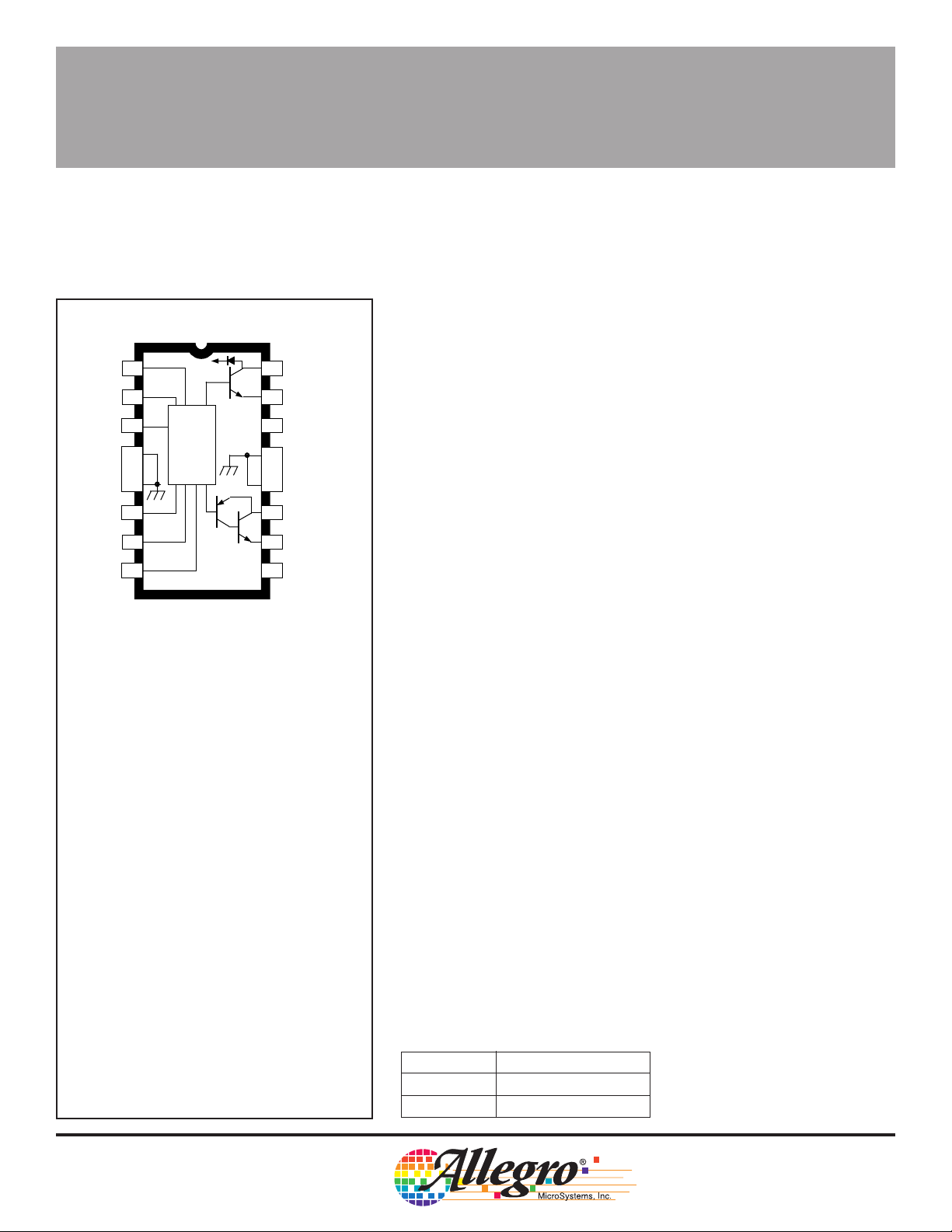
UDN2961B
V
1
REF
IN
2
3
INPUT
ENABLE
RC
MODE
4
5
6
7
8
GROUND
GROUND
ABSOLUTE MAXIMUM RATINGS
Supply Voltage, VBB. . . . . . . . . . . . . . 45 V
Output Current, I
(t
≤ 20 µs, 10% duty cycle) . . ±4.0 A
w
Logic Supply Voltage, V
Input Voltage Range,
V
. . . . . . . . . . . . . . . -0.3 V to +7.0 V
IN
Package Power Dissipation,
P
. . . . . . . . . . . . . . . . . . . See Graph
D
Operating Temperature Range,
T
. . . . . . . . . . . . . . . . -20°C to +85°C
A
Junction Temperature, T
Storage Temperature Range,
T
. . . . . . . . . . . . . . . -55°C to +150°C
S
Output current rating may be restricted to a value
determined by system concerns and factors.
These include: system duty cycle and timing,
ambient temperature, and use of any heatsinking
and/or forced cooling. For reliable operation, the
specified maximum junction temperature should
not be exceeded.
* Fault conditions that produce excessive junction
temperature will activate device thermal shutdown
circuitry. These conditions can be tolerated, but
should be avoided.
V
BB
CURRENTCONTROL
LOGIC
(continuous) . ±3.4 A
OUT
16
15
14
13
12
V
BB
11
10
9
V
CC
. . . . . . . . . 7.0 V
CC
. . . . . . . +150°C*
J
SINK OUT
EMITTER
NC
GROUND
GROUND
LOAD SUPPLY
SOURCE OUT
LOGIC SUPPLY
Dwg. PP-035
2961
HIGH-CURRENT HALF-BRIDGE
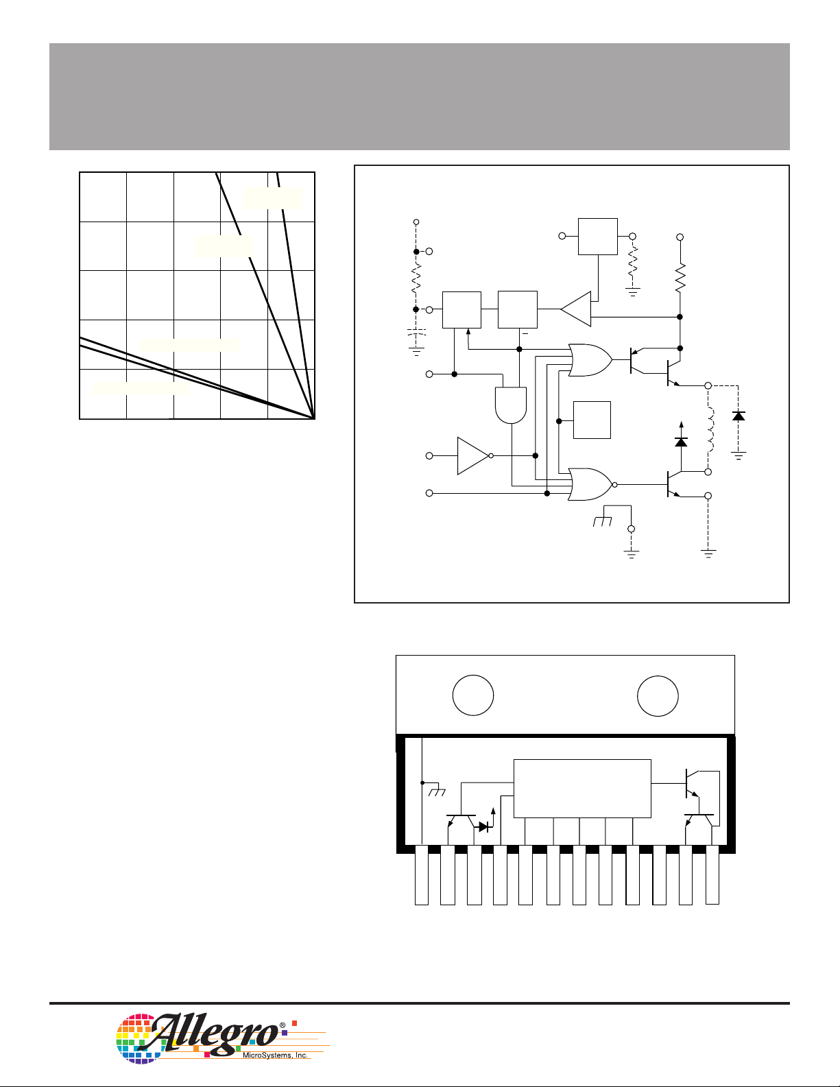
The UDN2961B and UDN2961W are 3.4 A half bridges designed
specifically for driving solenoid printheads, stepper motors, and dc
motors. The UDN2961B/W consists of a power source driver output,
a power sink driver output, a flyback recovery diode, internal current
sensing circuitry, and a user-selectable fixed off-time chopper circuit.
The output drivers are capable of sustaining 45 V with continuous
currents of ±3.4 A and peak transient currents of ±4 A permitted. The
outputs have been optimized for a low output saturation voltage
(typically 2.6 V total source plus sink drops at 3.4 A).
For output current control, load current is sensed internally and
limited by chopping the output driver(s) in a user-selectable fixed offtime PWM mode. The maximum output current is determined by the
user’s selection of a reference voltage. The MODE pin determines
whether the current control circuitry will chop in a slow current-decay
mode (only the source driver switching) or in a fast current-decay
mode (source and sink switching). A user-selectable blanking window
prevents false triggering of the current control circuitry during
chopping.
The UDN2961B is supplied in a 16-pin dual in-line plastic batwing
package with a copper lead-frame and heat sinkable tabs for improved
power dissipation capabilities. For higher power dissipation requirements, the UDN2961W is supplied in a 12-pin single in-line power tab
package.
FEATURES
■ 3.4 A, 45 V Source and Sink Drivers
■ Internal Current Sensing
■ User-Selectable Fixed Off-Time PWM Current Control
■ Internal Flyback Diode
■ Low Output Saturation Voltage
■ Chip Enable
■ Fast or Slow Current-Decay Modes
■ Programmable Blanking Window
■ Internal Thermal Shutdown Circuitry
Always order by complete part number:
Part Number Package
UDN2961B 16-Pin DIP
UDN2961W 12-Pin Power-Tab SIP
Data Sheet
29318.16*
Page 2
2961
HIGH-CURRENT
HALF-BRIDGE
PRINTHEAD/MOTOR DRIVER
10
SUFFIX 'W',
R = 2.0°C/W
θJT
8
SUFFIX 'B',
R = 6.0°C/W
θJT
6
4
SUFFIX 'W', R = 38°C/W
2
SUFFIX 'B', R = 43°C/W
0
ALLOWABLE PACKAGE POWER DISSIPATION IN WATTS
25
θJA
50 75 100 125 150
θJA
TEMPERATURE IN °C
Dwg. GP-032A
R
C
MODE
ENABLE
INPUT
FUNCTIONAL BLOCK DIAGRAM
+5 V
RC
V
LOW
TRIP
CC
ONE
SHOT
FLIPFLOP
V
REF
Q
CIRCUIT
RS
+
-
TSD
REF
V
R
CV
SENSE
2940 Ω
V
BB
SOURCE OUT
V
BB
SINK OUT
EMITTER
GROUND
UDN2961W
V
CURRENT-
V
BB
1 2 3 4 5 6 7 8 9 10 11 12
REF
V
EMITTER
GROUND
SINK OUT
CONTROL
LOGIC
V
CC
CV
R
INPUT
ENABLE
RC
MODE
SOURCE OUT
LOGIC SUPPLY
Dwg. PP-036
Dwg. FP-019A
BB
LOAD SUPPLY
115 Northeast Cutoff, Box 15036
W
Worcester, Massachusetts 01615-0036 (508) 853-5000
Copyright © 1995, 1996 Allegro MicroSystems, Inc.
Page 3

2961
HIGH-CURRENT
HALF-BRIDGE
PRINTHEAD/MOTOR DRIVER
ELECTRICAL CHARACTERISTICS at T
V
= 4.75 V to 5.25 V, R
CC
= 2940 Ω (unless otherwise noted).
CV
= +25°C, V
A
= 45 V,
BB
Limits
Characteristic Symbol Test Conditions Min. Typ. Max. Units
Output Drivers
Output Leakage Current I
Output Saturation Voltage V
Output Sustaining Voltage V
CE(SAT)
CE(sus)
Recovery Diode Leakage Current I
Recovery Diode Forward Voltage V
Motor Supply Current I
BB(on)
I
BB(off)
Output Rise Time t
Output Fall Time t
CEX
R
VEN = 0.8 V, V
= 0.8 V, V
V
EN
Source Driver, I
Source Driver, I
Sink Driver, I
Sink Driver, I
I
= ±3.4 A, L = 3 mH 45 — — V
OUT
OUT
OUT
VR = 45 V — <1.0 100 µA
F
IF = 3.4 A — — 2.0 V
VEN = 2.0 V, VIN = 0.8 V, No Load — — 70 mA
VEN = 0.8 V — — 2.5 mA
r
f
Source Driver, I
Sink Driver, I
OUT
Source Driver, I
Sink Driver, I
OUT
= 0 V — <-1.0 -100 µA
SOURCE
= 45 V — <1.0 100 µA
SINK
= -3.4 A — 1.6 2.2 V
OUT
= -3.0 A — 1.5 — V
OUT
= 3.4 A — 1.0 1.4 V
= 3.0 A — 0.9 — V
= -3.4 A — — 600 ns
OUT
= 3.4 A — — 600 ns
= -3.4 A — — 600 ns
OUT
= 3.4 A — — 600 ns
Control Logic
Logic Input Voltage V
Logic Input Current I
Reference Input Current I
Transconductance I
TRIP/VREF
Logic Supply Current I
Turn On Delay t
IN(1)
V
IN(0)
IN(1)
I
IN(0)
REF
CC
pd(on)
VIN = 5.0 V — — 10 µA
VIN = 0 V — — -1.0 mA
V
= 5.0 V — — 50 µA
REF
V
= 1.0 V 0.9 1.0 1.1 A/V
REF
= 3.2 V 0.9 1.0 1.1 A/V
V
REF
VEN = 2.0 V, VIN = 0.8 V, No Load — — 160 mA
= 0.8 V — — 15 mA
V
EN
Source Driver — — 600 ns
2.0 — — V
— — 0.8 V
Sink Driver — — 600 ns
Turn Off Delay t
pd(off)
Source Driver — — 2.0 µs
Sink Driver — — 2.0 µs
Thermal Shutdown Temperature T
Negative current is defined as coming out of (sourcing) the specified device terminal.
J
— 165 — °C
Page 4
2961
HIGH-CURRENT
HALF-BRIDGE
PRINTHEAD/MOTOR DRIVER
APPLICATIONS INFORMATION
The UDN2961B/W is a high current
half-bridge designed to drive a number of
inductive loads such as printer solenoids,
stepper motors, and dc motors. Load current
is sensed internally and is controlled by
pulse-width modulating (PWM) the output
driver(s) in a fixed off-time, variablefrequency format. The peak current level is
set by the user’s selection of a reference
voltage. A slow current-decay mode
(chopping only the source driver) or a fast
current-decay mode (chopping both the
source and sink drivers) can be selected via
the MODE pin.
PWM CURRENT CONTROL
A logic low on the MODE pin sets the
current-control circuitry into the slow-decay
mode. The RS flip-flop is set initially, and
both the source driver and the sink driver are
turned ON when the INPUT pin is at a logic
low. As current in the load increases, it is
sensed by the internal sense resistor until the
sense voltage equals the trip voltage of the
comparator. At this time, the flip-flop is reset
and the source driver is turned OFF. Over the
range of V
current trip point transfer function is a direct
linear function of the reference voltage:
To ensure an accurate chop current level
(±10%), an external 2940 Ω ±1% resistor
(RCV) is used. The actual load current peak
will be slightly higher than the trip point
(especially for low-inductance loads) because
of the internal logic and switching delays
(typically 1.5 µs). After the source driver turns
OFF, the load current decays, circulating
through an external ground clamp diode, the
load, and the sink transistor. The source
driver’s OFF time (and therefore the magnitude of the current decrease) is determined
by the one-shot’s external RC timing components:
= 0.8 V to 3.4 V, the output
REF
I
= V
TRIP
t
OFF
REF
= RC
V
SENSE
BB
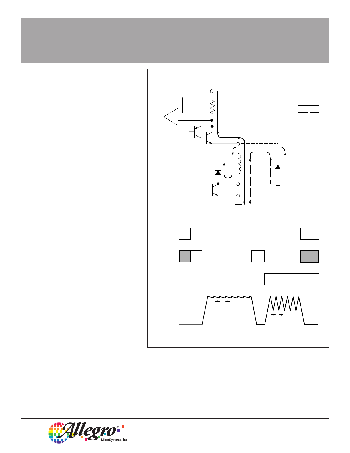
DRIVE CURRENT
RECIRCULATION (SLOW-DECAY MODE)
RECIRCULATION (FAST-DECAY MODE)
V
BB
RC
Dwg. EP-037
RC/2
Dwg. WP-015
ENABLE
INPUT
MODE
LOAD
CURRENT
REF
CIRCUIT
+
-
V
I
TRIP
within the range of 20 kΩ to 100 kΩ and 100 pF to 1000 pF. When the
one-shot times out, the flip-flop is set again, the source driver is reenabled, and the load current again is allowed to rise to the set peak
value and trip the comparator. This cycle repeats itself, maintaining the
average load current at the desired level.
115 Northeast Cutoff, Box 15036
Worcester, Massachusetts 01615-0036 (508) 853-5000
Page 5

2961
HIGH-CURRENT
HALF-BRIDGE
PRINTHEAD/MOTOR DRIVER
A logic high on the MODE pin sets the
current-control circuitry into the fast-decay
mode. When the peak current threshold is
detected, the flip-flop is reset and both the
source driver and the sink driver turn OFF.
Load current decays quickly through the
external ground clamp diode, the load, and
the internal flyback diode. In the fastdecay mode, the OFF time period is onehalf the time that is set by the external RC
network for the slow-decay mode:
t
The amount of ripple current, when
chopping in the fast-decay mode, is
considerably higher than when chopping in
the slow-decay mode.
The frequency of the PWM current
control is determined by the time required
for the load current to reach the set peak
threshold (a function of the load characteristics and VBB) plus the OFF time of the
switching driver(s) (set by the external RC
components).
To prevent false resetting of the flipflop, due to switching transients and noise,
a blanking time for the comparator can be
set by the user where tB ≈ 3600 x C in the
slow-decay mode or tB ≈ 2400 x C in the
fast-decay mode. For C between 100 pF
and 1000 pF, tB is in µs.
OFF
=
RC
2
V
REF
INPUT
ENABLE
MODE
INPUT
2940 Ω
±1%
CURRENTCONTROL
LOGIC
R
CURRENTCONTROL
LOGIC
R
V
BB
V
BB
1
2
3
4
5
6
7
8
C
1
2
3
4
±1%
2940 Ω
5
6
C
7
8
16
15
14
13
V
47 µF
+5 V
BB
47 µF
V
BB
Dwg. EP-038A
12
V
BB
11
10
9
V
CC
+5 V
16
15
14
13
12
V
BB
11
10
9
V
CC
POWER CONSIDERATIONS
The UDN2961B/W outputs are optimized for low power dissipation. The sink
driver has a maximum saturation voltage
drop of only 1.4 V at 3.4 A, while the
source driver has a 2.2 V drop at -3.4 A.
Device power dissipation is minimized in
the slow-decay mode, as the chopping
driver (the source driver) is ON for less
than 50% of the chop period. When the
source driver is OFF during a chop cycle,
power is dissipated on chip only by the sink
driver; the rest of the power is dissipated
through the external ground clamp diode.
In the fast-decay mode, the ON time of the
chopping drivers (both the source driver
and the sink driver) may be greater than 50%, and the power dissipation will be greater.
GENERAL
A logic low on the ENABLE pin prevents the source driver and the
sink driver from turning ON, regardless of the state of the INPUT pin or
the supply voltages. With the ENABLE pin high, a logic low on the
INPUT pin turns ON the output drivers.
To protect against inductive load voltage transients, an external
ground clamp diode is required. A fast-recovery diode is recommended to reduce power dissipation in the UDN2961B/W. The blanking time prevents false triggering of the current sense comparator,
which can be caused by the recovery current spike of the ground
clamp diode when the chopping source driver turns ON.
Page 6

2961
HIGH-CURRENT
HALF-BRIDGE
PRINTHEAD/MOTOR DRIVER
The load supply (VBB) should be well decoupled with a capacitor
placed as close as possible to the device.
The EMITTER pin should be connected to a high-current power
ground.
Thermal shutdown protection circuitry is activated and turns OFF
both output drivers at a junction temperature of typically +165°C. It is
intended only to protect the device from catastrophic failures due to
excessive junction temperatures and should not imply that output short
circuits are permitted. The output drivers are re-enabled when the
junction temperature cools down to approximately +145°C.
MOTOR DRIVER APPLICATIONS
Two UDN2961B/Ws can be cross connected as shown to form a
full-bridge driver circuit. Two full-bridge circuits are needed to drive a
two-phase bipolar stepper motor. When in a full-bridge configuration,
one INPUT signal must be logically inverted from the other INPUT
signal to prevent the simultaneous conduction of a source driver from
one half-bridge and the sink driver from the other half-bridge. In order
to prevent crossover currents, a turn-ON delay time of 3 µs is needed
between the time an INPUT signal for one of the half bridges goes high
and the INPUT signal for the other half bridge goes low.
In addition to the two external ground clamp diodes, diodes in
series with the load to the SINK OUT are needed in a full-bridge
configuration. These series diodes prevent the sink drivers from
conducting on the inverse mode, which can occur when the opposite
half-bridge ground clamp diode is conducting and forces the sink driver
collector below ground.
If fast current decay is used (MODE = logic high) or pulse width
modulation of the load-current direction is used, diodes in series with
the load to the SOURCE OUT are needed. These series diodes
prevent the SOURCE OUT from inverse conducting during the recirculation period and thereby prevent shoot-through currents from occuring
as the drivers turn back ON.
115 Northeast Cutoff, Box 15036
Worcester, Massachusetts 01615-0036 (508) 853-5000
Page 7

2961
HIGH-CURRENT
HALF-BRIDGE
PRINTHEAD/MOTOR DRIVER
(controlling dimensions)
16
0.280
0.240
NOTE 4
UDN2961B
Dimensions in Inches
9
0.020
0.008
0.300
BSC
0.430
MAX
0.210
MAX
7.11
6.10
0.015
MIN
1
0.070
0.045
16
1
1.77
1.15
0.022
0.014
0.100
0.775
BSC
0.735
Dimensions in Millimeters
(for reference only)
NOTE 4
2.54
19.68
18.67
BSC
8
0.005
MIN
0.150
0.115
Dwg. MA-001-17A in
0.508
9
8
0.13
MIN
0.204
7.62
BSC
10.92
MAX
5.33
MAX
0.39
MIN
0.558
0.356
NOTES: 1. Exact body and lead configuration at vendor’s option within limits shown.
2. Lead spacing tolerance is non-cumulative
3. Lead thickness is measured at seating plane or below.
4. Webbed lead frame. Leads 4, 5, 12, and 13 are internally one piece.
3.81
2.93
Dwg. MA-001-17A mm
Page 8

2961
HIGH-CURRENT
HALF-BRIDGE
PRINTHEAD/MOTOR DRIVER
(controlling dimensions)
UDN2961W
Dimensions in Inches
INDEX
AREA
0.065
0.035
0.020
1.260
1.240
0.775
0.765
0.245
0.225
0.140
0.365
1
0.030
0.020
12
0.100
±0.010
0.180
0.155
0.145
0.290
MAX
ø
0.570
0.540
MIN
0.023
0.018
0.055
0.045
0.135
0.100
0.080
0.070
Dwg. MP-007 in
NOTES: 1. Lead thickness is measured at seating plane or below.
2. Lead spacing tolerance is non-cumulative
3. Exact body and lead configuration at vendor’s option within limits shown.
4. Lead gauge plane is 0.030” below seating plane.
115 Northeast Cutoff, Box 15036
Worcester, Massachusetts 01615-0036 (508) 853-5000
Page 9

2961
HIGH-CURRENT
HALF-BRIDGE
PRINTHEAD/MOTOR DRIVER
Dimensions in Millimeters
UDN2961W
(for reference only)
INDEX
AREA
1.65
0.89
0.51
32.00
31.49
19.69
19.45
6.22
5.71
3.56
9.27
1
0.76
0.51
12
2.54
±0.254
3.94
3.68
4.57
MAX
ø
14.48
13.71
7.36
MIN
0.59
0.45
1.40
1.14
3.43
2.54
2.03
1.77
Dwg. MP-007 mm
NOTES: 1. Lead thickness is measured at seating plane or below.
2. Lead spacing tolerance is non-cumulative
3. Exact body and lead configuration at vendor’s option within limits shown.
4. Lead gauge plane is 0.762 mm below seating plane.
Page 10

2961
HIGH-CURRENT
HALF-BRIDGE
PRINTHEAD/MOTOR DRIVER
This page intentionally left blank
115 Northeast Cutoff, Box 15036
Worcester, Massachusetts 01615-0036 (508) 853-5000
Page 11

2961
HIGH-CURRENT
HALF-BRIDGE
PRINTHEAD/MOTOR DRIVER
This page intentionally left blank
Page 12

2961
HIGH-CURRENT
HALF-BRIDGE
PRINTHEAD/MOTOR DRIVER
MOTOR DRIVERS SELECTION GUIDE
Function Output Ratings * Part Number †
INTEGRATED CIRCUITS FOR BRUSHLESS DC MOTORS
3-Phase Controller/Drivers ±2.0 A 45 V 2936 and 2936-120
Hall-Effect Latched Sensors 10 mA 24 V 3175 and 3177
2-Phase Hall-Effect Sensor/Controller 20 mA 25 V 3235
Hall-Effect Complementary-Output Sensor 20 mA 25 V 3275
2-Phase Hall-Effect Sensor/Driver 900 mA 14 V 3625
2-Phase Hall-Effect Sensor/Driver 400 mA 26 V 3626
Hall-Effect Complementary-Output Sensor/Driver 300 mA 60 V 5275
3-Phase Back-EMF Controller/Driver ±900 mA 14 V 8902–A
3-Phase Controller/DMOS Driver ±4.0 A 14 V 8925
3-Phase Back-EMF Controller/Driver ±1.0 A 7 V 8984
INTEGRATED BRIDGE DRIVERS FOR DC AND BIPOLAR STEPPER MOTORS
PWM Current-Controlled Dual Full Bridge ±750 mA 45 V 2916
PWM Current-Controlled Dual Full Bridges ±1.5 A 45 V 2917 and 2918
PWM Current-Controlled Dual Full Bridge ±750 mA 45 V 2919
Dual Full-Bridge Driver ±2.0 A 50 V 2998
PWM Current-Controlled Full Bridge ±2.0 A 50 V 3952
PWM Current-Controlled Full Bridge ±1.3 A 50 V 3953
PWM Current-Controlled Microstepping Full Bridges ±1.5 A 50 V 3955 and 3957
PWM Current-Controlled Dual Full Bridge ±800 mA 33 V 3964
PWM Current-Controlled Dual Full Bridge ±650 mA 30 V 3966 and 3968
PWM Current-Controlled Dual Full Bridge ±750 mA 45 V 6219
OTHER INTEGRATED CIRCUIT & PMCM MOTOR DRIVERS
Unipolar Stepper-Motor Quad Driver 1.8 A 50 V 2544
Unipolar Stepper-Motor Translator/Driver 1.25 A 50 V 5804
Unipolar Stepper-Motor Quad Drivers 1 A 46 V 7024 and 7029
Unipolar Microstepper-Motor Quad Driver 1.2 A 46 V 7042
Voice-Coil Motor Driver ±500 mA 6 V 8932–A
Voice-Coil Motor Driver ±800 mA 16 V 8958
Voice-Coil (and Spindle) Motor Driver ±350 mA 7 V 8984
* Current is maximum specified test condition, voltage is maximum rating. See specification for sustaining voltage limits
or over-current protection voltage limits. Negative current is defined as coming out of (sourcing) the output.
† Complete part number includes additional characters to indicate operating temperature range and package style.
Allegro MicroSystems, Inc. reserves the right to make, from time to time, such departures from the
detail specifications as may be required to permit improvements in the design of its products.
The information included herein is believed to be accurate and reliable. However, Allegro
MicroSystems, Inc. assumes no responsibility for its use; nor for any infringements of patents or other
rights of third parties which may result from its use.
115 Northeast Cutoff, Box 15036
Worcester, Massachusetts 01615-0036 (508) 853-5000
 Loading...