

Page 1
REF 1
V
44
PWM 1
24
21
I
1
PHASE
43
θ
PWM 2
25
REF 2
V
ENABLE
424140
1
θ
26
PHASE
1
1
RC
1
EN
2
2
EN
27
2
2
ENABLE
1
1A
OUT
6
GND
7
8
9
10
11
12
13
14
15
16
GND
17 29
18
2A
OUT
1B
1
E
SENSE
4
5
1
2
19
20
2
2
E
SENSE
OUT
3
21
OUT
2B
11
10
I
I
2
1
BB
V
22
23
20
I
LOAD SUPPLY
ABSOLUTE MAXIMUM RATINGS
at TJ ≤ +150°C
LOGIC SUPPLY
CC
V
39
38
37
36
35
34
33
32
31
30
28
2
RC
Dwg. PP-021
Dwg. PP-021
GND
GND
29319.22†
2 9 1 7
DUAL FULL-BRIDGE
PWM MOTOR DRIVER
The UDN2917EB motor driver is designed to drive both windings
of a bipolar stepper motor or bidirectionally control two dc motors. Both
bridges are capable of sustaining 45 V and include internal pulse-width modula-
tion (PWM) control of the output current to 1.5 A.
For PWM current control, the maximum output current is determined by the
user’s selection of a reference voltage and sensing resistor. Two logic-level
inputs select output current limits of 0, 33%, 67%, or 100% of the maximum
level. A PHASE input to each bridge determines load current direction. Active-
low ENABLE inputs control the four drivers in each bridge.
The bridges include both ground clamp and flyback diodes for protection
against inductive transients. Internally generated delays prevent cross-over
currents when switching current direction. Special power-up sequencing is not
required. Thermal protection circuitry disables the outputs if the chip tempera-
ture exceeds safe operating limits.
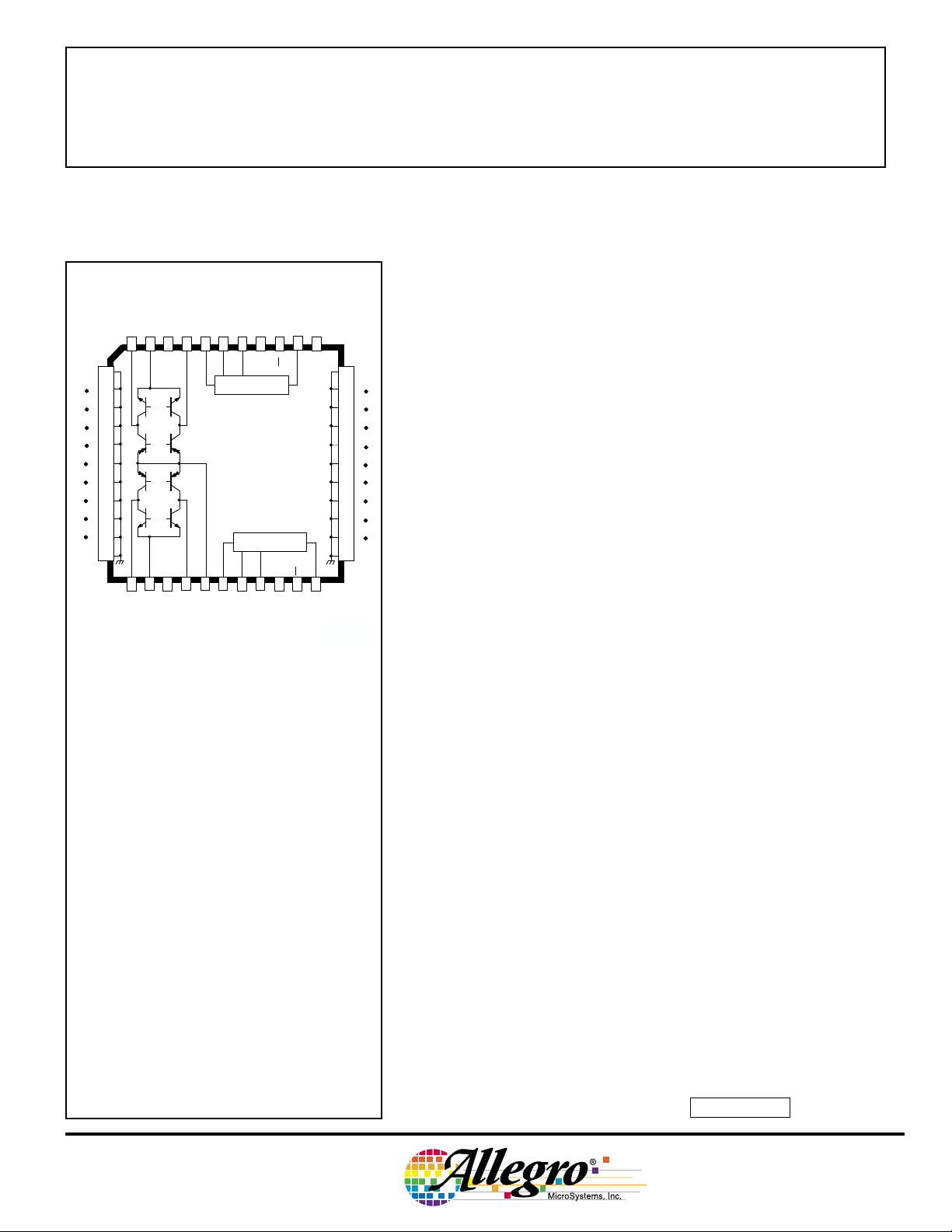
The UDN2917EB is supplied in a 44-lead power PLCC for surface-mount
applications. Its batwing construction provides for maximum package power
dissipation in the smallest possible construction. The UDN2917EB is available
for operation from -40°C to +85°C. To order, change the prefix from 'UDN' to
'UDQ'. This device is also available on special order for operation to +125°C.
Data Sheet
Motor Supply Voltage, VBB.................... 45 V
Output Current, I
(tw ≤ 20 µs) ..... ±1.75 A
OUT
(Continuous) ............................... ±1.5 A
Logic Supply Voltage, V
.................... 7.0 V
CC
Logic Input Voltage Range,
VIN................................ -0.3 V to +7.0 V
Output Emitter Voltage, V
................... 1.0 V
E
Package Power Dissipation,
PD......................................... See Graph
Operating Temperature Range,
T
.................................. -20°C to +85°C
A
Storage Temperature Range,
T
................................ -55°C to +150°C
S
Output current rating may be limited by duty cycle,
ambient temperature, and heat sinking. Under any
set of conditions, do not exceed the specified peak
current rating or a junction temperature of +150°C.
FEATURES
■ 1.5 A Continuous Output Current
■ 45 V Output Sustaining Voltage
■ Internal Clamp Diodes
■ Digital Control of Output Current
■ Internal Thermal Shutdown Circuitry
■ Similar to Dual PBL3770
Always order by complete part number: UDN2917EB .
Page 2
2917
DUAL FULL-BRIDGE
PWM MOTOR DRIVER
PWM CURRENT-CONTROL CIRCUITRY
CHANNEL 1
PIN NUMBERS
SHOWN.
V
44
REF
20 kΩ
OUT
V
BB
22
OUT
B
36
A
5
E
12.5
10
7.5
÷10
40 kΩ
10 kΩ
2
I
0
1
I
1
R
S
R
C
SENSE
–
4
+
C
C
ONE
SHOT
41
RC
R
T
SOURCE
DISABLE
C
T
Dwg. EP-007-2A
TRUTH TABLE
R
=
θJT
Enable Phase Out
6
°C
/W
LHHL
LLLH
A
HXZZ
X = Don’t care
Z = High impedance
Out
B
5.0
2.5
0
ALLOWABLE PACKAGE POWER DISSIPATION IN WATTS
25
R = 30
θ
J
A
°C/W
50 75 100 125 150
TEMPERATURE IN °C
Dwg. GP-020B
115 Northeast Cutoff, Box 15036
Worcester, Massachusetts 01615-0036 (508) 853-5000
Copyright © 1991, 2000 Allegro MicroSystems, Inc.
Page 3

2917
DUAL FULL-BRIDGE
PWM MOTOR DRIVER
ELECTRICAL CHARACTERISTICS at T
= +25°C, VBB = 45 V, VCC = 5.0 V, V
A
= 5.0 V (unless
REF
otherwise noted).
Limits
Characteristic Symbol Test Conditions Min. Typ. Max. Units
Output Drivers (OUT
Motor Supply Range V
Output Leakage Current I
Output Sustaining Voltage V
Output Saturation Voltage V
Clamp Diode Leakage Current I
Clamp Diode Forward Voltage V
Driver Supply Current I
Control Logic
or OUTB)
A
BB
CEX
CE(sus)
CE(SAT
R
F
BB(ON)
I
BB(OFF)
10 — 45 V
V
= V
OUT
BB
= 0 — <-1.0 -50 µA
V
OUT
I
= ±1.5 A, L = 3.5 mH 45 —— V
OUT
)
Sink Driver, I
Sink Driver, I
Source Driver, I
Source Driver, I
= +1.0 A* — 0.5 0.7 V
OUT
= +1.5 A* — 0.8 1.0 V
OUT
= -1.0 A* — 1.8 1.9 V
OUT
= -1.5 A* — 1.9 2.1 V
OUT
— <1.0 50 µA
VR = 45 V — <1.0 50 µA
IF = 1.5 A — 1.6 2.0 V
Both Bridges On, No Load — 9.0 12 mA
Both Bridges Off — 4.0 6.0 mA
Input Voltage V
Input Current I
Reference Voltage Range V
Current Limit Threshold V
(at trip point)
Thermal Shutdown Temp. T
Total Logic Supply Current I
IN(1)
V
IN(0)
IN(1)
I
IN(0)
REF
REF/VSENSE
J
CC(ON)
I
CC(OFF)
All Inputs 2.4 —— V
All Inputs ——0.8 V
V
= 2.4 V — <1.0 20 µA
IN
VIN = 0.8 V — -3.0 -200 µA
Operating 1.5 — 7.5 V
I0 = I1 = 0.8 V 9.5 10 10.5 —
= 2.4 V, I1= 0.8 V 13.5 15 16.5 —
I
0
= 0.8 V, I1 = 2.4 V 25.5 30 34.5 —
I
0
I0 = I1 = VEN = 0.8 V, No Load — 90 105 mA
I0 = I1 = 2.4 V, No Load — 10 12 mA
Negative current is defined as coming out of (sourcing) the specified device pin.
Typical Data is for design information only.
* Pulse test (<10 ms).
www.allegromicro.com
— 170 — °C
Page 4

2917
DUAL FULL-BRIDGE
PWM MOTOR DRIVER
APPLICATIONS INFORMATION
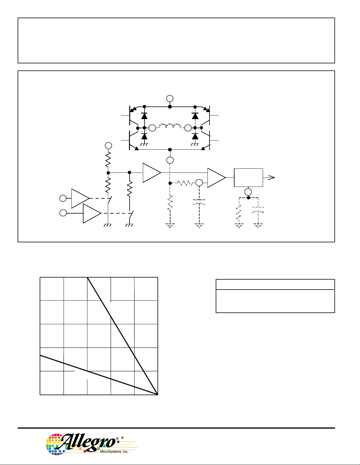
PWM CURRENT CONTROL
The UDN2917EB dual bridge is designed
to drive both windings of a bipolar stepper
motor. Output current is sensed and controlled independently in each bridge by an
external sense resistor (R
parator, and monostable multivibrator.
), internal com-
S
PWM OUTPUT CURRENT WAVEFORM
V
PHASE
When the bridge is turned on, current
increases in the motor winding and it is
sensed by the external sense resistor until the
sense voltage (V
) reaches the level set
SENSE
at the comparator’s input:
I
TRIP
= V
REF
/10 R
S
The comparator then triggers the monostable which turns off the source driver of
the bridge. The actual load current peak will
be slightly higher than the trip point (especially for low-inductance loads) because of
the internal logic and switching delays. This
delay (td) is typically 2 µs. After turn-off, the
motor current will normally decay, circulating
through the ground clamp diode and sink
transistor. The source driver’s off time (and
therefore the magnitude of the current decrease) is determined by the monostable’s
external RC timing components, where t
=
off
RTCT within the range of 20 kΩ to 100 kΩ and
200 pF to 500 pF.
When the source driver is re-enabled, the
winding current (the sense voltage) is again
allowed to rise to the comparator’s threshold.
This cycle repeats itself, maintaining the
average motor winding current at the desired
level.
+
I
0
OUT
–
I
TRIP
t
d
t
off
Dwg. WM-003-1A
LOAD CURRENT PATHS
V
BB
Special circuitry has been included to
prevent runaway current control when the
fixed off time (t
) is set too short. This
off
circuitry prevents the source driver from being
re-enabled until the load current has decayed
to below the I
TRIP
level.
R
S
BRIDGE ON
SOURCE OFF
ALL OFF
115 Northeast Cutoff, Box 15036
Worcester, Massachusetts 01615-0036 (508) 853-5000
Dwg. EP-006-1
Page 5

2917
DUAL FULL-BRIDGE
PWM MOTOR DRIVER
CURRENT-CONTROL
TRUTH TABLE
I
0
LLV
HLV
LHV
HH 0
I
1
Output Current
/10 RS = I
REF
/15 RS = 2/3 I
REF
/30 RS = 1/3 I
REF
TRIP
TRIP
TRIP
Loads with high distributed capacitances may result in high turn-on
current peaks. This peak (appearing across RS) will attempt to trip the
comparator, resulting in erroneous current control or high-frequency
oscillations. An external RCCC low-pass filter may be needed to delay
the action of the comparator.
LOGIC CONTROL OF OUTPUT CURRENT
Two logic level inputs (I0 and I1) allow digital selection of the motor
winding current at 100%, 67%, 33%, or 0% of the maximum level per
the table. The 0% output current condition turns off all drivers in the
bridge and can be used as an output enable function. These logic level
inputs greatly enhance the implementation of µP-controlled drive
formats.
During half-step operations, the I0 and I1 inputs allow the µP to
control the motor at a constant torque between all positions in an eightstep sequence. This is accomplished by digitally selecting 100% drive
current when only one phase is on and 67% drive current when two
phases are on.
The logic control inputs can also be used to select a reduced
current level (and reduced power dissipation) for ‘hold’ conditions
and/or increased current (and available torque) for start-up conditions.
GENERAL
To avoid excessive voltage spikes on the LOAD SUPPLY pin
(VBB), a large-value capacitor (≥47 µF) should be connected from V
BB
to ground as close as possible to the device. Under no circumstances
should the voltage at LOAD SUPPLY exceed 45 V.
The PHASE input to each bridge determines the direction motor
winding current flows. An internally generated deadtime (approximately 3 µs) prevents crossover currents that can occur when switching the PHASE input.
All four drivers in the bridge output can be turned off (VEN ≥ 2.4 V
or I0 = I1 ≥ 2.4 V), resulting in a fast current decay through the internal
output clamp and flyback diodes. The fast current decay is desirable
in half-step and high-speed applications. All logic inputs float high; the
ENABLE input must be tied low if it is not used.
Varying the reference voltage (V
) provides continuous control
REF
of the peak load current for micro-stepping applications, within the
specified limits for V
REF
.
Thermal protection circuitry turns off all drivers when the junction
temperature reaches +170°C. It is only intended to protect the device
from failures due to excessive junction temperature and should not
imply that output short circuits are permitted. The output drivers are
re-enabled when the junction temperature cools to +145°C.
www.allegromicro.com
Page 6

2917
DUAL FULL-BRIDGE
PWM MOTOR DRIVER
UDN2917EB
Dimensions in Inches
(controlling dimensions)
28
18
0.319
0.291
0.319
0.291
8.10
7.39
8.10
7.39
0.021
0.013
0.050
BSC
0.533
0.331
1.27
BSC
0.020
MIN
0.180
0.165
29
0.032
0.026
0.695
0.685
0.656
0.650
39
40
Dimensions in Millimeters
(for reference only)
28
29
0.812
0.661
17.65
17.40
16.662
16.510
39
0.656
0.650
144
0.695
0.685
INDEX AREA
2
INDEX AREA
17
7
6
Dwg. MA-005-44A in
18
17
7
0.51
MIN
4.57
4.20
NOTES: 1. MO-047AC except for terminal shoulder height.
2. Webbed lead frame. Leads 7-17 and 29-39 are internally one piece.
3. Lead spacing tolerance is non-cumulative.
4. Exact body and lead configuration at vendor’s option within limits shown.
5. Supplied in standard sticks/tubes of 27 devices or add “TR” to part number for tape and reel.
115 Northeast Cutoff, Box 15036
Worcester, Massachusetts 01615-0036 (508) 853-5000
144
17.65
17.40
2
6
Dwg. MA-005-44A mm
40
16.662
16.510
Page 7

2917
DUAL FULL-BRIDGE
PWM MOTOR DRIVER
www.allegromicro.com
The products described here are manufactured under one or more
U.S. patents or U.S. patents pending.
Allegro MicroSystems, Inc. reserves the right to make, from time to
time, such departures from the detail specifications as may be required
to permit improvements in the performance, reliability, or
manufacturability of its products. Before placing an order, the user is
cautioned to verify that the information being relied upon is current.
Allegro products are not authorized for use as critical components
in life-support devices or systems without express written approval.
The information included herein is believed to be accurate and
reliable. However, Allegro MicroSystems, Inc. assumes no responsibility for its use; nor for any infringement of patents or other rights of
third parties which may result from its use.
Page 8

2917
DUAL FULL-BRIDGE
PWM MOTOR DRIVER
MOTOR DRIVERS
Function Output Ratings* Part Number
INTEGRATED CIRCUITS FOR BRUSHLESS DC MOTORS
3-Phase Power MOSFET Controller — 28 V 3933
3-Phase Power MOSFET Controller — 50 V 3932
3-Phase Power MOSFET Controller — 50 V 7600
2-Phase Hall-Effect Sensor/Driver 400 mA 26 V 3626
Bidirectional 3-Phase Back-EMF Controller/Driver ±600 mA 14 V 8906
2-Phase Hall-Effect Sensor/Driver 900 mA 14 V 3625
3-Phase Back-EMF Controller/Driver ±900 mA 14 V 8902–A
3-Phase Controller/Drivers ±2.0 A 45 V 2936 & 2936-120
INTEGRATED BRIDGE DRIVERS FOR DC AND BIPOLAR STEPPER MOTORS
Dual Full Bridge with Protection & Diagnostics ±500 mA 30 V 3976
PWM Current-Controlled Dual Full Bridge ±650 mA 30 V 3966
PWM Current-Controlled Dual Full Bridge ±650 mA 30 V 3968
PWM Current-Controlled Dual Full Bridge ±750 mA 45 V 2916
PWM Current-Controlled Dual Full Bridge ±750 mA 45 V 2919
PWM Current-Controlled Dual Full Bridge ±750 mA 45 V 6219
PWM Current-Controlled Dual Full Bridge ±800 mA 33 V 3964
PWM Current-Controlled Full Bridge ±1.3 A 50 V 3953
PWM Current-Controlled Dual Full Bridge ±1.5 A 45 V 2917
PWM Current-Controlled Microstepping Full Bridge ±1.5 A 50 V 3955
PWM Current-Controlled Microstepping Full Bridge ±1.5 A 50 V 3957
PWM Current-Controlled Dual DMOS Full Bridge ±1.5 A 50 V 3972
Dual Full-Bridge Driver ±2.0 A 50 V 2998
PWM Current-Controlled Full Bridge ±2.0 A 50 V 3952
DMOS Full Bridge PWM Driver ±2.0 A 50 V 3958
Dual DMOS Full Bridge ±2.5 A 50 V 3971
UNIPOLAR STEPPER MOTOR & OTHER DRIVERS
Voice-Coil Motor Driver ±500 mA 6 V 8932–A
Voice-Coil Motor Driver ±800 mA 16 V 8958
Unipolar Stepper-Motor Quad Drivers 1 A 46 V 7024 & 7029
Unipolar Microstepper-Motor Quad Driver 1.2 A 46 V 7042
Unipolar Stepper-Motor Translator/Driver 1.25 A 50 V 5804
Unipolar Stepper-Motor Quad Driver 1.8 A 50 V 2540
Unipolar Stepper-Motor Quad Driver 1.8 A 50 V 2544
Unipolar Stepper-Motor Quad Driver 3 A 46 V 7026
Unipolar Microstepper-Motor Quad Driver 3 A 46 V 7044
* Current is maximum specified test condition, voltage is maximum rating. See specification for sustaining voltage limits or
over-current protection voltage limits. Negative current is defined as coming out of (sourcing) the output.
† Complete part number includes additional characters to indicate operating temperature range and package style.
Also, see 3175, 3177, 3235, and 3275 Hall-effect sensors for use with brushless dc motors.
†
115 Northeast Cutoff, Box 15036
Worcester, Massachusetts 01615-0036 (508) 853-5000
 Loading...