

Page 1
查询UCC1921供应商
Latchable Negative Floating Hot Swap Power Manager
UCC1921
UCC2921
UCC3921
FEATURES
• Precision Fault Threshold
• Programmable:
Average Power Limiting, Linear
Current Control, Overcurrent Limit
and Fault Time
• Fault Output Indication Signal
• Automatic Retry Mode or Latched
Operation Mode
• Shutdown Control
• Undervoltage Lockout
• 250µs Glitch Filter on the SDFLTCH
pin
• 8-Pin DIL and SOIC
DESCRIPTION
The UCC3921 family of negative floating hot swap power managers provides complete power management, hot swap, and fault handling capability. The IC is referenced to the negative input voltage and is powered
through an external resistor connected to ground, which is essentially a
current drive as opposed to the traditional voltage drive. The onboard
10V shunt regulator protects the IC from excess voltage and serves as a
reference for programming the maximum allowable output sourcing current during a fault. All control and housekeeping functions are integrated
and externally programmable. These include the fault current level, maximum output sourcing current, maximum fault time, selection of Retry or
Latched mode, soft start time, and average power limiting. In the event of
a constant fault, the internal timer will limit the on time from less than
0.1% to a maximum of 3% duty cycle. The duty cycle modulation depends on the current into PL, which is a function of the voltage across
the FET, thus limiting average power dissipation in the FET. The fault
level is fixed at 50mV across the current sense amplifier to minimize total
(continued)
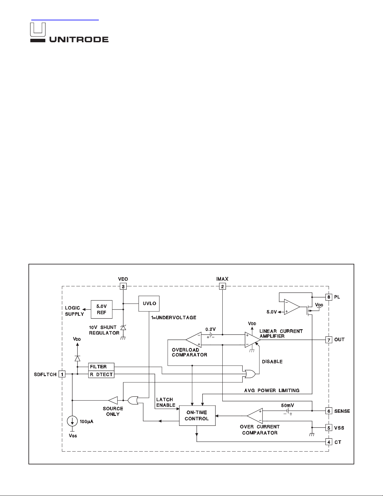
BLOCK DIAGRAM
3/98
UDG-99052
Page 2
DESCRIPTION (continued)
dropout. The fault current level is set with an external
current sense resistor, while the maximum allowable
sourcing current is programmed with a voltage divider
from VDD to generate a fixed voltage on IMAX. The current level, when the output acts as a current source, is
equal to V
start up can be programmed with a capacitor on IMAX.
When the output current is below the fault level, the output device is switched on. When the output current exceeds the fault level, but is less than the maximum
sourcing level programmed by IMAX, the output remains
switched on, and the fault timer starts charging C
IMAX/RSENSE. If desired, a controlled current
T. Once
UCC1921
UCC2921
UCC3921
C
T charges to 2.5V, the output device is turned off and
performs a retry some time later (provided that the selected mode of operation is Automatic Retry Mode).
When the output current reaches the maximum sourcing
current level, the output acts as a current source, limiting
the output current to the set value defined by IMAX.
Other features of the UCC3921 include undervoltage
lockout, 8-pin Small Outline (SOIC) and Dual-In-Line
(DIL) packages, and a Latched Operation Mode option,
in which the output is latched off once C
2.5V and stays off until either SDFLTCH is toggled (for
greater than 1ms) or the IC is powered down and then
back up.
T charges to
ABSOLUTE MAXIMUM RATINGS
IVDD..........................................50mA
SDFLTCH Current ..............................10mA
PL Current ....................................10mA
IMAX Input Voltage ..............................VDD
Storage Temperature ...................−65°C to +150°C
Junction Temperature...................–55°C to +150°C
Lead Temperature (Soldering, 10 sec.) .............+300°C
All voltages are with respect to VSS(the most negative voltage).
Currents are positive into, negative out of the specified terminal.
Consult Packaging Section of Databook for thermal limitations and
considerations of packages.
ELECTRICAL CHARACTERISTICS
for the UCC2921, and –55°C to 125°C for the UCC1921; I
resistor connected between the SDFLTCH and VSS pins. TA=TJ.
PARAMETER TEST CONDITIONS MIN TYP MAX UNITS
VDD Section
IDD 12mA
Regulator Voltage I
UVLO Off Voltage 678V
Fault Timing Section
Overcurrent Threshold T
Overcurrent Input Bias 50 500 nA
CT Charge Current V
CT Discharge Current VCT= 1V, IPL= 0 0.6 1 1.5 µA
CT Fault Threshold 2.2 2.45 2.6 V
CT Reset Threshold 0.41 0.49 0.57 V
Output Duty Cycle Fault Condition, I
Unless otherwise specified, TA= 0°C to 70°C for the UCC3921 and –40°C to 85°C
= 2mA, CT= 1nF (the minimum allowable value), there is no
VDD
SOURCE
I
SOURCE
Over Operating Temperature 46 50 53.5 mV
Overload Condition, V
= 2mA 9 9.5 10.0 V
= 10mA 9.15 9.6 10.15 V
= 25°C 47.5 50 53.5 mV
J
= 1V, IPL= 0 –50 –36 –22 µA
CT
= 0 1.7 2.7 3.7 %
PL
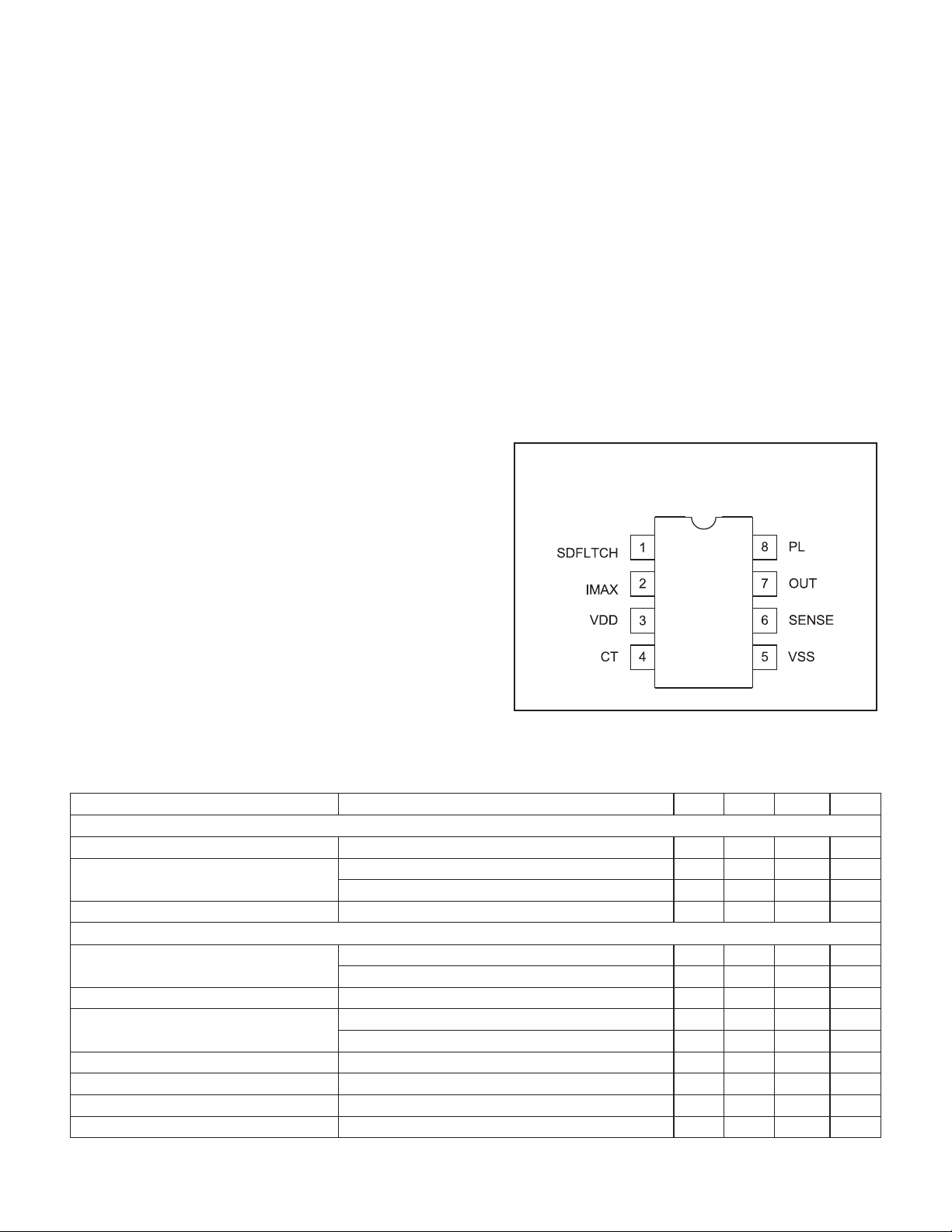
CONNECTION DIAGRAM
DIL-8 , SOIC-8 (Top View)
NorJ,DPackages
SENSE-VIMAX
= 300mV –1.7 –1.2 –0.7 mA
2
Page 3
UCC1921
UCC2921
UCC3921
ELECTRICAL CHARACTERISTICS
for the UCC2921, and –55°C to 125°C for the UCC1921; I
resistor connected between the SDFLTCH and VSS pins. TA=TJ.
PARAMETER TEST CONDITIONS MIN TYP MAX UNITS
Output Section
Output High Voltage I
Output Low Voltage I
Linear Amplifier Section
Sense Control Voltage V
Input Bias 50 500 nA
Power Limiting Section
SENSE Regulator Voltage I
V
Duty Cycle Control IPL=64µA 0.6 1.2 1.7 %
Overload Section
Delay to Output Note 1 300 500 ns
Output Sink Current V
Threshold Relative to IMAX 140 200 260 mV
Shutdown/Fault/Latch Section
Shutdown Threshold 3 5 VDD+1 V
Input Current V
Filter Delay Time (Delay to Output) 250 500 1000 µs
Fault Output High 6 9.5 V
Fault Output Low 010mV
Output Duty Cycle Fault Condition, I
Unless otherwise specified, TA= 0°C to 70°C for the UCC3921 and –40°C to 85°C
= 2mA, CT= 1nF (the minimum allowable value), there is no
VDD
= 0mA 8.5 10 V
OUT
I
= –1mA 6 8 V
OUT
= 0mA, V
OUT
I
= 2mA, V
OUT
= 100mV 85 100 115 mV
IMAX
= 400mV 370 400 430 mV
V
IMAX
=64µA 4.35 4.85 5.35 V
PL
IPL= 1mA 0.045 0.1 0.17 %
SENSE–VIMAX
SDFLTCH
I
SDFLTCH
I
SDFLTCH
SENSE–VIMAX
SENSE–VIMAX
= 300mV 40 100 mA
= 5V 50 110 250 µA
= –100µA 5 8.5 V
= 0 1.7 2.7 3.7 %
PL
= –100µA, Fault Condition, IPL=0 0 %
= 100mV 0 10 mV
= 100mV 200 600 mV
Note 1: Guaranteed by design. Not 100% tested in production.
PIN DESCRIPTIONS
CT: A capacitor is connected to this pin in order to set
the fault time. The fault time must be longer than the time
to charge external load capacitance. The fault time is
defined as:
C
•
2
T
FAULT
where ICH =36µA+IPL, and IPL is the current into the
power limit pin. Once the maximum fault time is reached
the output will shutdown for a time given by:
=• •
210
TC
SD T
IMAX: This pin programs the maximum allowable
sourcing current. Since VDD is a regulated voltage, a
voltage divider can be derived from VDD to generate the
program level for IMAX. The current level at which the
output appears as a current source is equal to the
T
=
I
CH
6
voltage on IMAX over the current sense resistor. If
desired, a controlled current start up can be programmed
with a capacitor on IMAX, and a programmed start delay
can be achieved by driving the shutdown with an open
collector/drain device into an RC network.
OUT: This pin provides gate output drive to the MOSFET
pass element.
PL: This feature ensures that the average MOSFET
power dissipation is controlled. A resistor is connected
from this pin to the drain of the NMOS pass element.
When the voltage across the NMOS exceeds 5V, current
will flow into the PL pin which adds to the fault timer
charge current, reducing the duty cycle from the 3%
level. When I
>>36µA, then the average MOSFET
PL
power dissipation is given by:
−
P avg IMAX R
MOSFET PL
=•••
110
6
3
Page 4
PIN DESCRIPTIONS (continued)
SENSE: Input voltage from the current sense resistor.
When there is greater than 50mV across this pin with
respect to VSS, then a fault is sensed, and C
charge.
SDFLTCH: This pin provides fault output indication,
shutdown control, and operating mode selection.
Interface into and out of this pin is usually performed
through level shift transistors. When open, and under a
non-fault condition, this pin pulls to a low state with
respect to VSS. When a fault is detected by the fault
timer, or undervoltage lockout, this pin will drive to a high
state with respect fo VSS, indicating the NMOS pass
element is OFF. When > 250µA is sourced into this pin
for > 1ms, it drives high causing the output to disable the
NMOS pass device.
starts to
T
UCC1921
UCC2921
UCC3921
If an 5k < R
to VSS, then the latched operating mode will be invoked.
Upon the occurrence of a fault, under the latched mode
of operation, once the C
the NMOS pass element latches off. A retry will not
periodically occur. To reset the latched off device, either
SDFLTCH is toggled high for a duration greater than 1ms
or the IC is powered down and then up.
VDD: Current driven with a resistor to a voltage approximately 10V more positive than VSS. Typically a resistor is
connected to ground. The 10V shunt regulator clamps
VDD approximately 10V above VSS, and is also used as
an output reference to program the maximum allowable
sourcing current.
VSS: Ground reference for the IC and the most negative
voltage available.
< 250kΩ resistor is placed from this pin
LATCH
capacitor charges up to 2.5V
T
APPLICATION INFORMATION
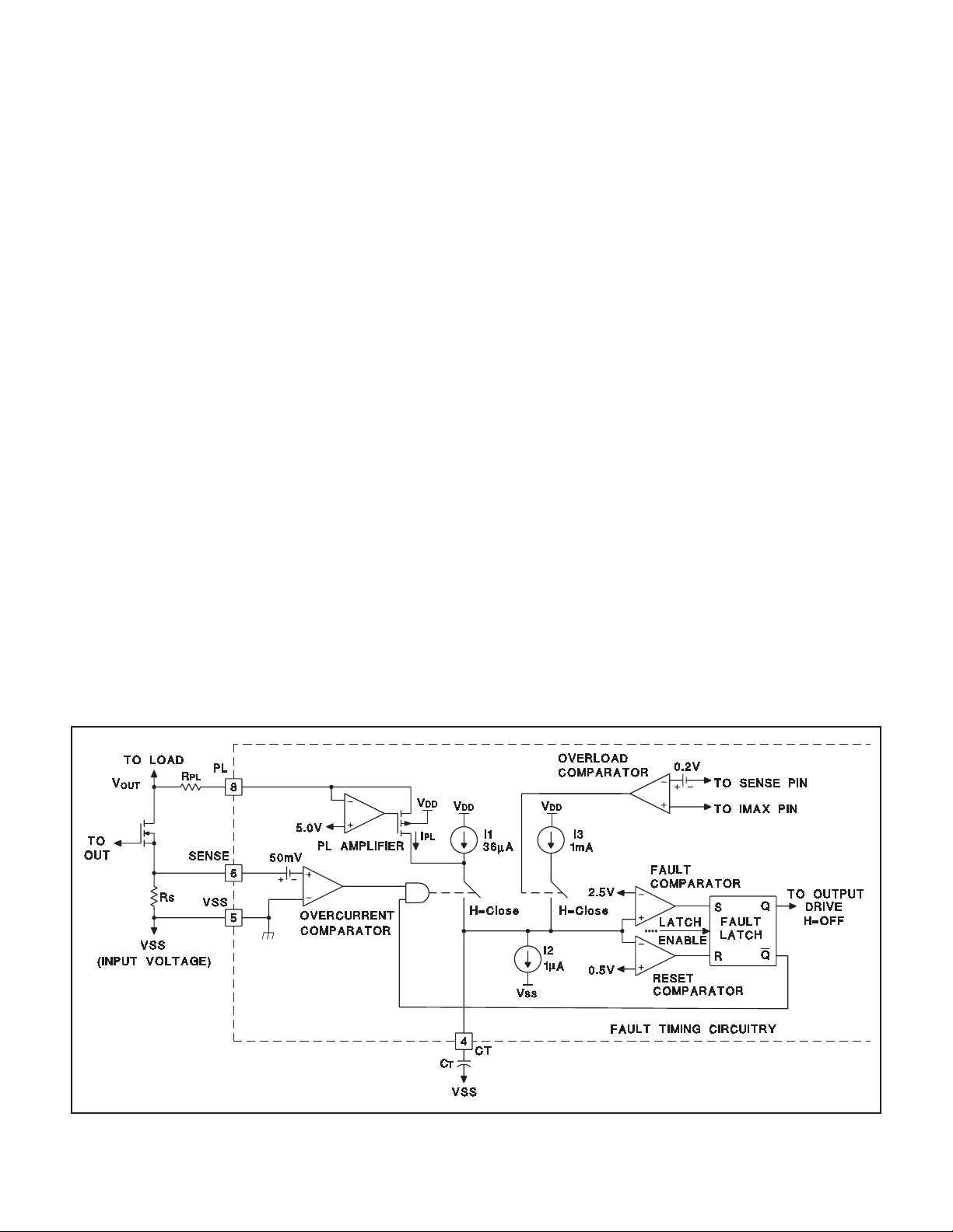
Figure 1. Fault Timing Circuitry for the UCC3921, Including Power Limit Overload
UDG-96275-1
4
Page 5

APPLICATION INFORMATION (continued)
Figure 1 shows the detailed circuitry for the fault timing
function of the UCC3921. For the time being, we will discuss a typical fault mode, therefore, the overload comparator, and current source I3 does not work into the
operation. Once the voltage across the current sense resistor, R
causes the timing capacitor to charge with a combination
of 36µA plus the current from the power limiting amplifier.
The PL amplifier is designed to only source current into
the CT pin and to begin sourcing current once the voltage across the output FET exceeds 5V. The current I
S, exceeds 50mV, a fault has occurred. This
PL
UCC1921
UCC2921
UCC3921
is related to the voltage across the FET with the following
expression:
VV
−
5
PL
FET
=
R
PL
is the voltage across the NMOS pass device.
FET
≈ VSS (input
OUT
= 0, the CT charging current is 36µA.
PL
I
where V
Later it will be shown how this feature will limit average
power dissipation in the pass device. Note that under a
condition where the output current is more than the fault
level, but less than the max level, V
voltage), I
t0: Safe condition. Output current is nominal, output
voltage is at the negative rail, VSS.
t1: Fault control reached. Output current rises above
the programmed fault value, CT begins to charge at
~36µA.
t2: Maximum current reached. Output current reaches
the programmed maximum level and becomes a constant current with value I
MAX
.
t3: Fault occurs. CT has charged to 2.5V, fault output
goes high, the FET turns off allowing no output current
to flow, V
floats up to ground.
OUT
t4: Retry. CT has discharged to 0.5V, but fault current is
still exceeded, CT begins charging again, FET is on,
pulled down towards VSS.
V
OUT
Figure 2. Retry Operation Mode
UDG-96276
t5 = t3: Illustrates 3% duty cycle.
t6 = t4: Retry. CT has discharged to 0.5V, but fault is
still exceeded, CT begins charging again, FET is on,
V
pulled down towards VSS.
OUT
t7: Output short circuit. If VOUT is short circuited to
ground, CT charges at a higher rate depending upon
the values for VSS and R
PL
.
t8: Fault occurs. Output is still short circuited, but the
occurrence of a fault turns the FET off so no current is
conducted.
t9 = t4: Output short circuit released, still in fault mode.
t10 = t0: Fault released, safe condition. Return to nor-
mal operation of the hot swap power manager.
5
Page 6

APPLICATION INFORMATION (cont.)
UCC1921
UCC2921
UCC3921
t0: Safe condition. Output current is nominal, output
voltage is at the negative rail, VSS.
t1: Fault control reached. Output current rises above
the programmed fault value, CT begins to charge at
~36µA.
t2: Maximum current reached. Output current reaches
the programmed maximum level and becomes a constant current with value I
MAX
.
t3: Fault occurs. CT has charged to 2.5V, fault output
goes high as indicated by the SDFLTCH voltage. The
FET turns off allowing no output current to flow, V
OUT
floats up to ground, and since there is an 82kΩ resistor
from the SDFLTCH pin to VSS, the internal latchset signal goes high.
t4: Since the user does not want the chip to LATCH off
during this cycle, he toggles SDFLTCH high for greater
than 1ms {t6 - t4 > 1ms}.
t5: The latchset signal is reset.
t6: Forcing of SDFLTCH is released after having been
applied for > 1ms.
t7: Retry (since the latchset signal has been reset to its’
low state) - CT has discharged to 0.5V, but fault current
UDG-96277
is still exceeded, CT begins charging again, FET is on,
V
pulled down towards VSS.
OUT
t8 = t3: Fault occurs. CT has charged to 2.5V, fault output goes high as indicated by the SDFLTCH voltage,
the FET turns off allowing no output current to flow,
floats up to ground, and since there is an 82kΩ
V
OUT
resistor from SDFLTCH to VSS, the internal latchset
signal goes high.
t9: Output is latched off. Even though CT has discharged to 0.5V, there will not be a retry since the
latchset signal was allowed to remain high.
t10: Output remains latched off. CT has discharged all
thewayto0V.
t11: The output has been latched off for quite some
time. The user now wishes to reset the latched off output, thus toggling SDFLTCH high for greater than 1ms
{t13 - t11}.
t12 = t5: The latchset signal is reset.
t13: Forcing of SDFLTCH is released after having been
applied for > 1ms. The fault had also been released
during the time the output was latched off, safe condition, return to normal operation of the hot swap power
manager.
Figure 3. Latched Operation Mode: R
LATCH
= 82k
6
Page 7

APPLICATION INFORMATION (continued)
During a fault, CT will charge at a rate determined by the
internal charging current and the external timing capacitor. Once CT charges to 2.5V, the fault comparator
switches and sets the fault latch. Setting of the fault latch
causes both the output to switch off and the charging
switch to open. CT must now discharge with the 1µA current source, I2, until 0.5V is reached. Once the voltage at
CT reaches 0.5V, the fault latch resets, which re-enables
the output and allows the fault circuitry to regain control
of the charging switch. If a fault is still present, the fault
comparator will close the charging switch causing the cycle to repeat. Under a constant fault, the duty cycle is
given by:
A
1
Duty Cycle
Average power dissipation in the pass element is given
by:
PVI
Where V
V
R
=••
FET FET MAX
AVG
>>5V IPLcan be approximated as:
FET
FET
PL
and where IPL>>36µA, the duty cycle can be approximated as :
1
µAR
•
PL
V
FET
Therefore, the maximum average power dissipation in
the MOSFET can be approximated by:
PVI
FET FET MAX
=••
=••
AVG
IMAX A R
µ
1
Notice that in the approximation, V
limiting the average power dissipation in the NMOS pass
element.
Overload Comparator
The linear amplifier in the UCC3921 ensures that the
output NMOS does not pass more than I
V
IMAX/RSENSE
). In the event the output current exceeds
the programmed I
occur if the output FET is not responding to a command
from the IC, CT will begin charging with I3, 1mA, and
continue to charge to approximately 8V. This allows a
constant fault to show up on the SDFLTCH pin, and also
since the voltage on CT will continue charging past 2.5V
in an overload fault mode, it can be used for detection of
µ
=
IA
+
µ
36
PL
1
µ
IA
+
PL
AR
•
1
µ
V
FET
PL
by 0.2V/R
MAX
A
µ
36
PL
FET
SENSE,
cancels, thereby
(which is
MAX
which can only
UCC1921
UCC2921
UCC3921
output FET failure or to build redundancy into the system.
Determining External Component Values
To set R
V
IN
R
Figure 4.
In order to estimate the minimum timing capacitor, CT,
several things must be taken into account. For example,
given the schematic in Figure 4 as a possible (and at this
point, a standard) application, certain external component values must be known in order to estimate C
Now, given the values of C
the resistors determining the voltage on the IMAX pin,
the user can calculate the approximate startup time of
the node V
time it takes for CTto charge to 2.5V (relative to VSS),
and is the basis for estimating the minimum value of C
In order to determine the value of the sense resistor,
R
SENSE
rent, R
R
SENSE
Next, the variable I
maximum current that the UCC3921 will allow through
the transistor, M1, and it can be shown that during
startup with an output capacitor the power MOSFET, M1,
can be modeled as a constant current source of value
where
I
MAX
I
MAX
Given this information, calculation of the startup time is
now possible via the following:
(see Fig. 4) the following must be achieved:
VDD
min
VDD
V
10
>
RR
+
12
This startup time must be faster than the
OUT.
mA
+
2
, Load, R
OUT
SENSE,VSS
UDG-96278
, and
, assuming the user has determined the fault cur-
can be calculated by:
SENSE
mV
50
=
I
FAULT
=
V
IMAX
R
SENSE
must be calculated. I
MAX
where V
= voltage on pin IMAX.
IMAX
MAX
is the
TMIN
.
.
T
7
Page 8

APPLICATION INFORMATION (continued)
Current Source Load:
CV
•
T
START
Resistive Load:
T
START
CR n
OUT OUT
Once T
START
UCC3921 must be addressed and component values derived. Assuming the user chooses to limit the maximum
25
22.5
20
17.5
15
12.5
10
7.5
5
2.5
0
Figure 5. Plot Average Power vs FET Voltage for
Increasing Values of R
OUT SS
=
II
−
MAX LOAD
=
••
l
IR
•
MAX OUT
IR V
•−
MAX OUT SS
is calculated, the power limit feature of the
R
I=4AMAX
R
R
R
R
R
R
0 25 50 75 100 125 150 175 200
FET
V
PL
= ∞
PL= ∞
= ∞
PL =10M
PL =5M
PL =2M
PL =1M
PL
=500k
=200k
PL
UCC1921
UCC2921
UCC3921
Resistive Load:
C
min
=
T
TARVVIR
•••+−−•
336 5
START PL SS MAX OUT
R
•
3
UT SS OUT
O
+
Level Shift Circuitry to Interface with SDFLTCH
Some type of circuit is needed to interface with the
UCC3921 via SDFLTCH, such as opto-couplers or level
shift circuitry. Figure 6 depicts one implementation of
level shift circuitry that could be used, showing component values selected for a typical –48V telecommunications application. There are three communication
conditions which could occur; two of which are Hot Swap
Power Manager (HSPM) state output indications, and the
third being an External Shutdown.
1) When open, and under a non-fault condition,
SDFLTCH is pulled to a low state. In Figure 6, the Nchannel level shift transistor is off, and the
FAULT OUT
R3. This indicates that the HSPM is not faulted.
2) When a fault is detected by the fault timer or undervoltage lockout, this pin will drive to a high state, indicating that the external power FET is off. In Figure 6,
the N-channel level shift transistor will conduct, and
the FAULT OUT
ode voltage drop below LOCAL GND. This indicates
that the HSPM is faulted. The Schottky Diode is necessary to ensure that the FAULT OUT
not traverse too far below LOCAL GND, making fault
detection difficult.
µ
()
5
R
•
PL
VC
••
5
R
•
PL
signal is pulled to LOCAL VDD through
signal will be pulled to a Schottky Di-
signal does
allowable average power that will be associated with the
hot swap power manager, the power limiting resistor,
PL, can be easily determined by the following:
R
Pavg
R
=
PL
defined by
FET
AI
•1µ
R
where a minimum RPLexists
MAX
V
SS
PL
min
=
(Refer to Figure 5).
5
mA
Finally, after computing the aforementioned variables, the
minimum timing capacitor can be derived as such:
Current Source Load:
C
min
=
T
TARVV
•••+−
372 10
START PL SS
µ
()
10
R
•
PL
UDG-96279
Figure 6. Possible Level Shift Circuitry to
Interface to the UCC3921, showing component
values selected for a typical telecom application.
8
Page 9

APPLICATION INFORMATION (continued)
If a5k<R
SDFLTCH & VSS, as optionally shown in Figure 6,
then the latched operating mode (described earlier)
will be invoked upon the occurrence of a fault.
3) To externally shutdown the HSPM, the SHUTDOWN
signal (typically held at LOCAL VDD) must be pulled
to LOCAL GND. Assuming SHUTDOWN is tied to
LOCAL GND, the P-channel level shift transistor will
conduct, driving SDFLTCH high (to roughly VDD plus
a diode). By sourcing > 250µA into SDFLTCH for >
1ms the output to the external power FET will be disabled. The current sourced into SDFLTCH must be
< 250kΩ resistor is tied between
LATCH
UCC1921
UCC2921
UCC3921
limited to 10mA or less: I
SDFLTCHMAX < 10mA.
SAFETY RECOMMENDATIONS
Although the UCC3921 is designed to provide system
protection for all fault conditions, all integrated circuits
can ultimately fail short. For this reason, if the UCC3921
is intended for use in safety critical applications where
or some other safety rating is required, a redundant
UL
safety device such as a fuse should be placed in series
with the external power FET. The UCC3921 will prevent
the fuse from blowing for virtually all fault conditions, increasing system reliability and reducing maintenance
cost, in addition to providing the hot swap benefits of the
device.
Figure 7. Typical Telecommuications Application
(The “Negative Magnitude-Side” of the Supply is Switched in)
Ω
UDG-98053
9
Page 10

APPLICATION INFORMATION (continued)
UCC1921
UCC2921
UCC3921
Figure 8. Floating Positive Application
The “Ground-side” of the Supply is Switched In
Ω
UDG-98054
UNITRODE CORPORATION
7 CONTINENTAL BLVD. •MERRIMACK, NH 03054
TEL. (603) 424-2410 • FAX (603) 424-3460
10
Page 11

IMPORTANT NOTICE
T exas Instruments and its subsidiaries (TI) reserve the right to make changes to their products or to discontinue
any product or service without notice, and advise customers to obtain the latest version of relevant information
to verify, before placing orders, that information being relied on is current and complete. All products are sold
subject to the terms and conditions of sale supplied at the time of order acknowledgement, including those
pertaining to warranty, patent infringement, and limitation of liability.
TI warrants performance of its semiconductor products to the specifications applicable at the time of sale in
accordance with TI’s standard warranty. Testing and other quality control techniques are utilized to the extent
TI deems necessary to support this warranty . Specific testing of all parameters of each device is not necessarily
performed, except those mandated by government requirements.
CERTAIN APPLICATIONS USING SEMICONDUCTOR PRODUCTS MAY INVOLVE POTENTIAL RISKS OF
DEATH, PERSONAL INJURY, OR SEVERE PROPERTY OR ENVIRONMENTAL DAMAGE (“CRITICAL
APPLICATIONS”). TI SEMICONDUCTOR PRODUCTS ARE NOT DESIGNED, AUTHORIZED, OR
WARRANTED TO BE SUITABLE FOR USE IN LIFE-SUPPORT DEVICES OR SYSTEMS OR OTHER
CRITICAL APPLICA TIONS. INCLUSION OF TI PRODUCTS IN SUCH APPLICATIONS IS UNDERST OOD TO
BE FULLY AT THE CUSTOMER’S RISK.
In order to minimize risks associated with the customer’s applications, adequate design and operating
safeguards must be provided by the customer to minimize inherent or procedural hazards.
TI assumes no liability for applications assistance or customer product design. TI does not warrant or represent
that any license, either express or implied, is granted under any patent right, copyright, mask work right, or other
intellectual property right of TI covering or relating to any combination, machine, or process in which such
semiconductor products or services might be or are used. TI’s publication of information regarding any third
party’s products or services does not constitute TI’s approval, warranty or endorsement thereof.
Copyright 1999, Texas Instruments Incorporated
 Loading...