

Page 1

1
FEATURES
DESCRIPTION
APPLICATIONS
UCC28230
UCC28231
www.ti.com
................................................................................................................................................... SLUS814A – FEBRUARY 2008 – REVISED JUNE 2008
Advanced PWM Controller for Bus Converters
• Programmable, Load Depended Off Time
Control
The UCC28230, UCC28231 PWM bus controllers are
optimized for use in high efficiency, high power
• Frequency Controlled Start Up Allows Small
density, unregulated intermediate bus converters.
Output Inductor, Low Ripple and Constant
Topologies include push-pull, half-bridge and
Current Start with Large Output Capacitor
full-bridge. External drivers, such as the UCC27200
• Two 0.2-A Push-Pull Outputs Provide Matched
120-V high-side/low-side drivers, can be used with
Control Signals D to External Drivers
this controller.
• Two Additional 1- D Outputs for Optimal Use
Low cost, small size and highly efficient solutions are
of Self-Driven or Control Driven Synchronous
provided by innovations such as:
Rectifiers
• Start-up frequency control circuit allowing small
• Unregulated, Fixed Volt-Second or Fixed
output inductor and the ability to start with large
Frequency Modes set by User
intermediate bus capacitor.
• Two, 1.5% Overall Accuracy Reference Voltage
• Load depended off-time control set by user.
Options: 5-V for UCC28230 and 3.3-V for
Additional 1-D control outputs can be used for
UCC28231
primary winding clamping in self-driven output
• Resistor Programmable Switching Frequency
synchronous rectifier applications or as drive signals
up to 1 MHz
for the control-driven synchronous rectifier.
• Cycle-by-Cycle Current Limit Allows Parallel
Cycle-by-cycle current limit prevents overstresses of
Operation with Droop Based Current Sharing
converter. If the over current condition causes less
than 80% duty cycle at the output, then after a
• Single External Capacitor sets Soft-Start and
programmed time the controller proceeds into
Over Current Hiccup Mode Parameters with
periodical shutdown and restart hiccup mode.
Restart
The UCC28230 provides 5 V, and the UCC28231
• Severe Short Circuit Hiccup with Restart or
provides 3.3-V precision reference voltages with 1.5%
Latch Off Protection Option by External
overall accuracy and 10-mA output current. This
Resistor
reference voltage can be used to supply
• Input Under Voltage Lock Out
housekeeping circuit and/or microcontroller. The
• Thermal Shutdown
precision reference voltage can also be used for
accurate setting of system parameters.
• Thermally Enhanced 3 mm × 2 mm SON-12
and TSSOP-14 Package Options
Other features include under-voltage lockout, thermal
shut down, programmable soft start, over-current
hiccup mode and short circuit protection with internal
restart by default that can be set into latch-off mode
• Intermediate Bus Isolated Converters
by an external resistor.
• DC-to-DC Transformers
1
Please be aware that an important notice concerning availability, standard warranty, and use in critical applications of Texas
Instruments semiconductor products and disclaimers thereto appears at the end of this data sheet.
PRODUCTION DATA information is current as of publication date.
Copyright © 2008, Texas Instruments Incorporated
Products conform to specifications per the terms of the Texas
Instruments standard warranty. Production processing does not
necessarily include testing of all parameters.
Page 2
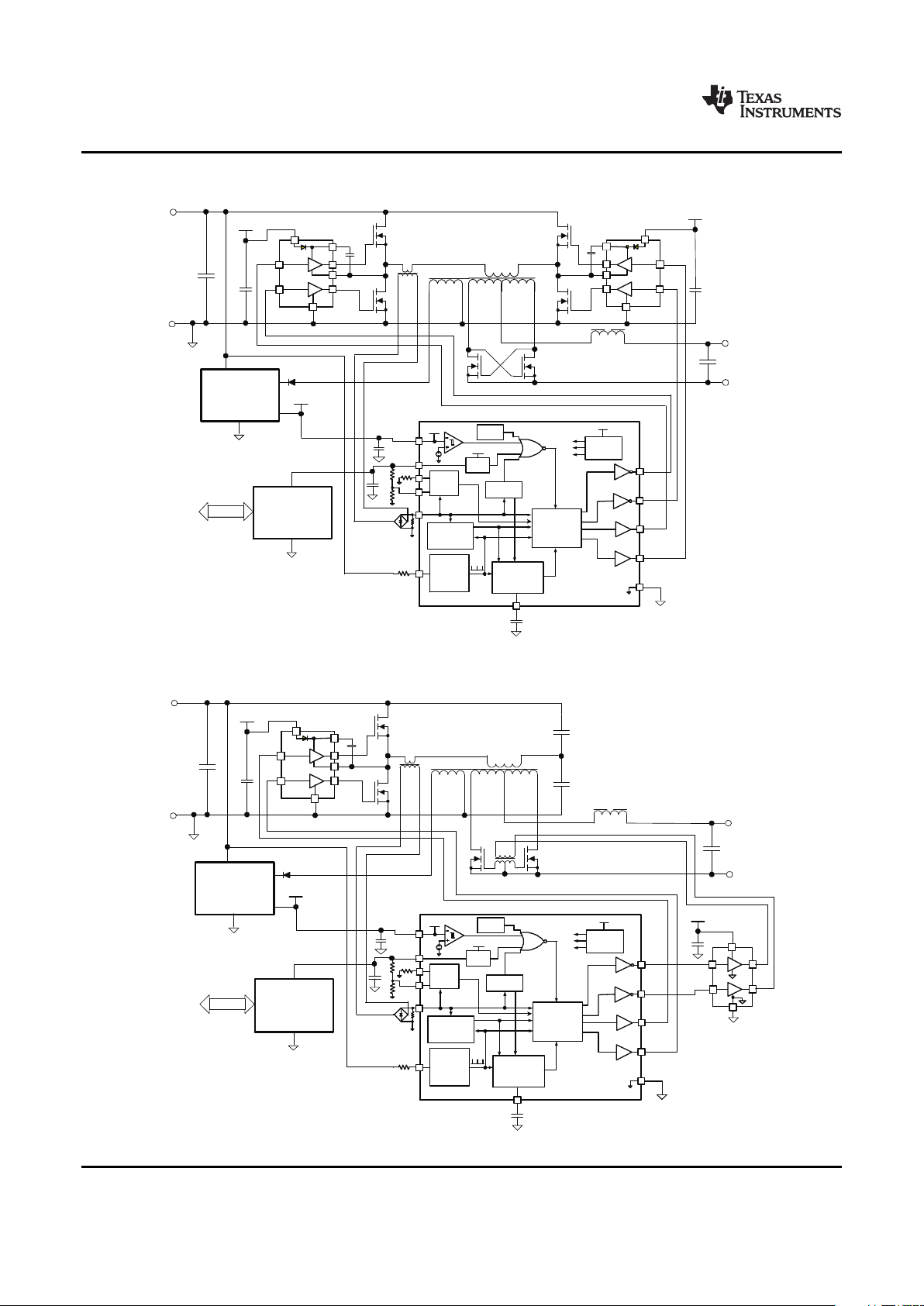
TYPICAL APPLICATION DIAGRAMS
Vin
36 Vto60V
+
_
CT
Vout
7 Vto12 V
400W
+
_
Vbias
Vbias
Vcc=5 Vor3.3V
Interface
with
System
HI
V
DD
V
SS
LI
HB
HO
HS
LO
HI
V
DD
V
SS
LI
HB
HO
HS
LO
UCC27200UCC27200
Bias
Power
Supply
Vbias
Housekeeping
Micro
Controller
GND
O1_D
VREF
V
DD
5V/3.3V
LDO
EN
UVLO
Comp.
6.3Vrise
5.7 Vfall
V
DD
V
DD
RT
CS
SS
Vin
OS
Thermal
Shutdown
Is
R1
R2
O2_DIN
O2_D
O1_DIN
8
10
11
9
7
1
2
6
4
12
SoftStart
&
HiccupCurrent
LimitCircuit
Logic
Block
V
DD
Reference
Generator
ShortCircuit
Shutdown
Oscillator
&
StartUp
Frequency
Control
Off Time
Control
Circuit
Cycle-by
-
CycleCurrent
Limit
CLK
3
OST
R3
5
Vin
36Vto60V
+
_
CT
Vout
7Vto12V
200W
+
_
Vbias
Houskeeping
Micro-
Controller
Vcc=5Vor3.3V
Interface
with
System
HI
V
DD
V
SS
LI
HB
HO
HS
LO
UCC27200
Bias
Power
Supply
Vbias
UCC28230/1
INA
2
4
7
5
6
3
V
DD
GND
INB
UCC27324
OUTA
OUTB
Vbias
GND
O1_D
VREF
V
DD
5V/3.3V
LDO
EN
UVLO
Comp.
6.3Vrise
5.7 Vfall
V
DD
V
DD
RT
CS
SS
Vin
OS
Thermal
Shutdown
Is
R1
R2
O2_DIN
O2_D
O1_DIN
8
10
11
9
7
1
2
6
4
12
SoftStart
&
HiccupCurrent
LimitCircuit
Logic
Block
V
DD
Reference
Generator
ShortCircuit
Shutdown
Oscillator
&
StartUp
Frequency
Control
Off Time
Control
Circuit
Cycle -by -
CycleCurrent
Limit
CLK
3
OST
R3
5
UCC28230
UCC28231
SLUS814A – FEBRUARY 2008 – REVISED JUNE 2008 ...................................................................................................................................................
www.ti.com
Figure 1. Full-Bridge Bus Converter
Figure 2. Half-Bridge Bus Converter with Control-Driven Synchronous Rectifier
2 Submit Documentation Feedback Copyright © 2008, Texas Instruments Incorporated
Product Folder Link(s): UCC28230 UCC28231
Page 3

PINOUT CONFIGURATION
UCC28230
UCC28231
www.ti.com
................................................................................................................................................... SLUS814A – FEBRUARY 2008 – REVISED JUNE 2008
ORDERING INFORMATION
(1) (2)
TEMPERATURE RANGE,
REFERENCE VOLTAGE PACKAGE TAPE and REEL QTY PART NUMBER
TA= T
J
5 V .250 UCC28230DRNT
5 V 3000 UCC28230DRNR
Plastic 12-pin SON (DRN)
3.3 V 250 UCC28231DRNT
3.3 V 3000 UCC28231DRNR
– 55 ° C to +125 ° C
5 V 250 UCC28230PW
5 V 2000 UCC28230PWR
Plastic 14-pin TSSOP (PW)
3.3 V 250 UCC28231PW
3.3 V 2000 UCC28231PWR
(1) The 12-pin SON (DRN) and 14-pin TSSOP packages use Pb-Free lead finish of Pd-Ni-Au which is compatible with MSL level 1 at
255-260 ° C peak reflow temperature to be compatible with either lead free or Sn/Pb soldering operations.
(2) The pad underneath the center of the IC is a thermal substrate. The PCB “ thermal land ” design for this exposed die pad should include
thermal vias that drop down and connect to one or more buried copper plane(s). This combination of vias for vertical heat escape and
buried planes for heat spreading allows the DRN to achieve its full thermal potential. This pad is also internally connected to GND pin.
Copyright © 2008, Texas Instruments Incorporated Submit Documentation Feedback 3
Product Folder Link(s): UCC28230 UCC28231
Page 4
ABSOLUTE MAXIMUM RATINGS
DISSIPATION RATINGS
(1)
RECOMMENDED OPERATING CONDITIONS
UCC28230
UCC28231
SLUS814A – FEBRUARY 2008 – REVISED JUNE 2008 ...................................................................................................................................................
www.ti.com
over operating free-air temperature range
(1) (2)
(unless otherwise noted)
PARAMETER VALUE UNIT
V
DD
(3)
Input supply voltage range – 0.3 to 20.0
O1_D, O2_D, O1_DIN, O2_DIN – 0.3 to V
DD
+0.3
Inputs voltages on OS, CS, SS, RT, OST – 0.3 to 6.3
V
Output voltage on VREF – 0.3 to 5.6
HBM 2k
ESD rating
CDM 500
Continuous total power dissipation See Dissipation Rating Table
T
J
Operating virtual junction temperature range – 55 to +150
T
A
Operating ambient temperature range – 55 to +125
° C
T
stg
Storage Temperature – 65 to +150
Lead Temperature (Soldering, 10 sec.) PW Package +300
(1) Stresses beyond those listed under absolute maximum ratings may cause permanent damage to the device. These are stress ratings
only, and functional operation of the device at these or any other conditions beyond those indicated under recommended operating
conditions is not implied. Exposure to absolute-maximum-rated conditions for extended periods may affect device reliability.
(2) These devices are sensitive to electrostatic discharge; follow proper device handling procedures.
(3) All voltages are with respect to GND unless otherwise noted. Currents are positive into, negative out of the specified terminal. See
Packaging Section of the datasheet for thermal limitations and considerations of packages.
θJC( ° C/W) θJA( ° C/W) θJB( ° C/W)
θJP( ° C/W)
BOARD PACKAGE JUNCTION TO JUNCTION TO JUNCTION TO
JUNCTION TO PAD
CASE AMBIENT BOARD
High-K
(2)
DRN 70.66 15 37.66
PW 2.71 97.65 2.07
(1) These thermal data are taken at standard JEDEC test conditions and are useful for the thermal performance comparison of different
packages. The cooling condition and thermal impedance R
θ JA
of practical design is specific.
(2) The JEDEC test board JESD51-5 with direct thermal pad attach, 3-inch × 3-inch, 4-layer with 1-oz internal power and ground planes and
2-oz top and bottom trace layers (preliminary data based on modeling)
MIN NOM MAX UNIT
V
DD
Supply voltage range 7 12 17 V
Operating junction temperature range – 55 125 ° C
4 Submit Documentation Feedback Copyright © 2008, Texas Instruments Incorporated
Product Folder Link(s): UCC28230 UCC28231
Page 5
ELECTRICAL CHARACTERISTICS
(1)
UCC28230
UCC28231
www.ti.com
................................................................................................................................................... SLUS814A – FEBRUARY 2008 – REVISED JUNE 2008
V
DD
= 12V, 1- µ F capacitor from V
DD
and VREF to GND, TA= TJ= – 55 ° C to 125 ° C, RT = 49.9 k Ω connected to 4.4V supply to
set Fsw = 100 kHz (unless otherwise noted).
PARAMETER TEST CONDITIONS MIN TYP MAX UNIT
Supply Currents
ID
DD(off)
Startup current VDD= 5.2 V 150 200 µ A
I
DD
Operating supply current 1.5 2.5 mA
Under Voltage Lockout
Start threshold 5.9 6.3 6.9
Minimum operating voltage after start 5.3 5.7 6.2 V
Hysteresis 0.55 0.6 0.75
Soft Start (SS PIN, Figure 41 , Figure 44 )
I
SS
Charge current VSS= 0 V – 30 – 25 – 20 µ A
V
SS_STD
Shutdown/restart/reset threshold 0.3 0.55 0.68
V
SS_FP
Soft-start first pulse threshold 0.68 0.85 1.1
V
V
SS_PU
Pull up threshold 3.3 3.5 3.8
V
SS_CL
Clamp voltage 4.3 4.5 4.8
Off-Time Programming (Figure 33 )
T
OFF5
Off time between O1_D and O2_D UCC28230 32 40 50
T
OFF3
Off time between O1_D and O2_D UCC28231 30 40 53
OS = 8.45 k Ω , CS = 0.3 V, OST = 1 V
T
DT
Dead time between O1_D, O1_DIN and O2_D, O2_DIN 10 16
Δ T
OFF
Off time matching 2
ns
T
OFFR5
Off time between O1_D and O2_D UCC28230 32 40 50
T
OFFR3
Off time between O1_D and O2_D UCC28231 30 40 53
OS = 8.45 k Ω , CS = 0 V, OST = VREF
T
DTREF
Dead time between O1_D, O1_DIN and O2_D, O2_DIN 10 16
Δ T
OFFR
Off time matching 2
I
HYST
Hysteresis current source 10 µ A
OS = 8.45 k Ω , OST = 1 V, CS = CS
TH
– 0.03
T
OFFMAX
Maximum off time at low CS 165 235 ns
V
Switching Frequency at O1_D and O2_D Outputs
F
SWNOM
Nominal frequency VSS= 4 V 92 100 108
kHz
F
SWMAX
Maximum frequency VSS= 1.8 V 425 550 675
VREF Output Voltage
V
REF5
UCC28230 4.925 5 5.075
0 ≤ IR ≤ 10 mA; VDD= from 7 V to 17 V,
VREF total output range V
– 55 ° C ≤ TJ≤ 125 ° C
V
REF3
UCC28231 3.25 3.3 3.35
I
SCC
Short circuit current VREF = 0 V – 35 – 25 – 12 mA
(1) Typical values for TA= 25 ° C
Copyright © 2008, Texas Instruments Incorporated Submit Documentation Feedback 5
Product Folder Link(s): UCC28230 UCC28231
Page 6
UCC28230
UCC28231
SLUS814A – FEBRUARY 2008 – REVISED JUNE 2008 ...................................................................................................................................................
www.ti.com
ELECTRICAL CHARACTERISTICS (continued)
V
DD
= 12V, 1- µ F capacitor from V
DD
and VREF to GND, TA= TJ= – 55 ° C to 125 ° C, RT = 49.9 k Ω connected to 4.4V supply to
set Fsw = 100 kHz (unless otherwise noted).
PARAMETER TEST CONDITIONS MIN TYP MAX UNIT
Current Sense, Cycle-by-Cycle Current Limit With Hiccup, Short Circuit Protection With Latch Off
V
CS_LIM
CS pin cycle-by-cycle threshold 0.48 0.5 0.515 V
Input pulse at CS from 0.3 V to 0.6 V with
T
CS
CS to O1_D and O2_D propagation delay 100
0.03 V/ns slew rate
ns
Input pulse at CS from 0.3 V to 0.6 V with
T
BL
Leading edge blanking time by internal filter 50
0.03 V/ns slew rate
Discharge current to set cycle-by-cycle current limit duration
I
DS
CS = 0.6 V, VSS= 4 V 15 20 25 µ A
(Figure 41 )
Hiccup OFF time threshold 3.1 3.4 3.7 V
Discharge current to set Hiccup Mode OFF Time
I
HCC
1.9 2.5 3.1 µ A
(Figure 41 , Figure 44 )
V
CS_SC
CS pin short circuit protection threshold (Figure 44 ) 0.65 0.7 0.75 V
Outputs O1_D, O2_D, O1_DIN, O2_DIN
Sink/Source peak current
(2)
0.2 A
Rise time C
LOAD
= 100 pF 12 25
ns
Fall time C
LOAD
= 100 pF 10 25
RSRC Output source resistance I
OUT
= 20 mA 10 20 35
Ω
RSINK Output sink resistance I
OUT
= 20 mA 5 15 30
Pins 7 and 9 pulses matching at FSW= 100
Duty cycle matching 35 ns
kHz
Thermal Shutdown
Rising threshold
(3)
150 160 170
Falling threshold
(3)
130 140 150 ° C
Hysteresis 20
(2) Output sink/source peak current value, defined by equation IP= 100 pF × dV/dt where dV/dt is taken from the output rise and fall
switching waveforms. It is not tested in production. Characterization is available upon request.
(3) Thermal shutdown is not tested in production. Characterization is available upon request
6 Submit Documentation Feedback Copyright © 2008, Texas Instruments Incorporated
Product Folder Link(s): UCC28230 UCC28231
Page 7

FUNCTIONAL BLOCK DIAGRAMS
GND
O1_D
VREF
V
DD
5V/3.3V
LDO
EN
UVLO
Comp.
6.3V rise
5.7V fall
V
DD
V
DD
RT
CS
SS
Vin
CT
OS
Thermal
Shutdown
Is
R1
R2
O2_DIN
O2_D
O1_DIN
8
10
11
9
7
5
1
2
6
4
12
Soft Start &
Hiccup Current
Limit Circuit
Logic
Block
V
DD
Reference
Generator
Short Circuit
Shutdown
Oscillator &
Start Up
Frequency
Control
Off Time
Control
Circuit
Cycle-by-
Cycle Current
Limit
CLK
3
OST
R3
GND
O1_D
VREF
V
DD
5V/3.3V
LDO
EN
UVLO
Comp.
6.3V rise
5.7V fall
V
DD
V
DD
RT
CS
SS
Vin
CT
OS
Thermal
Shutdown
Is
R1
R2
O2_DIN
O2_D
O1_DIN
10
12
13
11
9
6
1
2
7
5
14
Soft Start &
Hiccup Current
Limit Circuit
Logic
Block
V
DD
Reference
Generator
Short Circuit
Shutdown
Oscillator &
Start Up
Frequency
Control
Off Time
Control
Circuit
Cycle-by-
Cycle Current
Limit
CLK
3
OST
R3
AGND
8
NC
4
UCC28230
UCC28231
www.ti.com
................................................................................................................................................... SLUS814A – FEBRUARY 2008 – REVISED JUNE 2008
Figure 3. SON-12 Package
Figure 4. TSSOP-14 Package
Copyright © 2008, Texas Instruments Incorporated Submit Documentation Feedback 7
Product Folder Link(s): UCC28230 UCC28231
Page 8

UCC28230
UCC28231
SLUS814A – FEBRUARY 2008 – REVISED JUNE 2008 ...................................................................................................................................................
www.ti.com
TERMINAL FUNCTIONS
TERMINAL
I/O FUNCTION
DFN-12 TSSOP-14
NAME
PIN# PIN#
± 1.5% accurate 5 V for UCC28230 and 3.3 V for UCC28231, 10-mA output reference voltage with
short circuit protection that can be used for fixed switching frequency setting and/or for
1 1 VREF O
housekeeping microcontroller. Place decoupling capacitor in 1 µ F to 2.2 µ F range from this pin to
GND.
Off time control threshold pin uses a resistor divider to set current level as percentage of current
2 2 OST I
limit threshold.
Nominal off time T
OFF
and dead time TDTset pin. An external resistor connected between this pin
3 3 OS I
and GND sets the dead time and nominal off time.
4 NC Not connected pin, TSSOP-14 only.
Oscillator timing input pin. The external resistor which is connected between this pin and VINsets
4 5 RT I the oscillator frequency which varies with VIN. Tying the external resistor to VREF sets fixed
frequency operation independent of VIN.
Input to adjustable soft-start,and hiccup mode circuit. Place soft-start capacitor from this pin to
5 6 SS I/O GND. The internal charge/discharge current ISSand an external capacitor value set the soft-start
timing, duration of cycle-by-cycle current limit and controller turn-off time for hiccup mode operation.
6 7 CS I Current sensing pin used for cycle-by-cycle current limit, short circuit protection and off time control.
8 AGND Analog ground, TSSOP-14 only.
7 9 GND Ground pin connected to thermal pad. All signals are referenced to this node.
8 10 O2_DIN O 0.2-A sink/source switching output pin to an external driver providing 1-D pulse.
9 11 O2_D O 0.2-A sink/source switching output pin to an external driver providing D pulse.
10 12 O1_DIN O 0.2-A sink/source switching output pin to an external driver providing 1-D pulse.
11 13 O1_D O 0.2-A sink/source switching output pin to an external driver providing D pulse.
Connect this pin to a 7-V to 17-V bias supply. Place a high quality at least 1- µ F ceramic bypass
12 14 VDD I
capacitor from this pin to GND.
8 Submit Documentation Feedback Copyright © 2008, Texas Instruments Incorporated
Product Folder Link(s): UCC28230 UCC28231
Page 9
TYPICAL CHARACTERISTICS
Operating Supply Current I
DD
over Temperature at FSW=100kHz
1.40
1.45
1.50
1.55
1.60
-55 -35 -15 5 25 45 65 85 105 125
TJ-tempe rature, °C
I
DD,
mA
Start-up Current I
DDoff
over Temperature at VDD=5.2V
135
140
145
150
155
160
165
-55 -35 -15 5 25 45 65 85 105 125
TJ-tempera ture, °C
I
DDo ff,,
µA
Under Voltage Lockout Thresholds
over Temperature
5.3
5.5
5.7
5.9
6.1
6.3
6.5
6.7
-55 -35 -15 5 25 45 65 85 105 125
TJ-temperature, °C
UVLO Thresholds, V
Rising threshold
Falling threshold
Under Voltage Lockout Hysteresis
over Temperature
0.62
0.64
0.66
0.68
0.70
-55 -35 -15 5 25 45 65 85 105 125
TJ-temperature, °C
UVLO Hysteresis, V
Soft Start Shutdown V
SS_STD
and First Pulse V
SS_FP
Thresholds over Temperature
0.30
0.40
0.50
0.60
0.70
0.80
0.90
1.00
-55 -35 -15 5 25 45 65 85 105 125
TJ-te mperature, ° C
V
SS_STD
, V
SS_FP
, V
Soft Start Shutdown
First Puls e Threshold
Soft Start Pull-up V
SS_PU
and Clamp Voltage V
SS_CL
Thresholds over Temperature
3.00
3.50
4.00
4.50
5.00
-55 -35 -15 5 25 45 65 85 105 125
TJ-te mperature, ° C
V
SS_PU
, V
SS_CL
, V
Pull-up Threshold
Clamp Voltage
UCC28230
UCC28231
www.ti.com
................................................................................................................................................... SLUS814A – FEBRUARY 2008 – REVISED JUNE 2008
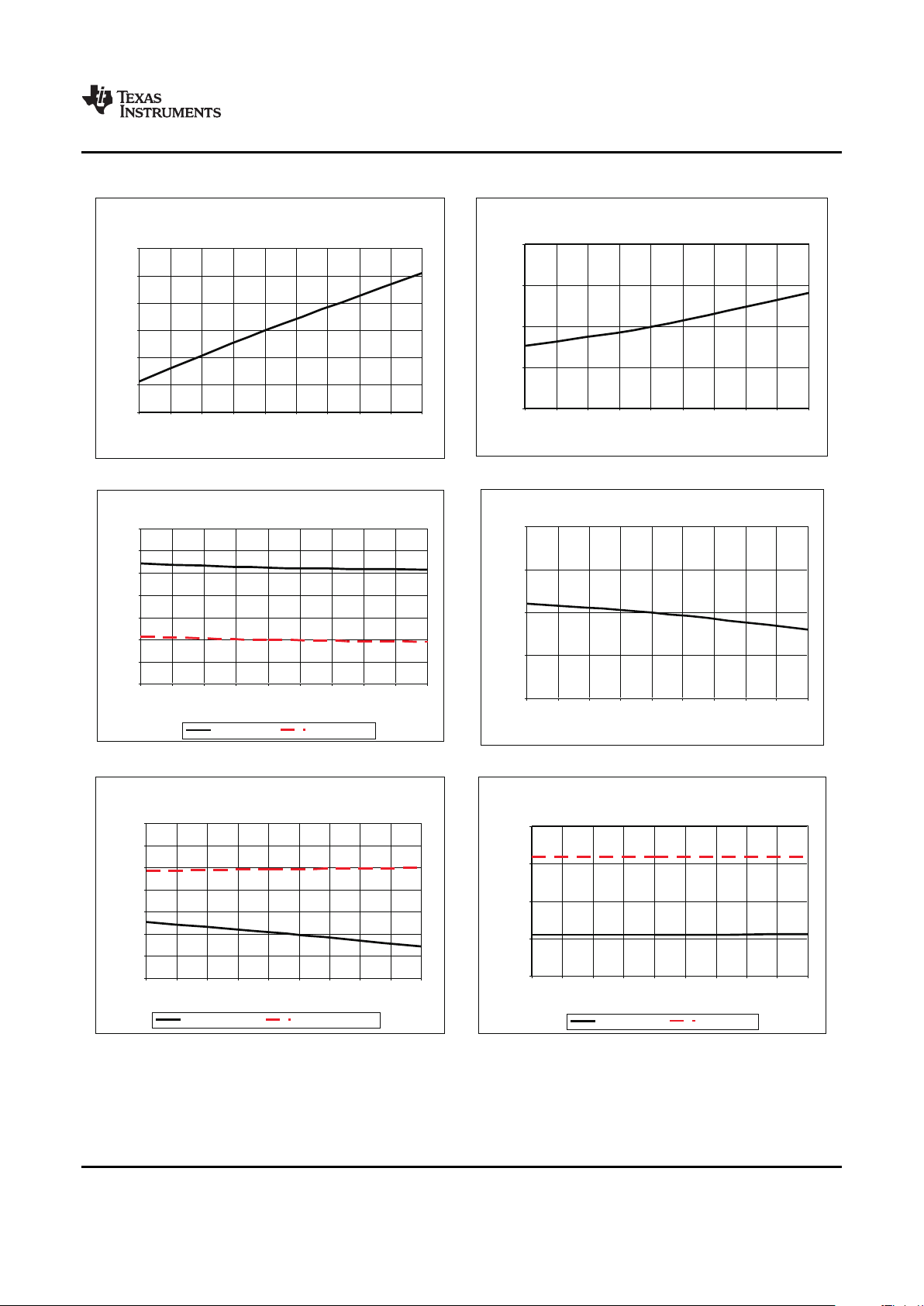
Figure 5. Figure 6.
Figure 7. Figure 8.
Figure 9. Figure 10.
Copyright © 2008, Texas Instruments Incorporated Submit Documentation Feedback 9
Product Folder Link(s): UCC28230 UCC28231
Page 10

Soft-Start Charge Current I
SS
over Temperature
24.80
24.85
24.90
24.95
25.00
25.05
25.10
25.15
25.20
-55 -35 -15 5 25 45 65 85 105 125
TJ-temperature, °C
Iss, µA
OffTimeMatching ∆T
OFF
overTemperature
1.00
1.50
2.00
2.50
3.00
3.50
4.00
-55 -35 -15 5 25 45 65 85 105 125
TJ-temperature,°C
∆T
OFF
,ns
UCC28230 Off Time T
OFF
and Dead Time T
DT
over Temperature
10
20
30
40
50
-55 -35 -15 5 25 45 65 85 105 125
TJ- te mperature, °C
T
OFF
, T
DT
, ns
Off Time
Dead Time
UCC28231 Off Time T
OFF
and Dead Time T
DT
over T emperature
10
20
30
40
50
-55 -35 -15 5 25 45 65 85 105 125
TJ- tempe rature, °C
T
OFF
, T
DT
, ns
Off Time
Dead Time
Maximum Off Time T
OFFMAX
at Low V
CS
over Temperature
170.00
180.00
190.00
200.00
210.00
220.00
-55 -35 -15 5 25 45 65 85 105 125
TJ- te mperatu re, °C
T
OFFM AX
, ns
Nominal Switching Frequency F
SWNOM
over Temperature
99.00
99.50
100.00
100.50
101.00
-55 -35 - 15 5 25 45 65 85 105 125
TJ- te mperature, ° C
F
SWNOM
, kHz
UCC28230
UCC28231
SLUS814A – FEBRUARY 2008 – REVISED JUNE 2008 ...................................................................................................................................................
www.ti.com
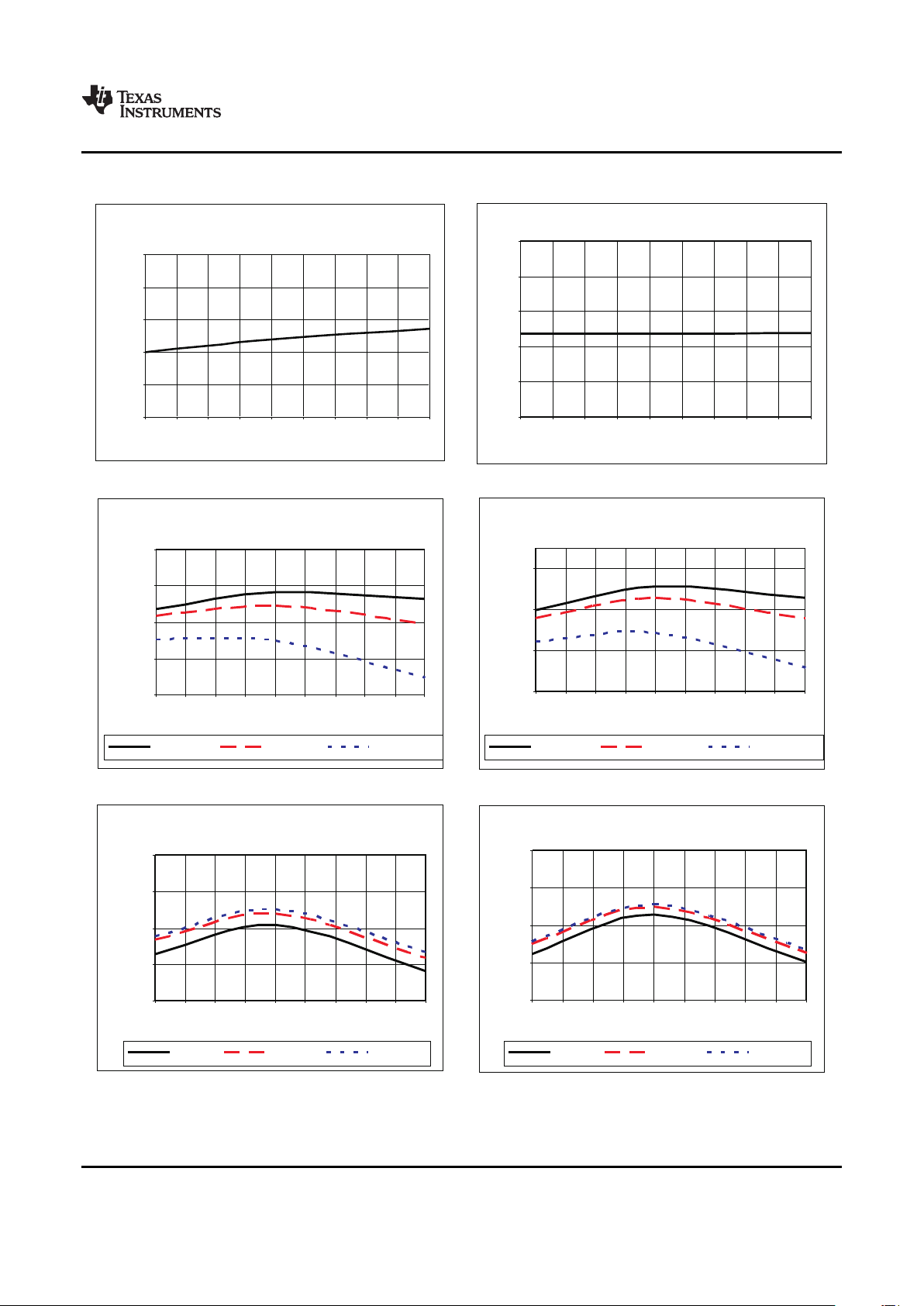
TYPICAL CHARACTERISTICS (continued)
Figure 11. Figure 12.
Figure 13. Figure 14.
Figure 15. Figure 16.
10 Submit Documentation Feedback Copyright © 2008, Texas Instruments Incorporated
Product Folder Link(s): UCC28230 UCC28231
Page 11
Maximum Switching Frequency F
SWMAX
over Temperature
500.00
510.00
520.00
530.00
540.00
550.00
-55 -35 - 15 5 25 45 65 85 105 125
TJ- temperature , °C
FSWMAX , kHz
Cycle-by-Cycle Current Limit Threshold
over Temperature
0.45
0.47
0.49
0.51
0.53
0.55
-55 -35 -15 5 25 45 65 85 105 125
TJ-tempera ture, °C
V
CS_LIM
, V
UCC28230 Refer ence Voltage at VDD=12V
over Te mperature and Load Curr ent
4.9 75
4.9 85
4.9 95
5.0 05
5.0 15
-55 -3 5 - 15 5 2 5 45 65 8 5 105 125
TJ- te mper ature, °C
V
REF
, V
Iload=10uA
Iload=1mA Iload=10mA
UCC28231 Refer ence Voltage at VDD=12V
over Te mperature and Load Curr ent
3.2 75
3.2 85
3.2 95
3.3 05
-55 -35 - 15 5 2 5 45 65 85 105 1 25
T
J
- te mper ature, °C
V
REF
, V
Iload=10uA
Iload=1mA Iload=10mA
UCC28230 Refer ence Voltage at I
LOAD
=1mA
over Te mper ature and Supply Voltage V
DD
4.990
4.994
4.998
5.002
5.006
-55 - 35 -15 5 25 45 65 85 105 125
TJ- te mper ature, °C
V
REF
, V
Vdd=7V
Vdd=12V Vdd=17V
UCC28231 Refer ence Voltage at I
LOAD
=1mA
over Te mperature and Supply Voltage V
DD
3.2 90
3.2 94
3.2 98
3.3 02
3.3 06
-55 -35 -1 5 5 25 45 65 8 5 105 1 25
TJ- te mper ature, °C
V
REF
, V
Vdd=7V
Vdd=12V Vdd=17V
UCC28230
UCC28231
www.ti.com
................................................................................................................................................... SLUS814A – FEBRUARY 2008 – REVISED JUNE 2008
TYPICAL CHARACTERISTICS (continued)
Figure 17. Figure 18.
Figure 19. Figure 20.
Figure 21. Figure 22.
Copyright © 2008, Texas Instruments Incorporated Submit Documentation Feedback 11
Product Folder Link(s): UCC28230 UCC28231
Page 12
Current Sense Propogation Delay T
CS
over Temperature
90.00
95.00
100.00
105.00
110.00
115.00
-55 -35 - 15 5 25 45 65 85 105 125
TJ- te mperatu re, °C
T
CS
, ns
Output Source Resistance R
SRC
and Sink Resistance
R
SINK
over Temperature
10.0
15.0
20.0
25.0
30.0
-55 -35 -15 5 25 45 65 85 105 125
TJ- te mperatur e, °C
R
SCR
, R
SINK
, O
Source Resistance
Sink Resist ance
UCC28230
UCC28231
SLUS814A – FEBRUARY 2008 – REVISED JUNE 2008 ...................................................................................................................................................
www.ti.com
TYPICAL CHARACTERISTICS (continued)
Figure 23. Figure 24.
Figure 25. O1_D and O2_D Duty Cycle Matching at V
CS
= Figure 26. O1_D and O2_D Duty cycle Matching at V
CS
=
0.14 V and V
OST
= 1 V 0.0 V and V
OST
= 1 V
12 Submit Documentation Feedback Copyright © 2008, Texas Instruments Incorporated
Product Folder Link(s): UCC28230 UCC28231
Page 13
UCC28230
UCC28231
www.ti.com
................................................................................................................................................... SLUS814A – FEBRUARY 2008 – REVISED JUNE 2008
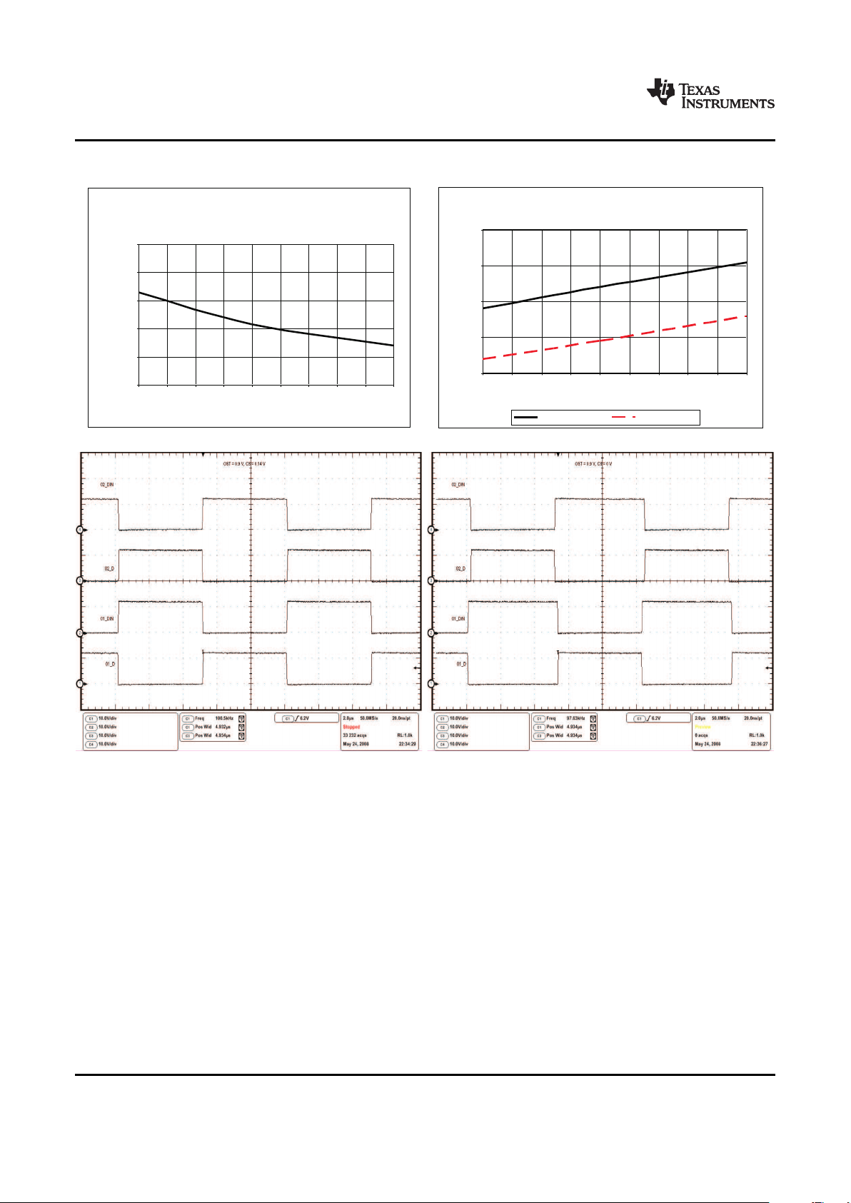
TYPICAL CHARACTERISTICS (continued)
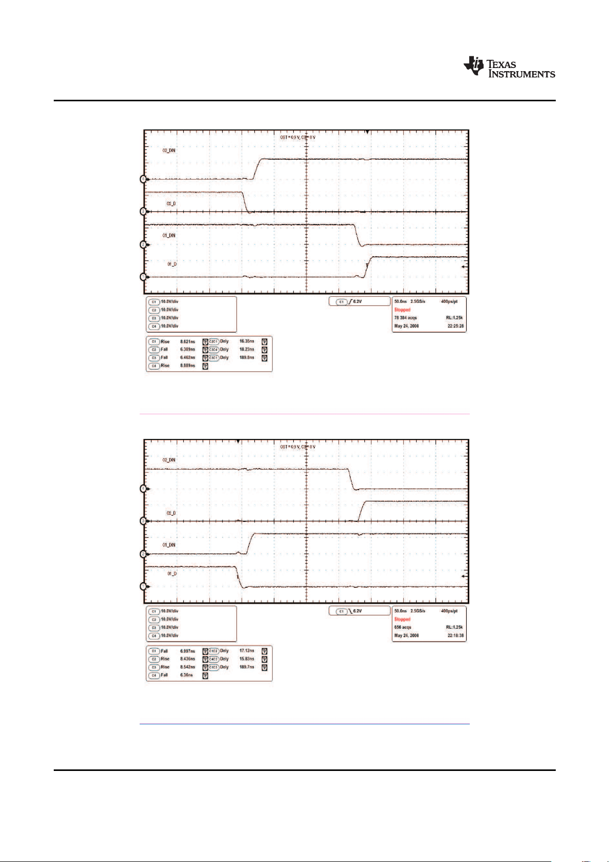
Figure 27. Output Waveforms During First Half Switching Cycle at V
CS
= 0.14 V and V
OST
= 1 V
Figure 28. Output Waveforms During Second Half Switching Cycle at V
CS
= 0.14 V and V
OST
= 1 V
Copyright © 2008, Texas Instruments Incorporated Submit Documentation Feedback 13
Product Folder Link(s): UCC28230 UCC28231
Page 14
UCC28230
UCC28231
SLUS814A – FEBRUARY 2008 – REVISED JUNE 2008 ...................................................................................................................................................
www.ti.com
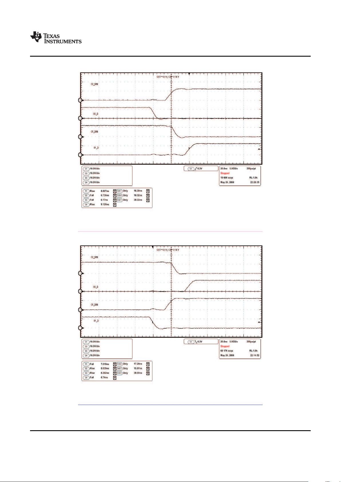
TYPICAL CHARACTERISTICS (continued)
Figure 29. Output Waveforms During First Half Switching Cycle at V
CS
= 0 V and V
OST
= 1 V
Figure 30. Output Waveforms During Second Half Switching Cycle at V
CS
= 0 V and V
OST
= 1 V
14 Submit Documentation Feedback Copyright © 2008, Texas Instruments Incorporated
Product Folder Link(s): UCC28230 UCC28231
Page 15

DETAILED DESCRIPTION
Start-Up Protection Logic
Internal Oscillator and Converter Switching Frequency
1
1 2
2500 2 4
=
+ ´
´ -
SW (nom)
OFF
IN
F
RT
. T
(V . )
(1)
UCC28230
UCC28231
www.ti.com
................................................................................................................................................... SLUS814A – FEBRUARY 2008 – REVISED JUNE 2008
Before the controller allows the start up, the following conditions must be met:
• VDD voltage exceeds rising UVLO threshold 6.3 V typical
• The reference voltage 5 V for UCC28230 or 3.3 V for UCC28231 is available
• Junction temperature is below the thermal shutdown threshold 130 ° C min
• The voltage at soft-start capacitor is not below 0.55 V typical
If all those conditions are met, an internal enable signal EN is generated that initiates the soft start process. The
duty cycle during the soft start is defined by the voltage at the SS pin or by cycle-by-cycle current limit circuit
depending on load conditions.
The oscillator frequency is set by an external resistor at RT pin (see Figure 3 and Figure 4 ). The oscillator
frequency F
OSC
is twice that of converter switching frequency F
SW
. The oscillator performs the following main
functions:
• Generates clock signal CLK to synchronize internal functional blocks
• By changing the switching frequency during the start up and cycle-by-cycle current limit, the oscillator limits
the current ripple at the output inductor allowing the use of small output inductor and start with large output
capacitor
Oscillator can operate in the following modes:
• Fixed volt-second mode of operation when the resistor RT is connected between V
IN
and RT pin. In this mode
the switching frequency increases in accordance to an input voltage rise
• Fixed switching frequency mode when the resistor RT is connected between VREF and RT pins.
The switching frequency of converter is defined as F
SW(nom)
= 1/T
SW(nom)
(see Figure 33 ). Equation 1 is used to
calculate the nominal switching frequency of the converter and its transformer.
Where RT is in k Ω , V
IN
is in volts, T
OFF
is in ms and F
SW(nom)
is in kHz.
Copyright © 2008, Texas Instruments Incorporated Submit Documentation Feedback 15
Product Folder Link(s): UCC28230 UCC28231
Page 16

2 4
2500
-
= ´
IN
SW (nom)
(V . )
F
RT
(2)
0
100
200
300
400
500
600
700
800
900
1,000
100 300 500 700 900 1100
RT Res istance ( kO)
Switching F requency (k Hz)
Vin=36V
Vin=48V
Vin=60V
0
100
200
300
400
500
600
700
800
36 40 44 48 52 56 60
Vin V oltage (V)
Switching F requency (kHz )
RT=200kohm
RT=400kohm RT=1,100kohm
2 4
2500
SW (nom)
(VREF . )
F
RT
-
= ´
(3)
UCC28230
UCC28231
SLUS814A – FEBRUARY 2008 – REVISED JUNE 2008 ...................................................................................................................................................
www.ti.com
In most applications, T
OFF
is set at about 40~50 ns, which can be neglected compared to the total oscillator
period. Therefore Equation 1 can be simplified as:
In this equation RT is in k Ω , V
IN
is in volts and F
SW(nom)
is in kHz.
Figure 31 shows how the nominal switching frequency of converter depends on value of resistor RT, and
Figure 32 shows how the switching frequency changes over the input voltage range in case of fixed volt-second
mode of operation. The T
OFF
is set to 40 ns for both figures.
Figure 31. Nominal Switching Frequency of Converter vs Figure 32. Switching Frequency Variation Over the Input
Resistor RT Voltage for Fixed Volt-Second Mode of Operation
Fixed frequency mode of operation can be achieved by connecting the resistor RT between VREF and RT pins.
In such case the switching frequency is defined by the following Equation 3 , where the impact of T
OFF
is
neglected as well.
In this equation the RT is in k Ω , VREF is in volts and F
SW(nom)
is in kHz.
16 Submit Documentation Feedback Copyright © 2008, Texas Instruments Incorporated
Product Folder Link(s): UCC28230 UCC28231
Page 17

Output Signals
O1_D
O2_D
O2_DIN
O1_DIN
T
DT
T
DT
T
DT
T
DT
T
OFF
T
OFF
T
OFF
T
OFF
T
CLAMP
T
CLAMP
T
CLAMP
T
CLAMP
T
SWNOM
T
OUT_D
UCC28230
UCC28231
www.ti.com
................................................................................................................................................... SLUS814A – FEBRUARY 2008 – REVISED JUNE 2008
The UCC28230/1 has two push-pull outputs O1_D and O2_D that provide D pulse signals to external drivers.
The additional two outputs O1_DIN and O2_DIN provide 1-D output pulses with dead time between D and 1-D
pulses to avoid shoot-through currents. Such combination of outputs allows use of UCC28230/1 either with
self-driven synchronous rectifier, or with the control-driven synchronous rectifier in push-pull, half-bridge or
full-bridge configuration.
For the full-bridge self-driven rectifier configuration, outputs O1_D and O2_D control high-side MOSFETs while
outputs O1_DIN and O2_DIN control low-side MOSFETs thus shorting the primary winding during (1-D)
switching cycle. This avoids number of issues related to self-driven rectification such as start up disabling,
reverse current during parallel operation, tendency to oscillate during low duty cycles. The applications circuit for
this configuration is shown on Figure 1 and the output signal timing diagrams are shown in Figure 33 .
Figure 33. D and (1-D) Output Pulses Providing Dead Time T
DT
in Each Leg and the Off Time T
OFF
Between Upper FETs That Includes Some Overlapping Time T
CLAMP
.
In the steady state condition an unregulated bus converter operates at maximum duty cycle thus having
minimum overlapping T
CLAMP
of (1-D) outputs. During start up or cycle-by-cycle current limit, the duty cycle can
be very low, so (1-D) output pulses occupy most of the switching cycle time. This provides zero voltage clamping
of the transformer ’ s primary winding. The UCC28230/1 also includes an off-time control feature. This feature
allows user to increase off time T
OFF
when the converter output current is below a programmable current
threshold. This feature reduces switching losses of the synchronous rectifier at light load and it is described in
detail in Offtime Control Circuit section.
For the control driven half-bridge topology, the outputs O1_D and O2_D provide control pulses for the high-side
and low-side MOSFETs, while the outputs O1_DIN and O2_DIN can be used to drive the pulse transformers
providing control signals to the secondary-side MOSFET rectifiers as shown in Figure 2 .
In case of full-bridge topology with the control-driven rectifier, the outputs O1_DIN and O2_DIN are used to
control primary low-side MOSFETs as well as the secondary-side rectifier MOSFETs.
Copyright © 2008, Texas Instruments Incorporated Submit Documentation Feedback 17
Product Folder Link(s): UCC28230 UCC28231
Page 18

Start-Up Frequency Control Circuit
=
+
OUT
OUT OFF
T _ D
D
T _ D T
(4)
Fsw vs DutyCycle, RT=1M tied to Vin,
Vost=1V, R3(OS)=15k, Toff=53ns, Vcs=0.4V
0
100
200
300
400
500
600
700
800
900
0 10 20 30 40 50 60 70 80 90 100
Duty Cycle, %
Fsw, kHz
Vin=48V
Vin=36V Vin=72V Vin=48V, RT=287K
FswvsDutyCycle,RT=1MtiedtoVin,
Vost=1V,R3(OS)=15k,Toff=196ns,Vcs=0V
0
100
200
300
400
500
600
700
800
900
0 10 20 30 40 50 60 70 80 90 100
DutyCycle,%
Fsw
,
Vin=48V Vin=36V Vin=72V Vin=48V,RT=287K
UCC28230
UCC28231
SLUS814A – FEBRUARY 2008 – REVISED JUNE 2008 ...................................................................................................................................................
www.ti.com
The start-up frequency control circuit addresses the need for bus converter to start at heavy load with a large
output capacitance. In the steady state condition bus converters operate with the minimum off time and as the
result, the output inductor current ripple is low. Therefore the output inductor value is able to be selected very low
to save the size and cost. During over current or soft start condition the duty cycle is controlled by the
cycle-by-cycle current limit circuit or by the voltage at soft-start capacitor. In this condition, the duty cycle D for
the output inductor can be anywhere between 0 and 1 causing significant output inductor current ripple that
reaches its maximum at duty cycle D = 0.5. The current limit circuit on primary side limits the peak current, not
the average current. The limiting of peak current with a large ripple causes the fold back characteristic of
converter output, which prevents the converter from ever reaching its nominal steady state output voltage.
The output inductor duty cycle is a ratio of output pulses T
OUT
_D at pins O1_D and O2_D to the half of switching
cycle T
SW(nom)
, i.e. T
OUT
_D +T
OFF
(see Figure 33 ):
The start-up frequency control circuit changes the switching frequency during the start up or during the
cycle-by-cycle current limit to maintain the output inductor current ripple almost constant at any duty cycle D. This
allows an additional cost and size saving because the output inductor can be selected based on steady state
condition rather than the transient condition, which dictates significantly larger inductance value and size.
Examples of switching frequency changes over duty cycle variation for the selected nominal frequencies 100 kHz
and 450 kHz are shown in Figure 34 . The plots are given for the nominal off time at 53 ns and 77 ns (right
column) and for no load off time at 196 ns, 209 ns accordingly. It is shown that the impact of nominal off time on
switching frequency is minimal. However the no load off time causes visible frequency reduction especially at
maximum frequency when the duty cycle D is around 0.5.
Switching Frequency Plots vs Duty Cycle for F
SW(nom)
Set at 100 kHz and 450 kHz at Different No Load and
Nominal T
OFF
Time Sets.
Figure 34. Figure 35.
18 Submit Documentation Feedback Copyright © 2008, Texas Instruments Incorporated
Product Folder Link(s): UCC28230 UCC28231
Page 19

Fsw vs DutyCycle at Lout, RT=1M tie d to Vin,
Vost=1V, R3(OS)=30k, Toff=209ns, Vcs=0V
0
100
200
300
400
500
600
700
800
900
0 10 20 30 40 50 60 70 80 90 100
Duty Cycle, %
Fsw, kHz
Vin=48V
Vin=36V Vin=72V Vin= 48V, RT=287K
Fsw vs Duty Cycle, RT=1M tied to Vin,
Vost=1V, R3(OS)=30k, Toff=77ns, Vcs=0.4V
0
100
200
300
400
500
600
700
800
900
0 10 20 30 40 50 60 70 80 90 100
Duty Cycle, %
Fsw, kHz
Vin=48V
Vin=36V Vin=72V Vin=48V, RT=287K
375@ +
SW (m ax) SW (nom)
F F kHz
(5)
0 1 0 9
0 4 0 6
1 0 1 0 4 0 6 0 9
ì
< >
ï
» £ £
í
ï
´ ´ - £ < < £
î
SW (nom)
SW SW (max)
SW (max)
F D . or D .
F F . D .
F D ( D ) . D . or . D .
(6)
1
4 1
´ ´ -
=
´ ´ ´ - ´
IN
O
TR SW (max) O
V D ( D)
L
N F ( KL ) I
(7)
2
L (ma x) L ( ch )
I I£ ´
(8)
UCC28230
UCC28231
www.ti.com
................................................................................................................................................... SLUS814A – FEBRUARY 2008 – REVISED JUNE 2008
Figure 36. Figure 37.
To avoid jittering during the fast duty cycle change and reduce sensitivity to noise, the transfer function of
switching frequency of the converter to the duty cycle has 20-kHz bandwidth well below the switching frequency.
The maximum switching frequency F
SW(max)
of converter is given by:
Where T
OFF
affect is neglected as well and the frequency is in kHz. T
OFF
has more affect on switching frequency
F
SW
at very high frequency. One can see how T
OFF
affects FSW(max) in Figure 34 .
The relation between switching frequency F
SW
and duty cycle D in Figure 34 can be best described by:
Knowing the maximum switching frequency F
SW(max)
at D = 0.5 and the ratio of peak output inductor current to
the nominal load current KL = I
L(max)
/IO, allows calculate the output inductor value by using the following
Equation 7 .
In this equation N
TR
is transformer turns ratio from primary winding to the secondary. The selection of KL
depends on the average output inductor current I
L(ch)
that needs to be provided during the start up to charge the
output capacitor and supply the load. To ensure that the converter starts the following condition needs to be met.
How I
L(ch)
needs to be defined is described in the following section.
Copyright © 2008, Texas Instruments Incorporated Submit Documentation Feedback 19
Product Folder Link(s): UCC28230 UCC28231
Page 20

Soft Start
25
2 85 0 85
m´
=
-
SS
SS
T A
C
( . V . V )
(9)
0 85
25 m
´
=
SS
DEL
C . V
T
A
(10)
UCC28230
UCC28231
SLUS814A – FEBRUARY 2008 – REVISED JUNE 2008 ...................................................................................................................................................
www.ti.com
The soft-start pin SS is multi-function pin used for the following operations:
• Soft start with the duty cycle graduate increase from zero to its maximum value of almost 100%
• Setting cycle-by-cycle over current hiccup mode conditions
• On/off control for the converter
• Indicator of severe short circuit condition
The soft-start duration is defined by an external capacitor connected between SS pin and ground and the internal
charge current that has typical value of 25 µ A. During soft start, the duty cycle of controller is determined by the
voltage at SS pin. Below the 0.85-V threshold, there are no switching pulses at the outputs. Pulling the soft-start
pin externally below or above 0.55-V typical threshold can be used for the on/off control. When the soft-start
voltage is rising from 0.85 V up to 2.85 V and there is no current limit condition, the duty cycle applied to the
output inductor is increasing accordingly from 0 to 1. The external capacitor C
SS
value can be defined by the
Equation 9 :
For example, if the soft-start time T
SS
is selected 10 ms, then the soft-start capacitor C
SS
is equal to 125 nF and
the closest available standard value100 nF can be selected. Notice, that the output pulses do not appear until the
voltage at soft start capacitor reaches 0.85 V. An additional typical soft start delay caused by this can be
calculated by the Equation 10 :
For the C
SS
= 100 nF the calculated delay is 3.4 ms.
20 Submit Documentation Feedback Copyright © 2008, Texas Instruments Incorporated
Product Folder Link(s): UCC28230 UCC28231
Page 21

1
4 4
TR IN IN
OUT O(lim)
m SW TR O SW
N V D V D ( D)
I I
L F N L F
´ ´ ´ ´ -
= - -
´ ´ ´ ´ ´
(11)
- ´ ´
= - ´
IN OUT PR TR
O OUT SEC
TR
(V I R / N ) D
V I R
N
(12)
0.1 1 10
0.01
0.1
1
10
100
1.10
3
Cout=100uF
Cout=1000uF
Cout=10000uF
Soft start time, ms
Required primary current, A
UCC28230
UCC28231
www.ti.com
................................................................................................................................................... SLUS814A – FEBRUARY 2008 – REVISED JUNE 2008
The Equation 9 and Equation 10 use typical values for calculations. If the output capacitor of the bus converter is
large and the soft-start time is selected relatively short, then the converter should deliver large charge current to
the output capacitor to provide the required soft start time. This current might hit the current limit threshold and
the soft-start time can be longer than expected. Figure 38 provides an estimation of the required average charge
current from the converter to charge the output capacitor within predetermined soft-start time. To avoid tripping of
the current limit comparator, the current limit threshold should be set above the required average charge current
with the additional current required by the load, half of the output inductor current ripple and the magnetizing
current of the transformer. The average output inductor charge current I
OUT
during the cycle-by-cycle current limit
can be described by the following equation:
Here I
O(lim)
is the output current limit and L
m
is magnetizing inductance. The I
O(lim)
is always less or equal to I
L(max)
to avoid saturation of the output inductor. The output voltage V
O
over output current I
OUT
is as follows
Where R
PR
is the equivalent resistance on primary side and R
SEC
is the equivalent resistance on secondary side.
Figure 38. Estimated Average Primary-Side Charge Current From the Converter Required to Charge the
Output Capacitor of Specified Value Within Required Soft-Start Time
Copyright © 2008, Texas Instruments Incorporated Submit Documentation Feedback 21
Product Folder Link(s): UCC28230 UCC28231
Page 22

0 5 10 15 20 25 30 35 40 45 50 55 60 65 70 75 80
0
2
4
6
8
10
12
100kHz
200kHz
400kHz
Vout Steady State (top)
Cycle-by-cycle current limit
Iout, A
Vout, V
UCC28230
UCC28231
SLUS814A – FEBRUARY 2008 – REVISED JUNE 2008 ...................................................................................................................................................
www.ti.com
Figure 39 shows the output voltage as function of the average load current limited by the cycle-by-cycle current
limit threshold after substituting (9) into (10). These plots are generated for the following conditions: V
IN
= 48 V,
N
TR
= 5, LO= 0.1 µ H, L
m
= 75 µ H, I
O(lim)
= 73 A, R
pr
= 25 m Ω and R
SEC
= 4 m Ω at F
SW
= 100 kHz, 200 kHz and
400 kHz. This fold back type of behavior limits the start-up capability of unregulated IBC. One can see that at
100-kHz switching frequency and 0.5 duty cycle (i.e., V
O
≈ 5 V), only about 11.5 A average current is available to
charge the output capacitor while at 400 kHz, the charge current can be as high as 60 A. The plots in Figure 39
show the required average charge current reflected to the primary side of the converter with N
TR
= 5:1 for
different output capacitor values depending on the selected soft-start time, which do not count extra current
drawn by the load itself. Therefore the significant output inductor current ripple not only can trip the peak current
mode control current limit circuit to reduce the average output inductor current available to charge the output
capacitor, but also can cause the hiccup or latch off of the converter to prevent it from starting at all. Increasing
the current limit threshold to allow the normal start up of the converter can cause potential overstress if for some
reason the load exceeds its nominal current during the steady state operation.
Without frequency control circuit, the module operates only at 100 kHz. At 100 kHz the secondary charge current
available is only 11.5 A, which is only 2.3 A if reflected to the primary side (N
TR
= 5). The 2.3-A current is able to
charge the 10000- µ F output capacitor within 10 ms provided that there is no additional load current applied.
Figure 39. Output Voltage at Cycle-by-Cycle Current Limit
22 Submit Documentation Feedback Copyright © 2008, Texas Instruments Incorporated
Product Folder Link(s): UCC28230 UCC28231
Page 23

Current Sensing
UCC28230
UCC28231
www.ti.com
................................................................................................................................................... SLUS814A – FEBRUARY 2008 – REVISED JUNE 2008
With the frequency control circuit, the start up switching frequency is 400 kHz. At 400-kHz, 60-A charge current is
available, which is 12 A if reflected to the primary side. Assuming as in previous case 2.3 A portion of this current
is used to charge the 10000- µ F output capacitor within 10 ms, the remaining 9.7 A on primary side allows extra
48.5-A current to supply the load itself on the secondary side. Figure 40 shows a design example using the
startup frequency control of UCC28230 to start up with 30-A constant load current and 10900- µ F output
capacitor.
Using SS pin and soft-start capacitor to set cycle-by-cycle over-current hiccup mode is described further in
Cycle-by-Cycle Current Limit section and Short Circuit Protection section.
Figure 40. Start up at 30-A Constant Current Load With C
O
= 10900 µ F
The current sensing pin CS is used for the following functional blocks:
• Cycle-by-cycle current limit
• Adjustable off-time control
• Short circuit protection
Copyright © 2008, Texas Instruments Incorporated Submit Documentation Feedback 23
Product Folder Link(s): UCC28230 UCC28231
Page 24

Cycle-by-Cycle Current Limit and Short Circuit Protection
( )
( )
25 1 5 m= - ´ - +
DS
I D A
(13)
Soft-Start
Normal
Operation
Cycle-by-
CycleIlim.
Off Timebeforerestart Soft-
Restart
0
SSpin,
Volts
Ids=(-25x(1-D)+5)μA
Ihcc=-2.5μA
OutputPulses, D
25μA
FastPullUp
by
1kΩ Switch
SSClampVoltage 4.5
Outp. Enbl. Thresh. 0.85
SSShDn. Thresh. 0.55
PullUp Thresh. 3.5
Dmax Thresh. 2.85
(forreference)
Iss=25μA
t
( )
4 5 3 5
20 m
´ -
=
SS
CL( on)
C . V . V
T
A
(14)
( )
3 5 0 55
2 5 m
´ -
=
SS
CL( off )
C . V . V
T
. A
(15)
UCC28230
UCC28231
SLUS814A – FEBRUARY 2008 – REVISED JUNE 2008 ...................................................................................................................................................
www.ti.com
The cycle-by-cycle current limit provides peak current limit on primary side when the load current exceeds its
predetermined threshold. For peak current mode control, certain leading edge blanking time is needed to prevent
the controller from false tripping due to switching noise. In order to save external RC filter for the blanking time,
an internal 50-ns filter at CS input is provided. With the 50-ns delay from the input of the current sense
comparator to the outputs, the total propagation delay T
CS
from CS pin to outputs is about 100 ns. An external
RC filter is still needed if the power stage requires more blanking time. The 0.5-V ± 3% cycle-by-cycle current limit
threshold is optimized for efficient current transformer based sensing. The duration when a converter operates at
cycle-by-cycle current limit depends on the value of soft-start capacitor and how severe is the over current
condition. The soft-start capacitor value also determines the so called hiccup mode off-time duration. These are
achieved by the internal discharge current IDS(Equation 13 ) and I
HCC
(see Figure 41 ) at SS pin.
When the output inductor duty cycle D at cycle-by-cycle current limit is above 80%, the converter operates as the
current source and does not enter into hiccup mode at all. This allows parallel operation of converters using
droop current sharing technique. At more severe over current condition, the duty cycle D becomes lower and Ids
becomes large enough to initiate hiccup mode with periodical restart. The behaviour of the converter at different
modes and related soft-start capacitor charge/discharge currents are shown in Figure 41 .
Figure 41. Timing Diagram of Soft-Start Voltage V
SS
at Different Modes of Operation Defined by Voltage
Thresholds and Related Soft-Start Capacitor Charge/Discharge Currents
The largest discharge current is at the duty cycle close to zero as 20 µ A. This current sets the shortest operation
time during the cycle-by-cycle current limit which is defined as:
Thus, if the soft-start capacitor CSS = 100 nF is selected, then the T
CL(on)
time will be 5 ms.
To calculate the hiccup off time T
CL(off)
before the restart, Equation 15 needs to be used:
24 Submit Documentation Feedback Copyright © 2008, Texas Instruments Incorporated
Product Folder Link(s): UCC28230 UCC28231
Page 25

UCC28230
UCC28231
www.ti.com
................................................................................................................................................... SLUS814A – FEBRUARY 2008 – REVISED JUNE 2008
With the same soft-start capacitor value 100 nF, the off time before the restart is going to be 118 ms. Notice, that
if the over current condition happens before the soft-start capacitor voltage reaches the 3.5-V threshold during
start up, the controller limits the current but the soft-start capacitor continues to be charged. As soon as the 3.5-V
threshold is reached, the soft-start voltage is quickly pulled up to the 4.5-V threshold by an internal 1-k Ω R
DS(on)
switch and the cycle-by-cycle current limit duration timing starts by discharging the soft-start capacitor.
Depending on specific design requirements, the user can override default parameters by applying external
charge or discharge currents to the soft-start capacitor. Figure 42 shows the operation of a full-bridge system at
cycle-by-cycle current limit. The waveforms include drain-source voltages of synchronous rectifiers and voltage at
CS pin. The whole cycle-by-cycle current limit and hiccup operation is shown in Figure 43 . In this example the
cycle-by-cycle current limit lasts about 25 ms followed by 150 ms of off time.
Figure 42. Cycle-by-Cycle Current Limit
Figure 43. Hiccup Mode with Cycle-by-Cycle Current Limit at I
OUT
= 60 A
Copyright © 2008, Texas Instruments Incorporated Submit Documentation Feedback 25
Product Folder Link(s): UCC28230 UCC28231
Page 26

SoftStart
Thesecondcurrentlimitthreshold0.7V
ishitatCSpinindicatingshortcircuit
Off Timebeforerestart
Soft-
Restart
0
SSpin,
Volts
4.5
Iss=25µA
Ihcc= -2.5µA
SSClampVoltage
OutputPulses, D
FastPullUpby
1kΩ Switch
Outp. Enbl. Thresh. 0.85
SSShDn. Thresh. 0.55
( )
4 5 0 55
2 5 m
´ -
=
SS
CL( off )
C . V . V
T
. A
(16)
UCC28230
UCC28231
SLUS814A – FEBRUARY 2008 – REVISED JUNE 2008 ...................................................................................................................................................
www.ti.com
In the event of a severe short circuit condition, the current sense voltage will exceed the short circuit threshold
set at 0.7 V min. At this point the controller shuts down the converter with propagation time 100 ns and pulls the
soft start pin up to the 4.5-V threshold. (see Figure 44 ).
Figure 44. Timing Diagram for the Soft-Start Capacitor Voltage V
SS
During Short Circuit Protection
At this condition the soft-start voltage is forcibly pulled up even if the soft-start charge is not completed. After
that, the soft-start capacitor is discharged by 2.5- µ A current until its voltage reaches the 0.55 V in order to
resume the soft-start cycle again. The duration of off time before the restart is defined by Equation 16 :
With the same soft-start capacitor value 100 nF, the off time before the restart is going to be about 158 ms.
Similar to the over current condition, the hiccup mode with the restart can be override by user if a pull-up resistor
is connected between the SS and VREF pins. If the pull-up current provided by the resistor exceeds 2.5 µ A, then
the controller remains in the latch-off mode. In this case, an external soft-start capacitor value should be
calculated with the additional pull-up current taken into account. The latch-off mode can be reset externally if the
soft-start capacitor forcibly discharged below 0.55 V or the V
DD
voltage is lowered below the UVLO threshold.
26 Submit Documentation Feedback Copyright © 2008, Texas Instruments Incorporated
Product Folder Link(s): UCC28230 UCC28231
Page 27

Off-Time Control Circuit
Off TimeControl Threshold
(SetbyresisterdividerR1/R2from
PinVREFtopinOST andtoGND)
0 Iout
T
OFF
T
CLAMP
T
DT
T
DT
T
CLAMP
Ensures
nocross
conductionat
lightload
Provides
minimumdiode
conductionover
widerangeof
loadconditions
T
DT
Hysteresis=I
HYST
xR1xR2/(R1+R2)
T
OFFMAX
atlightload=5x T
OFF
with Off TimeControl
Thresholdsetto20%ofI
MAX
T
OFF
≈2.5×TDTatheavyload
(setbyresisterR3from
pinOStoGND)
´ ´
= ´
´
CS CT ( pr ) PT (sec)
CS OUT
PT ( pr ) C T (sec)
R W W
V I
W W
(17)
UCC28230
UCC28231
www.ti.com
................................................................................................................................................... SLUS814A – FEBRUARY 2008 – REVISED JUNE 2008
The off time control circuit provides optimal off time between O1_D and O2_D outputs depending on the load
current condition. The UCC28230/1 implements the off time control approach based on step function with
hysteresis (see Figure 45 ).
Off-time control is an important feature to address an optimal operation of self-driven synchronous rectifier over
the whole load current range. In self-driven rectifier applications, the turn-on and off time of the synchronous
FETs is defined by the current of output inductor and its polarity. Some additional energy is also provided from
the magnetizing inductance of a power transformer but it may not be sufficient for the fast switching. Therefore,
at light load the off-time should be longer than at full load to allow previously conducting rectifier MOSFET to be
completely turned off before the next switching half-cycle. This ensures the rectifier MOSFET having enough
time to turn off before the primary-side MOSFET forces it to turn off. The turn off of the rectifier MOSFET, while
still conducting, results in a current surge followed by a significant voltage spike which lowers the efficiency and
reliability of converter.
Figure 45. The Off Time Change as Function of Load Current
Usually there is no direct access to the load current of bus converters, so the primary current sensing is used to
replicate load current changes (see Figure 45 ). The largest part of the primary current is the load current on
secondary side of power transformer reflected into the primary side in accordance to transformer ’ s turn ratio. The
primary current includes not only the reflected load current, but also magnetizing current. However, for the most
practical applications the accuracy of solution with magnetizing current included is sufficient because in this
application the magnetizing current is only small percentage of overall current. With this assumption, the voltage
at pin CS can be defined as:
Copyright © 2008, Texas Instruments Incorporated Submit Documentation Feedback 27
Product Folder Link(s): UCC28230 UCC28231
Page 28

UCC28230 Off Time T
OFF
and Dead Time TDvs R
OS
0
10
20
30
40
50
60
70
80
90
100
0 5 10 15 20 25 30 35
R
OS
(kΩ)
T
OFF
and T
D
(ns)
Off Time
Dead Time
UCC28230 Off Time T
OFF
and Dead Time TDvs R
OS
0
50
100
150
200
250
300
350
0 15 30 45 60 75 90 105 120 135 150
ROS(kΩ)
T
OFF
and T
D
(ns)
Off Time
Dead Time
UCC28231 Off Time T
OFF
and Dead Time TDvs R
OS
0
50
100
150
200
250
300
0 20 40 6 0 8 0 100 12 0 140 160 180 200
R
OS
(kΩ)
T
OFF
and T
D
(ns)
Off Time
Dead Time
UCC28231 Off Time T
OFF
and Dead Time TDvs R
OS
0
10
20
30
40
50
60
70
80
90
100
0 5 10 1 5 20 25 30 35 4 0 45 50 55 60
ROS(kΩ)
T
OFF
and T
D
(ns)
Off Time
Dead Time
UCC28230
UCC28231
SLUS814A – FEBRUARY 2008 – REVISED JUNE 2008 ...................................................................................................................................................
www.ti.com
Where I
OUT
is the output inductor current, R
CS
is the current sense resistor, W
PT(pr)
and W
PT(sec)
are the primary
and secondary number of turns of power transformer windings and the W
CT(pr)
and W
CT(sec)
are the primary and
secondary number of turns of current transformer windings.
UCC28230/1 uses OS pin and OST pin to program the nominal off time T
OFF
and the output current threshold
where the off time steps up to the new value T
OFF(max)
. The dead time Tdand nominal off time T
OFF
are set by
resistor R3 between OS pin and GND (Figure 3 , Figure 4 and Figure 50 ). Figure 46 shows how to choose R3
resistance to achieve the dead time Td and nominal off time T
OFF
for both UCC28230 and UCC28231. For
example, if a 40ns nominal T
OFF
is needed, the resistor value should be 8.45k Ω , and Td is about 17ns for
UCC28230 and 15ns for UCC28231. 15 k Ω R3 at OS pin sets T
OFF
to 50 ns and Tdto 23 ns for UCC28230, with
T
OFF
as 47 ns and Tdas 19 ns for UCC28231. Based on Figure 46 , one can tell that T
OFF
is about 2.2 to 2.64
times of Tdfor UCC28230, and 2.25 to 2.75 times of Tdfor UCC28231.
Figure 25 through Figure 30 from Typical Waveforms show the output switching waveforms including rise and fall
time and off time T
OFF1
, T
OFF2
for each half switching cycle and dead time Td1, Td2, T
d3
and T
d4
for each half
switching cycle.
Off time and dead time selection based on the resistor R3 value.
Figure 46. Figure 47.
Figure 48. Figure 49.
28 Submit Documentation Feedback Copyright © 2008, Texas Instruments Incorporated
Product Folder Link(s): UCC28230 UCC28231
Page 29

2
1 2
= ´
+
R
VOST VREF
R R
(18)
VREF
CS
CT
OS
Is
R 1
R 2
1
2
6
T
OFF
set
circuit
3
OST
R 3
5VforUCC28230,
3.3VforUCC28231
To Logic Block
Iprim
X
10
filtering
I
HYST
= 10 µA
RCS
Cycle-by-Cycle
CurrentLimit
1 2
1 2
´
= ´
+
hyst hyst
R R
V I
R R
(19)
UCC28230
UCC28231
www.ti.com
................................................................................................................................................... SLUS814A – FEBRUARY 2008 – REVISED JUNE 2008
The next step is to set the output current threshold below that the off time changes to its maximum value. This
threshold is defined as:
The increase of off time at light load condition is provided by the increasing of overlapping time T
CLAMP
of
O1_DIN and O2_DIN outputs (see Figure 33 ). This ensures the faster turning off of the rectifier MOSFETs when
the primary winding is clamped. The dead time between the switching of primary MOSFETs in each leg remains
the same over the load current, which is still proportional to nominal off time as shown in Figure 46 .
Figure 50. The Off-Time Control Circuit Using Comparator With Hysteresis
Selecting optimal hysteresis is important to avoid oscillation. UCC28230/31 provides the flexibility of
programming the hysteresis with internal 10- µ A current I
HYST
and the values of external resistors R1 and R2 (see
Figure 50 ). Equation 19 shows how to choose the hysteresis.
In some cases, the disabling of off-time control circuit is needed, which can be done by simply connecting OST
pin to GND or to VREF. Connecting OST pin to the VREF is characterized in the electrical table and is the
preferable way to maintain fixed off time set by resistor R3.
The load dependent dead time will cause a slight change in output duty cycle at the programmed transition point
from light load to heavy load and vice-versa. This slight change in duty cycle corresponds to a slight change in
output voltage.
Copyright © 2008, Texas Instruments Incorporated Submit Documentation Feedback 29
Product Folder Link(s): UCC28230 UCC28231
Page 30

APPLICATION INFORMATION
DESIGN EXAMPLE
1
0
V
UCC28230
UCC28231
SLUS814A – FEBRUARY 2008 – REVISED JUNE 2008 ...................................................................................................................................................
www.ti.com
Two design examples are provided to show how to design an intermediate bus converter with UCC28230/1.
Design Example 1 provides a concise step-by-step design. Its design specifications, schematics and test results
are illustrated on efficiency, power dissipation and output voltage regulation. Design Example 2 is to show an
industry standard quarter brick module design with 12-layer boards and embedded magnetic parts. Its design
specifications, schematics, and test results are provided.
Figure 51. Design Example of IBC Using UCC28230 Controller Device
30 Submit Documentation Feedback Copyright © 2008, Texas Instruments Incorporated
Product Folder Link(s): UCC28230 UCC28231
Page 31

Design Goals
UCC28230
UCC28231
www.ti.com
................................................................................................................................................... SLUS814A – FEBRUARY 2008 – REVISED JUNE 2008
This example illustrates the design process and component selection for an intermediate bus converter using
UCC28230. The target design is a 300-W full bridge converter with narrowed input voltage range in a close to
quarter brick form factor with open-loop control for the telecom applications in intermediate bus architecture. Its
specifications are shown in Table 1 .
Table 1. 300W IBC Specifications
PARAMETER MIN TYP MAX UNIT
Input voltage V
IN
43 48 53 V
DC
Output voltage V
OUT
9.6
Output power P
OUT
300 W
Output load current I
OUT
30 A
Load capacitance C
OUT
10,000 µ F
Switching frequency F
SW
125 kHz
Over power limit P
LIMIT
150%
Efficiency at full load η (V
IN
= 48 V) 96%
Isolation 1500 V
Turns-ratio N
PRI
: N
SEC
5:1
Copyright © 2008, Texas Instruments Incorporated Submit Documentation Feedback 31
Product Folder Link(s): UCC28230 UCC28231
Page 32

Recommended PCB Device Layout
UCC28230
UCC28231
SLUS814A – FEBRUARY 2008 – REVISED JUNE 2008 ...................................................................................................................................................
www.ti.com
The device programming components should be placed as close as possible to the device. The power ground
should be separated from the signal ground and connected only at one point at device pin 8 and 9 for TSSOP
package. For SON package there is only one ground pin available, pin 7. In this case, pin 7 is used to replace
the connection of pin 8 and pin 9 of TSSOP. The following takes TSSOP as the example. For SON, a similar
arrangement on the layout should be made. Capacitors for bias decoupling (C5), reference voltage decoupling
(C6), and soft start (C9), should be placed right across the signal ground and pins 14, 1 and 6, respectively. All
programming resistors, R2, R3, R5, and R7 should be placed next to the device pins they should be connected
to minimize their EMI noise reception. See Figure 52 for a recommended component layout and placement. PCB
design considerations of other circuit part are discussed later in the relevant part design.
Figure 52.
Figure 53.
32 Submit Documentation Feedback Copyright © 2008, Texas Instruments Incorporated
Product Folder Link(s): UCC28230 UCC28231
Page 33

Programming the UCC28230
2 5 2 4
7 1 2500 52 52 3
125
- -
= = ´ = ´ = W Þ W
SW
(VREF K ) ( . )
R RT K k . k
f
(20)
9
3
25 25
0 27 0 33
4 5 2 85 0 85
m
m m
´
´
= = = = Þ
- -
SS
SS
T K
A
C C . F . F
(K K ) ( . V . V )
(21)
5 13 15= W Þ WR k k
(22)
3
2
=
-
OST
OST
V
R
R (VREF V )
(23)
3 1
æ ö
= ´ +
ç ÷
-
è ø
hyst
OST
hyst OST
V
V
R
I VREF V
(24)
UCC28230
UCC28231
www.ti.com
................................................................................................................................................... SLUS814A – FEBRUARY 2008 – REVISED JUNE 2008
Switching frequency: R7 Equation 3
Soft-start time: C9
Considering power on with maximum 10,000- µ F load capacitors, soft-start time may need be adjusted and if
soft-start time is determined as 25 ms, then based on Equation 9
Multilayer ceramic capacitor (X7R or X5R) should be used.
Dead time set-up resistor, R5
Assuming Td= 20 ns, based on Figure 46
Off-time adjustment threshold and hysteresis resistors: R2 and R3
T
OFF
is set up at 10% of rated load, V
OST
= 0.5V, with hysteresis V
HYST
= 100 mV. Based on Equation 18 and
Equation 19 , k Ω
Solution to the above two equations yields R2 = 99.9 k Ω , and R3 = 11.1 k Ω .
V
DD
decoupling capacitor: C5 High quality low ESR and low ESL such as multilayer ceramic capacitor (X7R or
X5R) with a value between 0.1 to 1.0 µ F should be used.
VREF decoupling and stability capacitor: C6
High quality low ESR and low ESL such as multilayer ceramic capacitor (X7R or X5R) with a value between 1.0
to 2.2 µ F should be used .
Copyright © 2008, Texas Instruments Incorporated Submit Documentation Feedback 33
Product Folder Link(s): UCC28230 UCC28231
Page 34

Current Sensing
450
10 5 20 12 6
43
= = = Þ
LIMIT
P ( rms )
IN (min)
P
I . (with % m arg in ) . A
V
(25)
UCC28230
UCC28231
SLUS814A – FEBRUARY 2008 – REVISED JUNE 2008 ...................................................................................................................................................
www.ti.com
Power stage design shows primary DC current maximum value is determined
If pick up a current transformer with turns ratio of 100:1, R4 is determined as 5.11 Ω with current sense threshold
at 150% of rated power.
Current sensing plays a critical role to achieve several features of UCC28230 including over current protection
and off time adjustment. Usually the sensing element cannot be placed next to the device. In such a case, it is
strongly recommended to route the PCB with Kelvin connection from the current sensing output device (R4) to
the IC (Pin 7) as shown in Figure 54 . A small RC filter (R8 and C10) is required to attenuate possible high
frequency noise. A small capacitor, C8, can also be added to get further filtering effect while usually it is not
needed.
Figure 54.
34 Submit Documentation Feedback Copyright © 2008, Texas Instruments Incorporated
Product Folder Link(s): UCC28230 UCC28231
Page 35

Power Stage
450 0 5
7 7
43 0 96
a
h
= ´ = ´ =
LIMIT
D( rms )
IN (min)
P
.
I . A
V .
(26)
450
0 5 5 52 3
43
a= ´ ´ = ´ ´ =
LIMIT
D( rms ) t
IN(min)
P
I N . . A
V
(27)
53
2 2 21 2
5
= ´ = ´ =
IN (max )
DS
t
V
V . V
N
(28)
UCC28230
UCC28231
www.ti.com
................................................................................................................................................... SLUS814A – FEBRUARY 2008 – REVISED JUNE 2008
Transformer:
The design goal shows a 300-W transformer with turns ratio 5:1. To make the design close to the telecom typical
applications, planar magnetic core is used with windings using PCB traces.
Primary MOSFETs
In steady state, the primary MOSFET's duty cycle is about 50%. At minimum input voltage 43 V, maximum
450-W power, and 96% efficiency, their current rating can be determined as
α = duty cycle of MOSFETS
Their voltage rating is determined as 53 V. After considering 20% margin, current and voltage rating should be 9
A and 80 V, respectively.
Primary MOSFET drivers
The UCC28230 of 0.2-A MOSFET driving capability requires external MOSFET drivers. One good option is to
use UCC27200 for U1 and U3. Gate resistors (1.0 Ω ) of R16-19 are suggested to add in and attenuate possible
parasitic ringing. UCC27200 is designed for half bridge application with 2-A driving capability. Each UCC27200
should have its own VDD high quality decoupling and driving energy capacitor (typical value 1.0 µ F) of low ESR
and low ESL. Its boost strap capacitor value of 0.1 µ F can be selected.
Secondary MOSFETs
In steady state, the secondary MOSFETs have their duty about 50%. At minimum input voltage 43 V, maximum
450-W power, transformer turns ratio 5:1, their current rating can be determined as:
Their voltage rating can be determined as:
After considering potential parasitic ringing, 40-V MOSFETs may be used.
Copyright © 2008, Texas Instruments Incorporated Submit Documentation Feedback 35
Product Folder Link(s): UCC28230 UCC28231
Page 36

Output Inductor
2
3
1
0 5 1 0 5 53
106
2 2 5 500 10 25
-
´ - ´
´ - ´
= = =
´ ´ ´ ´ ´ ´ ´
IN
sw pk pk
D ( D ) V
. ( . )
L nH
n f I
(29)
Test Results
90.00%
91.00%
92.00%
93.00%
94.00%
95.00%
96.00%
97.00%
5 10 15 20 25 30 35
Load Current A
Efficiency
43Vin
48Vin
53Vin
UCC28230
UCC28231
SLUS814A – FEBRUARY 2008 – REVISED JUNE 2008 ...................................................................................................................................................
www.ti.com
The output inductor value is determined by the start-up condition with supposed maximum peak-to-peak ripple
current. The ripple current is a function of input voltage, duty cycle, switching frequency and transformer turns
ratio. At start, a highest ripple should occur at about 0.5 duty cycle and maximum input voltage when the
switching frequency should be designed in accordance with the top flat area shown in Figure 34 . A typical ripple
current can be initially taken around 90% of the maximum output current from steady state operation.
The inductor value is then determined to be 100 nH.
Figure 55. Efficiency
36 Submit Documentation Feedback Copyright © 2008, Texas Instruments Incorporated
Product Folder Link(s): UCC28230 UCC28231
Page 37

0.000
1.000
2.000
3.000
4.000
5.000
6.000
7.000
8.000
9.000
10.000
11.000
12.000
13.000
14.000
15.000
0.00 5.00 10.00 15.00 20.00 25.00 30.00 35.00
Load Current A
Power Loss W
43V
48V
53V
8.000
8.500
9.000
9.500
10.000
10.500
11.000
0 5 10 15 20 25 30 35
Load Current A
Output Voltage V
43Vin
48Vin
53Vin
UCC28230
UCC28231
www.ti.com
................................................................................................................................................... SLUS814A – FEBRUARY 2008 – REVISED JUNE 2008
Figure 56. . Power Dissipation
Figure 57. Load regulation
Copyright © 2008, Texas Instruments Incorporated Submit Documentation Feedback 37
Product Folder Link(s): UCC28230 UCC28231
Page 38

Design Example 2
11V
11V
UCC28230
UCC28231
SLUS814A – FEBRUARY 2008 – REVISED JUNE 2008 ...................................................................................................................................................
www.ti.com
Figure 58.
38 Submit Documentation Feedback Copyright © 2008, Texas Instruments Incorporated
Product Folder Link(s): UCC28230 UCC28231
Page 39

Test Results
UCC28230 IBC Efficiency
85
87
89
91
93
95
97
99
4.5 9 13.5 18 22.5 27 31.5 36 40.5 45
Load Current A
Efficiency %
36.0V
48.0V
60.0V
UCC28230
UCC28231
www.ti.com
................................................................................................................................................... SLUS814A – FEBRUARY 2008 – REVISED JUNE 2008
This design consists of a 350 watt 6:1 bus converter in an industry standard quarter brick package, utilizing the
UCC28230 PWM Bus Controller, UCC27201 High Voltage High-Side Low-Side Drivers and a 12-layer PCB with
embedded magnetic parts. This design features low profile construction representative of typical isolated dc-to-dc
construction in a quarter brick form factor. Typical efficiency above 97% is achieved with this design. By using
the UCC28230 PWM Bus Controller allows optimum duty cycle control for both light load and full load. The
unique feature of sampling the primary transformer current and controlling the dead time provides reduced no
load/ light load power dissipation by increasing the dead time to minimize output synchronous rectifier cross
conduction, yet reducing the dead time at higher output loads to achieve maximum power transfer to the load. As
with all self driven synchronous rectifiers, transformer design is critical. Minimal leakage inductance to reduce
ringing on the MOSFETs and minimize or eliminate snubbers along with optimum coupling of the output
secondary winding with the gate drive winding for precise timing of the turn on and off of the synchronous
rectifiers. This is required to reduce the amount of conduction of the internal intrinsic diode of the MOSFETs.
350-W IBC Specifications
PARAMETER MIN TYP MAX UNIT
Input voltage V
IN
36 48 60 V
DC
Output voltage V
OUT
8.0
Output power P
OUT
350 W
Output load current I
OUT
45 A
Load capacitance C
OUT
10,000 µ F
Switching frequency F
SW
165 kHz
Over power limit P
LIMIT
150%
Efficiency at full load η (V
IN
= 48V) 96%
Isolation 1500 V
Turns-ratio N
PRI
: N
SEC
6:1
Figure 59. Efficiency
Copyright © 2008, Texas Instruments Incorporated Submit Documentation Feedback 39
Product Folder Link(s): UCC28230 UCC28231
Page 40

UCC28230 REFERENCE Power Dissipation
0.0
2.0
4.0
6.0
8.0
10.0
12.0
14.0
16.0
18.0
20.0
0 5 10 15 20 25 30 35 40 45
Iout()-Amps
Pd - Watts
36.0V
48.0V
60.0V
UCC28230 REFERENCE Load Regulation
0.000
2.000
4.000
6.000
8.000
10.000
12.000
0 5 10 15 20 25 30 35 40 45
Iout()-Amps
Vout - V
36.0V
48.0V
60.0V
UCC28230
UCC28231
SLUS814A – FEBRUARY 2008 – REVISED JUNE 2008 ...................................................................................................................................................
www.ti.com
Figure 60. Power Dissipation
Figure 61. Load Regulation
40 Submit Documentation Feedback Copyright © 2008, Texas Instruments Incorporated
Product Folder Link(s): UCC28230 UCC28231
Page 41

TAPE AND REEL INFORMATION
*All dimensions are nominal
Device Package
Type
Package
Drawing
Pins SPQ Reel
Diameter
(mm)
Reel
Width
W1 (mm)
A0 (mm) B0 (mm) K0 (mm) P1
(mm)W(mm)
Pin1
Quadrant
UCC28230DRNR SON DRN 12 3000 330.0 12.4 2.3 3.3 0.85 4.0 12.0 Q1
UCC28230DRNT SON DRN 12 250 330.0 12.4 2.3 3.3 0.85 4.0 12.0 Q1
UCC28230PWR TSSOP PW 14 2000 330.0 12.4 7.0 5.6 1.6 8.0 12.0 Q1
UCC28231DRNR SON DRN 12 3000 330.0 12.4 2.3 3.3 0.85 4.0 12.0 Q1
UCC28231DRNT SON DRN 12 250 330.0 12.4 2.3 3.3 0.85 4.0 12.0 Q1
PACKAGE MATERIALS INFORMATION
www.ti.com
15-Aug-2008
Pack Materials-Page 1
Page 42

*All dimensions are nominal
Device Package Type Package Drawing Pins SPQ Length (mm) Width (mm) Height (mm)
UCC28230DRNR SON DRN 12 3000 340.5 338.1 20.6
UCC28230DRNT SON DRN 12 250 340.5 338.1 20.6
UCC28230PWR TSSOP PW 14 2000 346.0 346.0 29.0
UCC28231DRNR SON DRN 12 3000 340.5 338.1 20.6
UCC28231DRNT SON DRN 12 250 340.5 338.1 20.6
PACKAGE MATERIALS INFORMATION
www.ti.com
15-Aug-2008
Pack Materials-Page 2
Page 43

MECHANICAL DATA
MTSS001C – JANUARY 1995 – REVISED FEBRUARY 1999
POST OFFICE BOX 655303 • DALLAS, TEXAS 75265
PW (R-PDSO-G**) PLASTIC SMALL-OUTLINE PACKAGE
14 PINS SHOWN
0,65
M
0,10
0,10
0,25
0,50
0,75
0,15 NOM
Gage Plane
28
9,80
9,60
24
7,90
7,70
2016
6,60
6,40
4040064/F 01/97
0,30
6,60
6,20
8
0,19
4,30
4,50
7
0,15
14
A
1
1,20 MAX
14
5,10
4,90
8
3,10
2,90
A MAX
A MIN
DIM
PINS **
0,05
4,90
5,10
Seating Plane
0°–8°
NOTES: A. All linear dimensions are in millimeters.
B. This drawing is subject to change without notice.
C. Body dimensions do not include mold flash or protrusion not to exceed 0,15.
D. Falls within JEDEC MO-153
Page 44

Page 45

Page 46

IMPORTANT NOTICE
Texas Instruments Incorporated and its subsidiaries (TI) reserve the right to make corrections, modifications, enhancements, improvements,
and other changes to its products and services at any time and to discontinue any product or service without notice. Customers should
obtain the latest relevant information before placing orders and should verify that such information is current and complete. All products are
sold subject to TI’s terms and conditions of sale supplied at the time of order acknowledgment.
TI warrants performance of its hardware products to the specifications applicable at the time of sale in accordance with TI’s standard
warranty. Testing and other quality control techniques are used to the extent TI deems necessary to support this warranty. Except where
mandated by government requirements, testing of all parameters of each product is not necessarily performed.
TI assumes no liability for applications assistance or customer product design. Customers are responsible for their products and
applications using TI components. To minimize the risks associated with customer products and applications, customers should provide
adequate design and operating safeguards.
TI does not warrant or represent that any license, either express or implied, is granted under any TI patent right, copyright, mask work right,
or other TI intellectual property right relating to any combination, machine, or process in which TI products or services are used. Information
published by TI regarding third-party products or services does not constitute a license from TI to use such products or services or a
warranty or endorsement thereof. Use of such information may require a license from a third party under the patents or other intellectual
property of the third party, or a license from TI under the patents or other intellectual property of TI.
Reproduction of TI information in TI data books or data sheets is permissible only if reproduction is without alteration and is accompanied
by all associated warranties, conditions, limitations, and notices. Reproduction of this information with alteration is an unfair and deceptive
business practice. TI is not responsible or liable for such altered documentation. Information of third parties may be subject to additional
restrictions.
Resale of TI products or services with statements different from or beyond the parameters stated by TI for that product or service voids all
express and any implied warranties for the associated TI product or service and is an unfair and deceptive business practice. TI is not
responsible or liable for any such statements.
TI products are not authorized for use in safety-critical applications (such as life support) where a failure of the TI product would reasonably
be expected to cause severe personal injury or death, unless officers of the parties have executed an agreement specifically governing
such use. Buyers represent that they have all necessary expertise in the safety and regulatory ramifications of their applications, and
acknowledge and agree that they are solely responsible for all legal, regulatory and safety-related requirements concerning their products
and any use of TI products in such safety-critical applications, notwithstanding any applications-related information or support that may be
provided by TI. Further, Buyers must fully indemnify TI and its representatives against any damages arising out of the use of TI products in
such safety-critical applications.
TI products are neither designed nor intended for use in military/aerospace applications or environments unless the TI products are
specifically designated by TI as military-grade or "enhanced plastic." Only products designated by TI as military-grade meet military
specifications. Buyers acknowledge and agree that any such use of TI products which TI has not designated as military-grade is solely at
the Buyer's risk, and that they are solely responsible for compliance with all legal and regulatory requirements in connection with such use.
TI products are neither designed nor intended for use in automotive applications or environments unless the specific TI products are
designated by TI as compliant with ISO/TS 16949 requirements. Buyers acknowledge and agree that, if they use any non-designated
products in automotive applications, TI will not be responsible for any failure to meet such requirements.
Following are URLs where you can obtain information on other Texas Instruments products and application solutions:
Products Applications
Amplifiers amplifier.ti.com Audio www.ti.com/audio
Data Converters dataconverter.ti.com Automotive www.ti.com/automotive
DSP dsp.ti.com Broadband www.ti.com/broadband
Clocks and Timers www.ti.com/clocks Digital Control www.ti.com/digitalcontrol
Interface interface.ti.com Medical www.ti.com/medical
Logic logic.ti.com Military www.ti.com/military
Power Mgmt power.ti.com Optical Networking www.ti.com/opticalnetwork
Microcontrollers microcontroller.ti.com Security www.ti.com/security
RFID www.ti-rfid.com Telephony www.ti.com/telephony
RF/IF and ZigBee® Solutions www.ti.com/lprf Video & Imaging www.ti.com/video
Wireless www.ti.com/wireless
Mailing Address: Texas Instruments, Post Office Box 655303, Dallas, Texas 75265
Copyright © 2008, Texas Instruments Incorporated
 Loading...