

Page 1
查询UCC1808-供应商
Low Power Current Mode Push-Pull PWM
UCC1808-1/-2
UCC2808-1/-2
UCC3808-1/-2
FEATURES
• 130µA Typical Starting Current
• 1mA Typical Run Current
• Operation to 1MHz
• Internal Soft Start
• On Chip Error Amplifier With 2MHz
Gain Bandwidth Product
• On Chip VDD Clamping
• Dual Output Drive Stages In Push-Pull
Configuration
• Output Drive Stages Capable Of
500mA Peak Source Current, 1A
Peak Sink Current
DESCRIPTION
The UCC3808 is a family of BiCMOS push-pull, high-speed, low power,
pulse width modulators. The UCC3808 contains all of the control and drive
circuitry required for off-line or DC-to-DC fixed frequency current-mode
switching power supplies with minimal external parts count.
The UCC3808 dual output drive stages are arranged in a push-pull configuration. Both outputs switch at half the oscillator frequency using a toggle
flip-flop. The dead time between the two outputs is typically 60ns to 200ns
depending on the values of the timing capacitor and resistors, thus limits
each output stage duty cycle to less than 50%.
The UCC3808 family offers a variety of package options temperature range
options, and choice of undervoltage lockout levels. The family has UVLO
thresholds and hysteresis options for off-line and battery powered systems.
Thresholds are shown in the table below.
Part Number Turn on Threshold Turn off Threshold
UCCx808-1 12.5V 8.3V
UCCx808-2 4.3V 4.1V
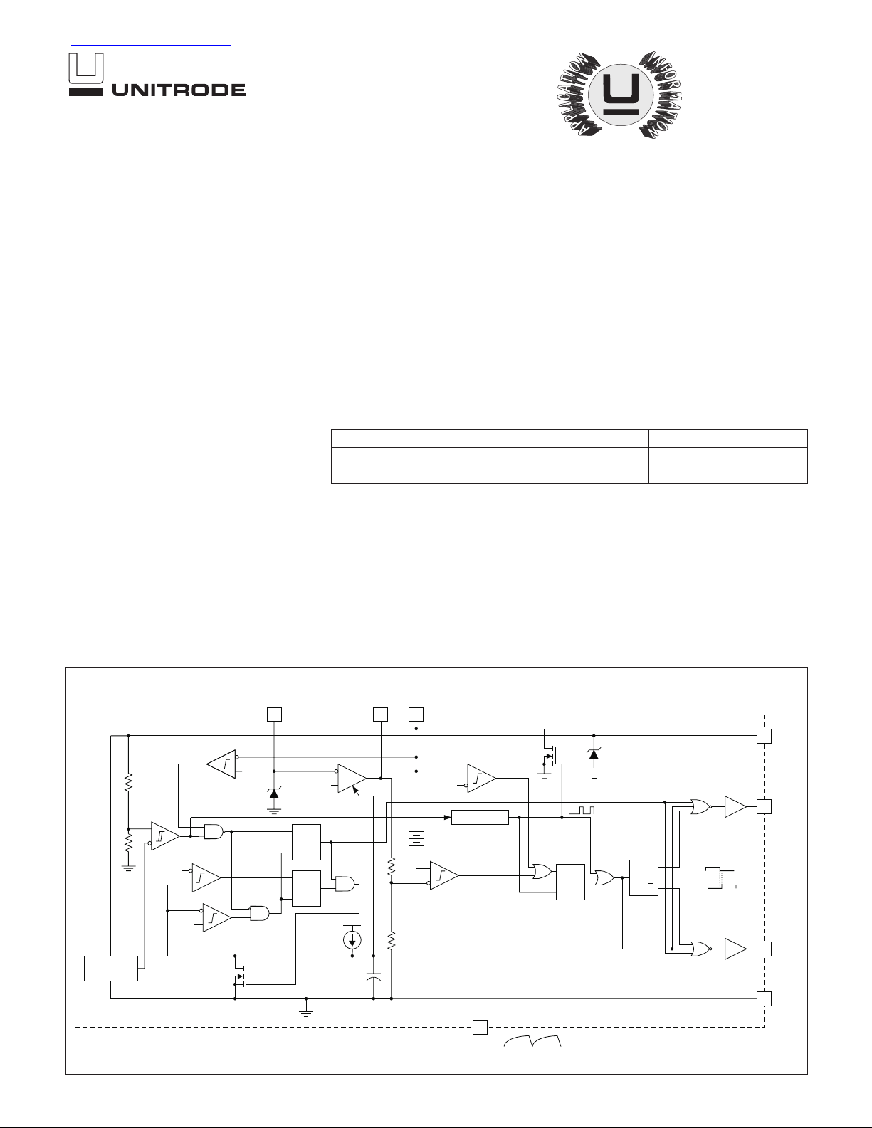
BLOCK DIAGRAM
OVERCURRENT
COMPARATOR
VDD OK
VDD–1V
0.5V
VOLTAGE
REFERENCE
0.75V
SOFT START
FB COMP CS
2.0V
2.2V
S
Q
R
S
Q
R
SLOPE = 1V/ms
VDD
1.2R
R
312
PEAK CURRENT
COMPARATOR
0.5V
OSCILLATOR
0.8V
PWM
COMPARATOR
VDD
8
14V
7
OUTA
PWM
LATCH
S
Q
R
4
RC
Q
T
Q
6
OUTB
5
GND
UDG-99076
04/99
Page 2
ABSOLUTE MAXIMUM RATINGS
Supply Voltage (IDD ≤ 10mA) . . . . . . . . . . . . . . . . . . . . . . . 15V
Supply Current . . . . . . . . . . . . . . . . . . . . . . . . . . . . . . . . . 20mA
OUTA/OUTB Source Current (peak) . . . . . . . . . . . . . . . . –0.5A
OUTA/OUTB Sink Current (peak) . . . . . . . . . . . . . . . . . . . 1.0A
Analog Inputs (FB, CS) . –0.3V to VDD+0.3V, not to exceed 6V
Power Dissipation at TA = 25°C (N Package). . . . . . . . . . . . 1W
Power Dissipation at TA = 25°C (D Package) . . . . . . . . 650mW
Storage Temperature . . . . . . . . . . . . . . . . . . . –65°C to +150°C
Junction Temperature. . . . . . . . . . . . . . . . . . . –55°C to +150°C
Lead Temperature (Soldering, 10sec.) . . . . . . . . . . . . . +300°C
Currents are positive into, negative out of the specified terminal.
Consult Packaging Section of Databook for thermal limitations
and considerations of package.
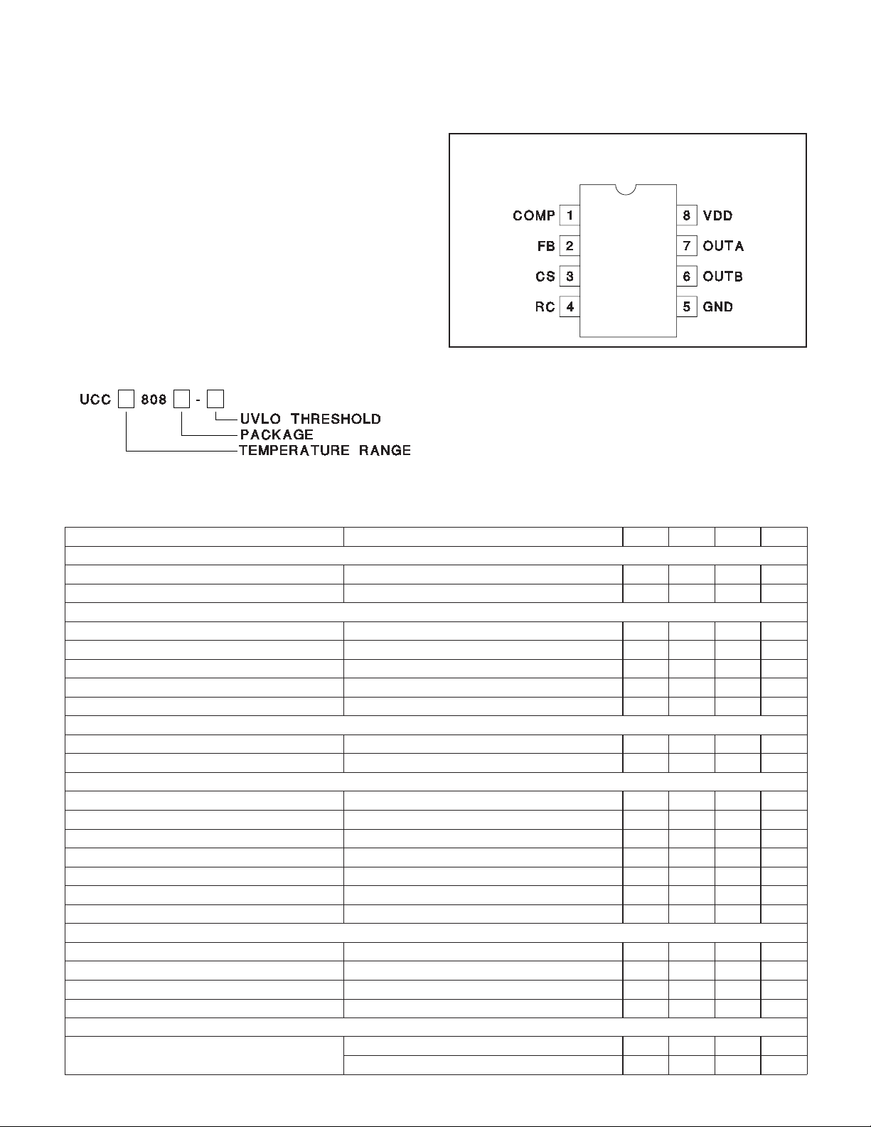
ORDER INFORMATION
UCC1808-1/-2
UCC2808-1/-2
UCC3808-1/-2
CONNECTION DIAGRAM
DIL-8, SOIC-8 (Top View)
J or N Package, D Package
ELECTRICAL CHARACTERISTICS:
the UCC2808-X and –55°C to 125°C for the UCC1808-X, VDD = 10V (Note 6), 1µF capacitor from VDD to GND, R = 22kΩ,
C = 330pF. TA=TJ.
PARAMETER TEST CONDITIONS MIN TYP MAX UNITS
Oscillator Section
Oscillator Frequency 175 194 213 kHz
Oscillator Amplitude/VDD (Note 1) 0.44 0.5 0.56 V/V
Error Amplifier Section
Input Voltage COMP = 2V 1.95 2 2.05 V
Input Bias Current –1 1 µA
Open Loop Voltage Gain 60 80 dB
COMP Sink Current FB = 2.2V, COMP = 1V 0.3 2.5 mA
COMP Source Current FB = 1.3V, COMP = 3.5V –0.2 –0.5 mA
PWM Section
Maximum Duty Cycle Measured at OUTA or OUTB 48 49 50 %
Minimum Duty Cycle COMP = 0V 0 %
Current Sense Section
Gain (Note 2) 1.9 2.2 2.5 V/V
Maximum Input Signal COMP = 5V (Note 3) 0.45 0.5 0.55 V
CS to Output Delay COMP = 3.5V, CS from 0 to 600mV 100 200 ns
CS Source Current –200 nA
CS Sink Current CS = 0.5V, RC = 5.5V (Note 7) 5 10 mA
Over Current Threshold 0.7 0.75 0.8 V
COMP to CS Offset CS = 0V 0.35 0.8 1.2 V
Output Section
OUT Low Level I = 100mA 0.5 1 V
OUT High Level I = –50mA, VDD – OUT 0.5 1 V
Rise Time C
Fall Time CL= 1nF 25 60 ns
Undervoltage Lockout Section
Start Threshold UCCx808-1 (Note 6) 11.5 12.5 13.5 V
Unless otherwise specified,TA = 0°C to 70°C for the UCC3808-X, –40°C to 85°C for
= 1nF 25 60 ns
L
UCCx808-2 4.1 4.3 4.5 V
2
Page 3
UCC1808-1/-2
UCC2808-1/-2
UCC3808-1/-2
ELECTRICAL CHARACTERISTICS:
the UCC2808-X and –55°C to 125°C for the UCC1808-X, VDD = 10V (Note 6), 1µF capacitor from VDD to GND, R = 22kΩ,
C = 330pF. TA=TJ.
PARAMETER TEST CONDITIONS MIN TYP MAX UNITS
Undervoltage Lockout Section (cont.)
Minimum Operating Voltage After Start UCCx808-1 7.6 8.3 9 V
Hysteresis UCCx808-1 3.5 4.2 5.1 V
Soft Start Section
COMP Rise Time FB = 1.8V, Rise from 0.5V to 4V 3.5 20 ms
Overall Section
Startup Current VDD < Start Threshold 130 260 µA
Operating Supply Current FB = 0V, CS = 0V (Note 5 and 6) 1 2 mA
VDD Zener Shunt Voltage IDD = 10mA (Note 4) 13 14 15 V
Note 1: Measured at RC. Signal amplitude tracks VDD.
Note 2: Gain is defined by
Note 3: Parameter measured at trip point of latch with FB at 0V.
Note 4: Start threshold and Zener Shunt threshold track one another.
Note 5: Does not include current in the external oscillator network.
Note 6: For UCCx808-1, set VDD above the start threshold before setting at 10V.
Note 7: The internal current sink on the CS pin is designed to discharge an external filter capacitor. It is not intended to be a DC
sink path.
V
∆
COMP
A
=
V
∆
CS
Unless otherwise specified,TA = 0°C to 70°C for the UCC3808-X, –40°C to 85°C for
UCCx808-2 3.9 4.1 4.3 V
UCCx808-2 0.1 0.2 0.3 V
, 0 VCS0.4V.
PIN DESCRIPTIONS
COMP: COMP is the output of the error amplifier and the
input of the PWM comparator. The error amplifier in the
UCC3808 is a true low-output impedance, 2MHz operational amplifier. As such, the COMP pin can both source
and sink current. However, the error amplifier is internally
current limited, so that zero duty cycle can be externally
forced by pulling COMP to GND.
The UCC3808 family features built-in full cycle soft start.
Soft start is implemented as a clamp on the maximum
COMP voltage.
CS: The input to the PWM, peak current, and
overcurrent comparators. The overcurrent comparator is
only intended for fault sensing. Exceeding the
overcurrent threshold will cause a soft start cycle. An internal MOSFET discharges the current sense filter capacitor to improve dynamic performance of the power
converter.
FB: The inverting input to the error amplifier. For best
stability, keep FB lead length as short as possible and FB
stray capacitance as small as possible.
GND: Reference ground and power ground for all functions. Due to high currents, and high frequency operation
of the UCC3808, a low impedance circuit board ground
plane is highly recommended.
OUTA and OUTB: Alternating high current output
stages. Both stages are capable of driving the gate of a
power MOSFET. Each stage is capable of 500mA peak
source current, and 1A peak sink current.
The output stages switch at half the oscillator frequency,
in a push/pull configuration. When the voltage on the RC
pin is rising, one of the two outputs is high, but during fall
time, both outputs are off. This “dead time” between the
two outputs, along with a slower output rise time than fall
time, insures that the two outputs can not be on at the
same time. This dead time is typically 60ns to 200ns and
depends upon the values of the timing capacitor and resistor.
The high-current output drivers consist of MOSFET output devices, which switch from VDD to GND. Each output stage also provides a very low impedance to
overshoot and undershoot. This means that in many
cases, external schottky clamp diodes are not required.
RC: The oscillator programming pin. The UCC3808’s oscillator tracks VDD and GND internally, so that variations
in power supply rails minimally affect frequency stability.
Fig. 1 shows the oscillator block diagram.
Only two components are required to program the oscillator, a resistor (tied to the VDD and RC), and a capacitor (tied to the RC and GND). The approximate oscillator
frequency is determined by the simple formula:
3
Page 4

PIN DESCRIPTIONS (cont.)
f
OSCILLATOR
where frequency is in Hertz, resistance in Ohms, and capacitance in Farads. The recommended range of timing
resistors is between 10kΩ and 200kΩ and range of timing capacitors is between 100pF and 1000pF. Timing resistors less than 10kΩ should be avoided.
For best performance, keep the timing capacitor lead to
GND as short as possible, the timing resistor lead from
VDD as short as possible, and the leads between timing
components and RC as short as possible. Separate
ground and VDD traces to the external timing network
are encouraged.
141.
=
RC
UCC1808-1/-2
UCC2808-1/-2
UCC3808-1/-2
VDD: The power input connection for this device. Al-
though quiescent VDD current is very low, total supply
current will be higher, depending on OUTA and OUTB
current, and the programmed oscillator frequency. Total
VDD current is the sum of quiescent VDD current and
the average OUT current. Knowing the operating frequency and the MOSFET gate charge (Qg), average
OUT current can be calculated from
= Qg • F, where F is frequency.
I
OUT
To prevent noise problems, bypass VDD to GND with a
ceramic capacitor as close to the chip as possible along
with an electrolytic capacitor. A 1µF decoupling capacitor
is recommended.
UDG-97009
The oscillator generates a sawtooth waveform on RC. During the RC rise time, the output stages alternate on time, but both
stages are off during the RC fall time. The output stages switch a ½ the oscillator frequency, with guaranteed duty cycle of <
50% for both outputs.
Figure 1. Block diagram for oscillator.
APPLICATION INFORMATION
A 200kHz push-pull application circuit with a full wave rectifier is shown in Fig. 2. The output, VO, provides 5V at
75W maximum and is electrically isolated from the input.
Since the UCC3808 is a peak current mode controller the
2N2222A emitter following amplifier (buffers the CT waveform) provides slope compensation which is necessary
for duty ratios greater than 50%. Capacitor decoupling is
very important with a single ground IC controller and a
1µF is suggested as close to the IC as possible. The controller supply is a series RC for startup, paralleled with a
bias winding on the output inductor used in steady state
operation.
Isolation is provided by an optocoupler with regulation
done on the secondary side using the UC3965 Precision
Reference with Low Offset Error Amplifier. Small signal
compensation with tight voltage regulation is achieved
using this part on the secondary side. Many choices exist for the output inductor depending on cost, volume,
and mechanically strength. Several design options are
iron powder, molypermalloy (MPP), or a ferrite core with
an air gap as shown here. The main power transformer
is a low profile design, EFD size 25, using Magnetics
Inc. P material which is a good choice at this frequency
and temperature. The input voltage may range from 36V
dc to 72V dc. Refer to application note U-170 for addition design information.
4
Page 5

APPLICATION INFORMATION (cont.)
–
+
O
V
5V 75W
26.1kΩ
49.9kΩ
UCC1808-1/-2
UCC2808-1/-2
UCC3808-1/-2
26.1kΩ
GROUND
SECONDARY
SOFT-START
RC
866Ω
3
2
U3
MOC8102
4
5
4.99kΩ
4.99kΩ
4321
20kΩ
1kV
0.01µF
1
6
301kΩ
(OPTIONAL)
432Ω
330pF
LOOP A
COMP
1000pF
21.0kΩ
4700pF
1.0µF
2.7Ω
IRF640
390pF
U1
UC3965DP
100pF
1N4148
8
1
1N4148
CLOSED-LOOP
10kΩ
7
6
2
3
10Ω
1N4148
2.2Ω
5
4
1.0µF
GROUND
PRIMARY
5678
1.0µF
LOOP B
0.01µF
EF25 8:24 680µF
S2
NS1N
32CTQ030EFD25
10:2
P1
P2
N
N
BYV
28-200
62Ω62Ω
BYV
28-200
1000pF
56kΩ
1N5244
0.47µF4700µF
+
–
IN
V
36V TO 72V
Figure 2. Typical application diagram.
14V
IRF640
UCC3808D-1
2N2222A
0.05Ω2kΩ
2.2Ω
330pF
0.1µF47µF
CURRENT
SENSE
97.6kΩ
2kΩ
UDG-97010-1
5
Page 6

TYPICAL CHARACTERISTIC CURVES
1000
100
10
FREQUENCY (kHz)
1
0 50 100 150 200 250
Figure 3. Typical oscillator frequency.
TIMING RESISTOR, RT (kOhms)
CT=100pF
CT=220pF
CT=330pF
CT=560pF
CT=820pF
CT=1000pF
UCC1808-1/-2
UCC2808-1/-2
UCC3808-1/-2
180
160
140
120
100
80
60
40
PHASE MARGIN (DEGREES)
20
0
1 100 10000 1000000
FREQUENCY (Hz)
Figure 6. Typical error amplifier response.
PHASE
GAIN
90
80
70
60
50
40
30
20
10
0
AC GAIN (dB)
14
VDD = 10v, T = +25°C
12
10
8
6
IDD (mA)
4
2
0
0 200 400 600 800 1000 1200
OSCILLATOR FREQUENCY (kHz)
Figure 4. Typical IDDactive current.
1.2
1
0.8
0.6
IDD
with 1nF load
IDD
without load
120
100
80
60
DEAD TIME (ns)
40
20
0
0 20406080100
TIMING RESISTOR (RT) kOhms
CT=1000pF
CT=820pF
CT=560pF
CT=330pF
CT=220pF
CT=100pF
Figure 7. Typical dead time between output stages.
0.4
0.2
COMP – CS OFFSET (V)
0
-55 -35 -15 5 25 45 65 85 105 125
TEMPERATURE (°C)
Figure 5. Typical COMP to CS offset vs. temperature.
UNITRODE CORPORATION
7 CONTINENTALBLVD. • MERRIMACK, NH 03054
TEL. (603) 424-2410 FAX (603) 424-3460
6
Page 7

IMPORTANT NOTICE
T exas Instruments and its subsidiaries (TI) reserve the right to make changes to their products or to discontinue
any product or service without notice, and advise customers to obtain the latest version of relevant information
to verify, before placing orders, that information being relied on is current and complete. All products are sold
subject to the terms and conditions of sale supplied at the time of order acknowledgement, including those
pertaining to warranty, patent infringement, and limitation of liability.
TI warrants performance of its semiconductor products to the specifications applicable at the time of sale in
accordance with TI’s standard warranty. Testing and other quality control techniques are utilized to the extent
TI deems necessary to support this warranty . Specific testing of all parameters of each device is not necessarily
performed, except those mandated by government requirements.
CERTAIN APPLICATIONS USING SEMICONDUCTOR PRODUCTS MAY INVOLVE POTENTIAL RISKS OF
DEATH, PERSONAL INJURY, OR SEVERE PROPERTY OR ENVIRONMENTAL DAMAGE (“CRITICAL
APPLICATIONS”). TI SEMICONDUCTOR PRODUCTS ARE NOT DESIGNED, AUTHORIZED, OR
WARRANTED TO BE SUITABLE FOR USE IN LIFE-SUPPORT DEVICES OR SYSTEMS OR OTHER
CRITICAL APPLICA TIONS. INCLUSION OF TI PRODUCTS IN SUCH APPLICATIONS IS UNDERST OOD TO
BE FULLY AT THE CUSTOMER’S RISK.
In order to minimize risks associated with the customer’s applications, adequate design and operating
safeguards must be provided by the customer to minimize inherent or procedural hazards.
TI assumes no liability for applications assistance or customer product design. TI does not warrant or represent
that any license, either express or implied, is granted under any patent right, copyright, mask work right, or other
intellectual property right of TI covering or relating to any combination, machine, or process in which such
semiconductor products or services might be or are used. TI’s publication of information regarding any third
party’s products or services does not constitute TI’s approval, warranty or endorsement thereof.
Copyright 1999, Texas Instruments Incorporated
 Loading...