

Page 1
查询UCC1810供应商
Dual Channel Synchronized Current Mode PWM
UCC1810
UCC2810
UCC3810
FEATURES
• Single Oscillator Synchronizes Two
PWMs
• 150
• 2mA Operating Supply Current
• Operation to 1MHz
• Internal Soft Start
• Full-Cycle Fault Restart
• Internal Leading Edge Blanking of the
• 1 Amp Totem Pole Outputs
• 75ns Typical Response from Current
• 1.5% Tolerance Voltage Reference
A Startup Supply Current
Current Sense Signal
Sense to Output
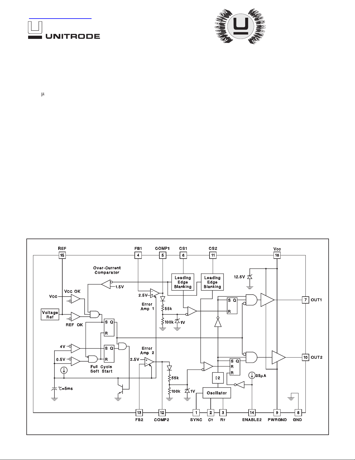
BLOCK DIAGRAM
DESCRIPTION
The UCC3810 is a high-speed BiCMOS integrated circuit which implements two synchronized pulse width modulators for use in off-line and
DC-to-DC power supplies.
The UCC3810 provides perfect synchronization between two PWMs by using the same oscillator. The oscillator’s sawtooth waveform can be used for
slope compensation if required.
Using a toggle flip flop to alternate between modulators, the UCC3810 ensures that one PWM will not slave, interfere, or otherwise affect the other
PWM. This toggle flip flop also ensures that each PWM will be limited to
50% maximum duty cycle, insuring adequate off-time to reset magnetic elements.
This IC contains many of the same elements of the UC3842 current mode
controller family, combined with the enhancements of the UCC3802. This
minimizes power supply parts count. Enhancements include leading edge
blanking of the current sense signals, full cycle fault restart, CMOS output
drivers, and outputs which remain low even when the supply voltage is removed.
02/99
UDG-92062-1
Page 2
ABSOLUTE MAXIMUM RATINGS
VCCVoltage (Note 3). . . . . . . . . . . . . . . . . . . . . . . . . . . . . . 11V
VCCCurrent . . . . . . . . . . . . . . . . . . . . . . . . . . . . . . . . . . . 20mA
OUT1, OUT2 Current, Peak, 5% Duty Cycle. . . . . . . . . . . .±1A
OUT1, OUT2 Energy (Capacitive Load) . . . . . . . . . . . . . . 20µJ
Analog Inputs (FB1, FB2, CS1, CS2, SYNC). . . . –0.3V to 6.3V
Operating Junction Temperature. . . . . . . . . . . . . . . . . . +150°C
Storage Temperature Range . . . . . . . . . . . . . –65°C to +150°C
Lead Temperature (Soldering, 10 seconds) . . . . . . . . . . 300°C
UCC1810
UCC2810
UCC3810
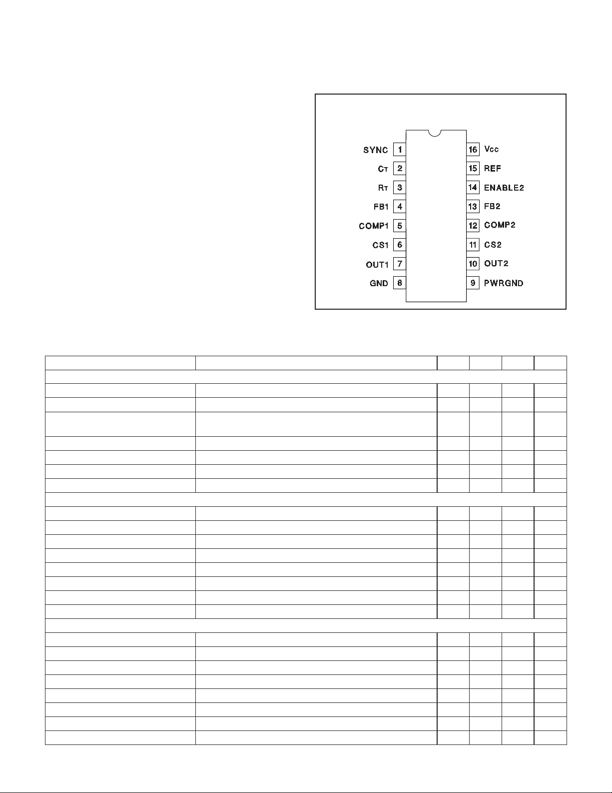
CONNECTION DIAGRAM
DIL-16, SOIC-16 (TOP VIEW)
J or N Package, DW Package
Note 1: All voltages are with respect to GND. All currents are
positive into the specified terminals.
Note 2: Consult Unitrode Integrated Circuits Product & Appli-
cations Handbook for information regarding thermal
specifications and limitations of packages.
Note 3: In normal operation, V
is powered through a current
CC
limiting resistor. Absolute maximum of 11V applies
when driven from a low impedance such that the V
CC
current does not exceed 20mA.
ELECTRICAL CHARACTERISTICS:
UCC1810; –40°C≤T
85°C for UCC2810; 0°C≤T
≤
A
Unless otherwise stated, these specifications apply for –55°C≤T
70°C for UCC3810; V
≤
A
= 10V (Note 4); RT= 150k; CT= 120pF;
CC
125°C for
≤
A
No Load; TA= TJ. All parameters are the same for both channels.
PARAMETER TEST CONDITIONS MIN TYP MAX UNITS
Reference Section
Output Voltage T
Load Regulation 0mA < I
Line Regulation UVLO Stop Threshold Voltage +0.5V < VCC< Shunt
= 25°C 4.925 5.000 5.075 V
J
< 5mA 5 25 mV
REF
12 mV
Voltage
Output Voltage Full temperature range, 0mA < I
< 5mA 4.85 5.00 5.10 V
REF
Output Noise Voltage 10Hz < f < 10kHz, TJ= +25°C (Note 10) 235 µV
Long Term Stability TA= +125°C, 1000 Hours (Note 10) 5 mV
Output Short Circuit Current –8 –25 mA
Oscillator Section
Oscillator Frequency R
= 30k, CT= 120pF (Note 5) 840 940 1040 kHz
T
Oscillator Frequency RT= 150k, CT= 120pF (Note 5) 200 220 240 kHz
Temperature Stability (Note 10) 2.5 %
Peak Voltage 2.5 V
Valley Voltage 0.05 V
Peak-to-Peak Amplitude 2.25 2.45 2.65 V
SYNC Threshold 0.80 1.65 2.2 V
SYNC Input Current SYNC = 5V 30 µA
Error Amplifier Section
FB Input Voltage COMP = 2.5V 2.44 2.50 2.56 V
FB Input Bias Current ±1 µA
Open Loop Voltage Gain 60 73 dB
Unity Gain Bandwidth (Note 10) 2 MHz
COMP Sink Current FB = 2.7V, COMP = 1V 0.3 1.4 3.5 mA
COMP Source Current FB = 1.8V, COMP = 4V –0.2 –0.5 –0.8 mA
Minimum Duty Cycle COMP = 0V 0 %
COMP Soft Start Rise Time FB = 1.8V, Rise from 0.5V to REF–1.5V 5 ms
2
Page 3
UCC1810
UCC2810
UCC3810
ELECTRICAL CHARACTERISTICS:
UCC1810; –40°C≤T
85°C for UCC2810; 0°C≤T
≤
A
Unless otherwise stated, these specifications apply for –55°C≤T
70°C for UCC3810; VCC= 10V (Note 4); RT= 150k; CT= 120pF;
≤
A
125°C for
≤
A
No Load; TA= TJ. All parameters are the same for both channels.
PARAMETER TEST CONDITIONS MIN TYP MAX UNITS
Current Sense Section
Gain (Note 6) 1.20 1.55 1.80 V/V
Maximum Input Signal COMP = 5V (Note 7) 0.9 1.0 1.1 V
CS Input Bias Current
±
200 nA
CS to OUT Propagation Delay CS steps from 0V to 1.2V, COMP = 2.5V 75 ns
CS Blank Time (Note 8) 55 ns
CS Overcurrent Threshold 1.35 1.55 1.85 V
COMP to CS Offset CS = 0V 0.65 0.95 1.4 V
PWM Section
Maximum Duty Cycle R
T = 150k, CT = 120pF (Note 10) 45 49 50 %
Maximum Duty Cycle RT = 30k, CT = 120pF (Note 10) 40 45 48 %
Minimum On Time CS =1.2V, COMP = 5V 130 ns
Output Section
OUT Low Level I
OUT = 20mA 0.12 0.42 V
IOUT = 200mA 0.48 1.10 V
IOUT = 20mA, VCC = 0V 0.7 1.20 V
OUT High Level
(VCC - OUT)
OUT Rise Time C
IOUT = –20mA 0.15 0.42 V
IOUT = –200mA 1.20 2.30 V
OUT = 1nF 20 50 ns
OUT Fall Time COUT = 1nF 30 60 ns
Undervoltage Lockout Section
Start Threshold 9.9 11.3 13.2 V
Stop Threshold 7.5 8.3 9.5 V
Start to Stop Hysteresis 1.7 3.0 4.7 V
ENABLE2 Input Bias Current ENABLE2 = 0V –20 –35 –55 µA
ENABLE2 Input Threshold
0.80 1.53 2.00 V
Voltage
Overall Section
Startup Current V
Operating Supply Current,
CC < Start Threshold Voltage 0.15 0.25 mA
VCC = 10V, FB = 2.75V 2.0 3.0 mA
Outputs Off
Operating Supply Current,
CC = 10V, FB = 0V, CS = 0V, RT = 150k 3.2 5.1 mA
V
Outputs On
Operating Supply Current,
CC = 10V, FB = 0V, CS = 0V, RT = 30k 8.5 14.5 mA
V
Outputs On
CC Internal Zener Voltage ICC = 10mA (Note 9) 11.0 12.9 14.0 V
V
VCC Internal Zener Voltage Minus
0.4 1.2 V
Start Threshold Voltage
Note 4: Adjust VCCabove the start threshold before setting at 10V.
Note 5: Oscillator frequency is twice the output frequency.
VCOMP
Note 6: Current Sense Gain A is defined by:
∆
A
=≤≤
VCS
∆
F
OSC
008.
4
≈
RT CT
×
VCS V
.
Note 7: Parameter measured at trip point of latch with FB = 0V.
Note 8: CS Blank Time is measured as the difference between the minimum non-zero on-time and the CS to OUT delay.
Note 9: Start Threshold Voltage and V
Internal Zener Voltage track each other.
CC
Note 10: Guaranteed by design. Not 100% tested in production.
3
Page 4

PIN DESCRIPTIONS
COMP1, COMP2: The low impedance outputs of the er-
ror amplifiers.
CS1, CS2: The current sense inputs to the PWM com-
parators. These inputs have leading edge blanking. For
most applications, no input filtering is required. Leading
edge blanking disconnects the CS inputs from all internal circuits for the first 55ns of each PWM cycle. When
used with very slow diodes or in other applications
where the current sense signal is unusually noisy, a
small current sense RC filter may be required.
CT: The timing capacitor of the oscillator. Recommended values of C
nect the timing capacitor directly across C
ENABLE2: A logic input which disables PWM 2 when
low. This input has no effect on PWM 1. This input is internally pulled high. In most applications it can be left
floating. In unusually noisy applications, the input should
be bypassed with a 1nF ceramic capacitor. This input
has TTL compatible thresholds.
FB1, FB2: The high impedance inverting inputs of the
error amplifiers.
GND: To separate noise from the critical control circuits,
this part has two different ground connections: GND and
PWRGND. GND and PWRGND must be electrically
connected together. However, use care to avoid coupling noise into GND.
OUT1, OUT2: The high current push-pull outputs of the
PWM are intended to drive power MOSFET gates
through a small resistor. This resistor acts as both a current limiting resistor and as a damping impedance to
minimize ringing and overshoot.
are between 100pF and 1nF. Con-
T
and GND.
T
UCC1810
UCC2810
UCC3810
PWRGND: To separate noise from the critical control
circuits, this part has two different ground connections:
GND and PWRGND. GND and PWRGND must be electrically connected together.
REF: The output of the 5V reference. Bypass REF to
GND with a ceramic capacitor≥0.01µF for best performance.
RT: The oscillator charging current is set by the value of
the resistor connected from R
lated to 1V, but the actual charging current is 10V/R
Recommended values of RT are between 10k and 470k.
For a given frequency, higher timing resistors give
higher maximum duty cycle and slightly lower overall
power consumption. Supply current decreases with increased R
T by the relationship:
V
ICC
11
=
RT
∆
For more information, see the detailed oscillator block
diagram.
SYNC: This logic input can be used to synchronize the
oscillator to a free running oscillator in another part. This
pin is edge triggered with TTL thresholds, and requires
at least a 10ns wide pulse. If unused, this pin can be
grounded, open circuited, or connected to REF.
VCC: The power input to the IC. This pin supplies current to all functions including the high current output
stages and the precision reference. Therefore, it is critical that V
be directly bypassed to PWRGND with an
CC
0.1µF ceramic capacitor.
T to GND. This pin is regu-
T.
APPLICATION INFORMATION
Leading Edge Blanking and Current Sense
Figure 1. shows how an external power stage is connected to the UCC3810. The gate of an external power
N-channel MOSFET is connected to OUT through a
small current limiting resistor. For most applications, a
10Ω resistor is adequate to limit peak current and also
practical at damping resonances between the gate driver
and the MOSFET input reactance. Long gate lead length
increases gate capacitance and mandates a higher series gate resistor to damp the RLC tank formed by the
lead, the MOSFET input reactance, and the UCC3810
driver output resistance.
The UCC3810 features internal leading edge blanking of
the current sense signal on both current sense inputs.
The blank time starts when OUT rises and continues for
55ns. During that 55ns period, the signal on CS is ignored. For most PWM applications, this means that the
CS input can be connected to the current sense resistor
as shown above. However, high speed grounding practices and short lead lengths are still required for good
performance.
4
Page 5

APPLICATION INFORMATION (cont.)
Figure 1. Detailed block diagram.
UCC1810
UCC2810
UCC3810
Oscillator
The UCC3810 oscillator generates a sawtooth wave at
CT. The sawtooth rise time is set by the resistor from RT
to GND. Since RT is biased at 1V, the current in RT is
1V/RT. The actual charging current is 10 times higher.
The fall time is set by an internal transistor on-resistance
of approximately 100Ω. During the fall time, all outputs
are off and the maximum duty cycle is reduced below
50%. Larger timing capacitors increase the discharge
time and reduce frequency. However, the percentage
maximum duty cycle is only a function of the timing resistor RT and the internal 100Ωdischarge resistance.
Error Amp Output Stage
The UCC3810 error amplifiers are operational amplifiers
with low output resistance and high input resistance. The
output stage of one error amplifier is shown above. This
output stage allows the error amplifier output to swing
close to GND and as high as one diode drop below 5V
with little loss in amplifier performance.
Figure 2. Oscillator. Figure 3. Error amp output stage.
5
Page 6

TYPICAL CHARACTERISTICS
UCC1810
UCC2810
UCC3810
Figure 4. Error amp and gain phase response.
Figure 5. Oscillator frequency vs. temperature.
Figure 7. Oscillator frequency vs. RTand C
Figure 8. Maximum duty cycle vs R
.
T
T.
Figure 6. ICCvs. oscillator frequency.
Figure 9. Maximum duty cycle vs. frequency.
6
Page 7

APPLICATION INFORMATION (cont.)
UCC1810
UCC2810
UCC3810
Figure 10. Typical application.
UDG-94022
UNITRODE CORPORATION
7 CONTINENTALBLVD. • MERRIMACK, NH 03054
TEL. (603) 424-2410 FAX (603) 424-3460
7
Page 8

IMPORTANT NOTICE
T exas Instruments and its subsidiaries (TI) reserve the right to make changes to their products or to discontinue
any product or service without notice, and advise customers to obtain the latest version of relevant information
to verify, before placing orders, that information being relied on is current and complete. All products are sold
subject to the terms and conditions of sale supplied at the time of order acknowledgement, including those
pertaining to warranty, patent infringement, and limitation of liability.
TI warrants performance of its semiconductor products to the specifications applicable at the time of sale in
accordance with TI’s standard warranty. Testing and other quality control techniques are utilized to the extent
TI deems necessary to support this warranty . Specific testing of all parameters of each device is not necessarily
performed, except those mandated by government requirements.
CERTAIN APPLICA TIONS USING SEMICONDUCT OR PRODUCTS MAY INVOLVE POTENTIAL RISKS OF
DEATH, PERSONAL INJURY, OR SEVERE PROPERTY OR ENVIRONMENTAL DAMAGE (“CRITICAL
APPLICATIONS”). TI SEMICONDUCTOR PRODUCTS ARE NOT DESIGNED, AUTHORIZED, OR
WARRANTED TO BE SUITABLE FOR USE IN LIFE-SUPPORT DEVICES OR SYSTEMS OR OTHER
CRITICAL APPLICA TIONS. INCLUSION OF TI PRODUCTS IN SUCH APPLICATIONS IS UNDERST OOD TO
BE FULLY AT THE CUSTOMER’S RISK.
In order to minimize risks associated with the customer’s applications, adequate design and operating
safeguards must be provided by the customer to minimize inherent or procedural hazards.
TI assumes no liability for applications assistance or customer product design. TI does not warrant or represent
that any license, either express or implied, is granted under any patent right, copyright, mask work right, or other
intellectual property right of TI covering or relating to any combination, machine, or process in which such
semiconductor products or services might be or are used. TI’s publication of information regarding any third
party’s products or services does not constitute TI’s approval, warranty or endorsement thereof.
Copyright 1999, Texas Instruments Incorporated
 Loading...