

Page 1
UC5602
SCSI Active Terminator
FEATURES DESCRIPTION
• Complies with SCSI, SCSI-2
Standards
• 10pF Channel Capacitance During
Disconnect
• Active Termination for 18 Lines
• Logic Command Disconnects all
Termination Lines
• Low Supply Current in Disconnect
Mode
• Trimmed Regulator for Accurate
Termination Current
• Current Limit and Thermal
Shutdown Protection
• 110 Ohm Termination
• Meets SCSI Hot Plugging
The UC5602 is a pi n compatible version of its predecessor, the UC5601,
and is targeted for high vol ume applicatio ns which req uire ac tive termination, but not the high performance of the UC5601. The major differences
are relaxed outpu t current and termination tolerances, and the absence of
low side clamps.
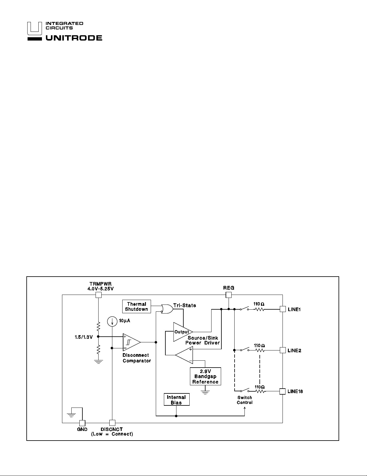
The UC5602 provides 18 lines of active termination for a SCSI (Small
Computer Systems Interface) paral lel bus. The SCSI-2 standard recommends active termination at both ends of the cable segment, and SCSI-3
will make it a requirement.
The UC5602 provides a disco nnect feature whi ch, when open ed or driven
high, will disconnect all termi nating resistors, and disables the regu lator;
greatly reduci ng standby powe r. The output channels remain high impedance even without Termpwr applied.
Internal circuit trimming is utilized, first to trim the impedance to a 7% tolerance; and then most importantly, to trim the output current 7% tolerance,
as close to the max SCSI as possible, which maximizes noise margin in
fast SCSI operation.
Other features include thermal shutdown, current limit, and 40mA of active
negation sink current capability.
BLOCK DIAGRAM
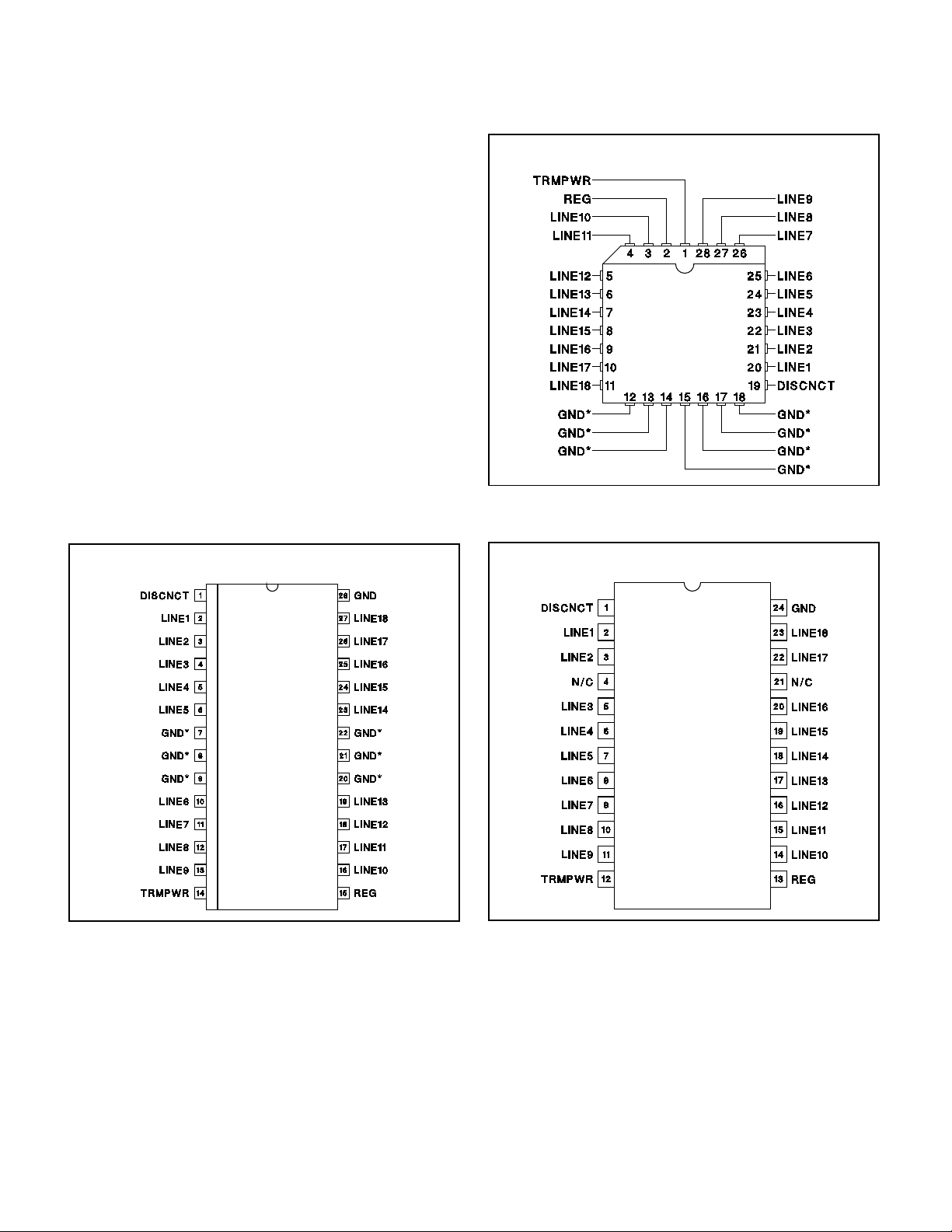
This device is offered in low thermal re sistance versions of the industry
standard 28 pin wide body SOIC and PLCC, as well as a 24 pin DIL plastic
package.
10/94
UDG-94052
Circuit Design Patented
Page 2
UC5602
ABSOLUTE MAXIMUM RATINGS
Termpwr Voltage . . . . . . . . . . . . . . . . . . . . . . . . . . . . . . . . . +7V
Signal Line Voltage. . . . . . . . . . . . . . . . . . . . . . . . . . . 0V to +7V
Regulator Output Current. . . . . . . . . . . . . . . . . . . . . . . . . . 0.5A
Storage Temperature . . . . . . . . . . . . . . . . . . . −−65°C to +150°C
Operating Tem perat ure . . . . . . . . . . . . . . . . . −−55°C t o +150° C
Lead Temperat ure (Solde ring, 10 Sec.). . . . . . . . . . . . . +300°C
Unless otherwise specified all volta ges are with respect to
Ground. Cur ren ts are po sitive into, negative out of the specified terminal.
Consult Packaging Section of Unitr ode Int egr ated Circ uits databook for thermal limitations and consider ations of pack ages .
RECOMMENDED OPERATING CONDITIONS
Termpwr Voltage . . . . . . . . . . . . . . . . . . . . . . . . . 4.0V to 5.25V
Signal Line Voltage. . . . . . . . . . . . . . . . . . . . . . . . . . . 0V to +3V
Disconnect Input Voltage . . . . . . . . . . . . . . . . . . 0V to Termpwr
SOIC-28 (Top View)
DWP Package
CONNECTION DIAGRAMS
PLCC-28 (Top View)
QP Package
* QP package pins 12 - 18 serve as both hea tsink and sign al
ground.
DIL-24 (Top View)
N Package
* DWP package pin 28 serves as signal ground ; pins 7, 8, 9,
20, 21, 22 serve as heatsink/ground.
Note: Drawings are not to scale.
2
Page 3
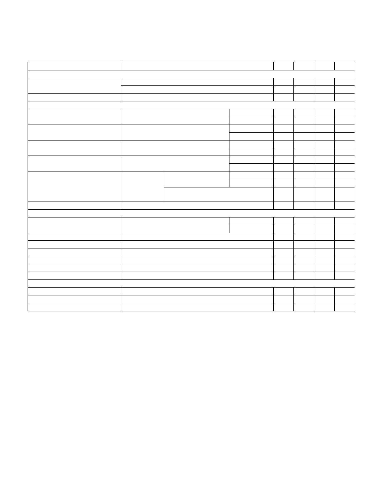
ELECTRICAL CHARACTERISTICS Unless otherwise stated, these specifications apply for TA = 0°C to 70°C.
TRMPWR = 4.75V, DISCNCT = 0V. T
PARAMETER TEST CONDITIONS MIN TYP MAX UNITS
Supply Cur rent Sect ion
Termpwr Supply Current All termination lines = Open 20 29 mA
Power Down Mode DISCNCT = Open 100 150 µA
Output Secti on (T erm inat i on Lines )
Termination Im peda nce ∆I
Output High Voltage V
Max Output Current V
Max Output Current V
Output Leakage
Output Capacit anc e DISCNCT = Open (Note 2) 10 13 pF
Regul ator Secti o n
Regulator Output Voltage T
Line Regulation TRMPWR = 4V to 6V 10 20 mV
Load Regulat io n I
Drop Out Voltage All Termination Lines = 0.5V 1.0 1.2 V
Short Circuit Cur rent V
Sinking Current Capabi lity V
Thermal Shutdow n 170 °C
Disconnect Section
Disconnect Threshold 1.1 1.4 1.7 V
Threshold Hys teres is 100 mV
Input Current DISCNCT = 0V 150 200 µA
Note 1: Measuring each term ination l ine while other 17 are low (0.5V).
Note 2: Guaranteed by design. Not 100% tested in production.
A = TJ.
All termination lines = 0.5V 400 435 mA
LINE = -5mA to -15mA TJ = 25°C 102 110 118 Ω
0°C < T
TRMPWR = 4V (Note 1) TJ = 25°C 2.6 2.9 3.1 V
0°C < T
LINE = 0.5V TJ = 25°C -19.5 -21.4 -22.4 mA
0°C < T
LINE = 0.5V, TRMPWR = 4V (Note 1) TJ = 25° C -18.0 -21.5 -22.4 mA
0°C < T
DISCNCT = 4V
TRMPWR = 0V to 5.25V
REG = 0V
V
V
TRMPWR = 0V to 5.25V, REG = Open
LINE = 0V to 5.25V
V
0°C < T
REG = 0 to -4 00mA 20 50 mV
REG = 0V -450 -650 -850 mA
REG = 3.5V 20 40 mA
J < 70°C 97 129 Ω
J < 70°C 2.55 3.2 V
J < 70°C -18.5 -22.4 mA
J < 70°C -17.0 -22.4 mA
LINE = 0 to 4V 10 400 nA
LINE = 5.25V 100 µA
10 400 nA
J = 25°C 2.7 2.9 3.1 V
J < 70°C 2.55 3.2 V
UC5602
THERMAL DATA
DWP package: (see packaging section of UICC data book for more details on thermal performance)
Thermal Resistance Junction to Leads, θjL . . . . . . . . . . . . . . . . . . . . . . . . . . . . . . . . . . . . . . . . . . . . . . 18°C/ W
Thermal Resistance Junction to Ambient, θja. . . . . . . . . . . . . . . . . . . . . . . . . . . . . . . . . . . . . . . . . . 33°-43°C/W
N package:
Thermal Resistance Junction to Leads, θjL . . . . . . . . . . . . . . . . . . . . . . . . . . . . . . . . . . . . . . . . . . . . . . 50°C/ W
Thermal Resistance Junction to Ambient, θja. . . . . . . . . . . . . . . . . . . . . . . . . . . . . . . . . . . . . . . . . 95°-105°C/W
QP package:
Thermal Resistance Junction to Leads, θjL . . . . . . . . . . . . . . . . . . . . . . . . . . . . . . . . . . . . . . . . . . . . . . 15°C/ W
Thermal Resistance Junction to Ambient, θja. . . . . . . . . . . . . . . . . . . . . . . . . . . . . . . . . . . . . . . . . . 30°-40°C/W
Note: The above n u mb ers for θjL are maximums for the limit ing ther ma l resistanc e of the packa ge in a standa rd mounting conf igu-
θ
ration. The
numbers assume no ambient airflow .
ja numbers are meant to be guidelines for the thermal per fo rmanc e of the device/pc -bo ard system . All of the abov e
3
Page 4
UC5602
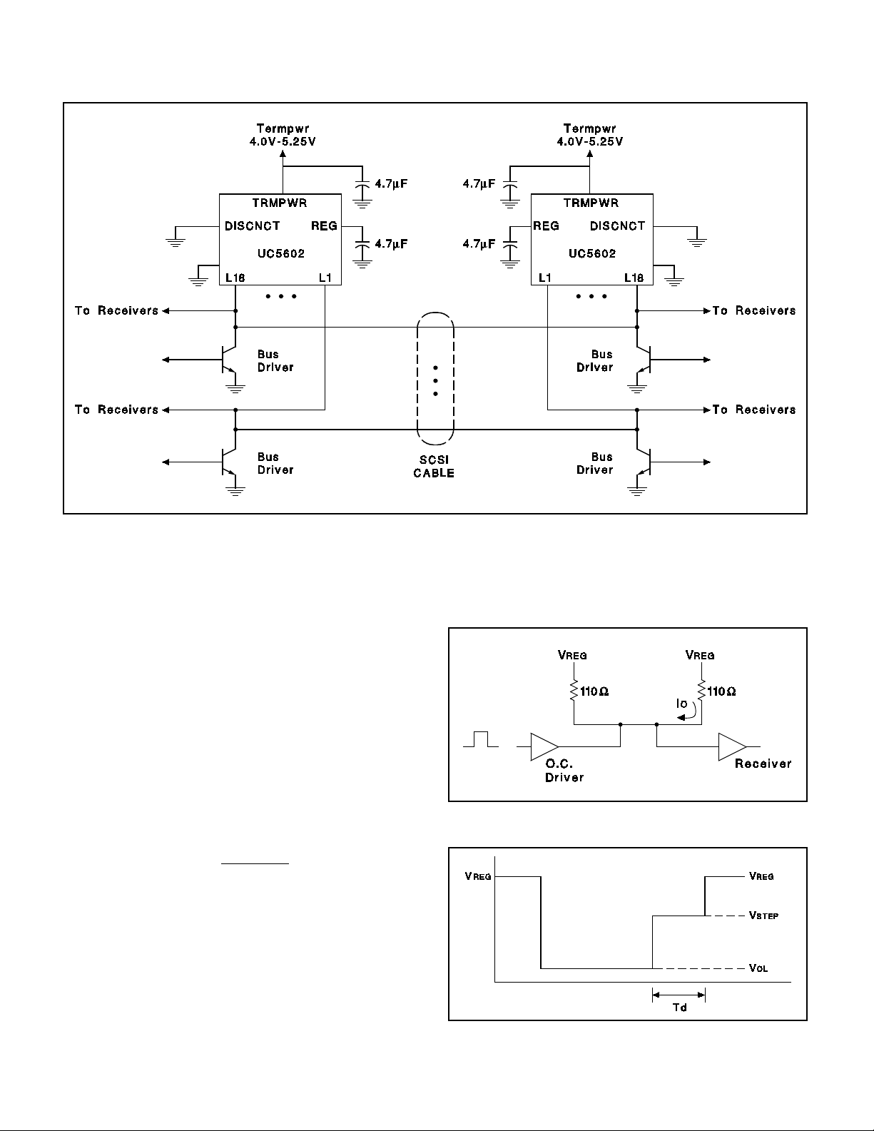
T y pical SCSI Bus Configu rati on Using t he UC5602
A Look at the Respo nse o f a SCSI-2 Cabl e
Figure 1 shows a single line of a SCSI cable. The driver
is an open colletor type which when asserted pulls low,
and when negated the termination resistance serves as
the pull -up.
Figure 2 shows a worst case scenario of mid cable deassertion with a close proximity receiver. The voltage
V
STEP is defined as:
V
STEP = VOL +IO Z0
VOL = Driver Output Low Voltage
I
O = Current from Receiving Terminator
Z
0 = Cable Characteristic Impedance
V
REG − VOL
IO =
110
In the pursui t of higher data rates, sampling could occur
during this step portion, therefore it is important to ensure
that the step is as high as possible to get the most noise
margin. For this re ason the UC5602 is trimmed so that
the output current (I
O) is as close as possible to the SCSI
max current spec of 22.4mA. The Termination impedance
is initially trimmed on the IC to 110 ohms typical, then the
regulator voltage is trimmed for the highest output current to within 22.4mA.
UDG-94053
UDG-94054
Figure 1. A Singl e L ine of a SCSI Cable
UDG-94055
Figure 2. A Typical Response of a SCSI Cable
4
Page 5
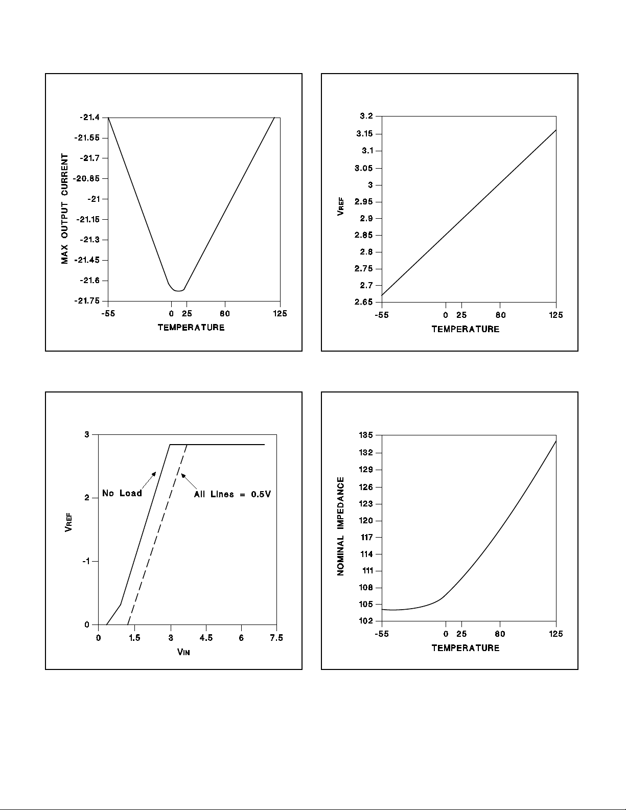
Max Output Current vs. Temperature VREF vs. Temperature
UC5602
REF vs. VIN
V
Output Impedance vs. Temperature
UNITRODE INTEGRATED CIRCUITS
7 CONTINENTAL BLVD. •• MERRIMACK, NH 03054
TEL. (603) 424-2410 • FAX (603) 424 3460
5
Page 6

PACKAGE OPTION ADDENDUM
www.ti.com
30-Mar-2005
PACKAGING INFORMATION
Orderable Device Status
(1)
Package
Type
Package
Drawing
Pins Package
Qty
Eco Plan
UC5602DWP OBSOLETE SOIC DW 28 TBD Call TI Call TI
UC5602DWPTR OBSOLETE SOIC DW 28 TBD Call TI Call TI
UC5602QP OBSOLETE PLCC FN 28 TBD Call TI Call TI
UC5602QPTR OBSOLETE PLCC FN 28 TBD Call TI Call TI
(1)
The marketing status values are defined as follows:
ACTIVE: Product device recommended for new designs.
LIFEBUY: TI has announced that the device will be discontinued, and a lifetime-buy period is in effect.
NRND: Not recommended for new designs. Device is in production to support existing customers, but TI does not recommend using this part in
a new design.
PREVIEW: Device has been announced but is not in production. Samples may or may not be available.
OBSOLETE: TI has discontinued the production of the device.
(2)
Eco Plan - The planned eco-friendly classification: Pb-Free (RoHS) or Green (RoHS & no Sb/Br) - please check
http://www.ti.com/productcontent for the latest availability information and additional product content details.
TBD: The Pb-Free/Green conversion plan has not been defined.
Pb-Free (RoHS): TI's terms "Lead-Free" or "Pb-Free" mean semiconductor products that are compatible with the current RoHS requirements
for all 6 substances, including the requirement that lead not exceed 0.1% by weight in homogeneous materials. Where designed to be soldered
at high temperatures, TI Pb-Free products are suitable for use in specified lead-free processes.
Green (RoHS & no Sb/Br): TI defines "Green" to mean Pb-Free (RoHS compatible), and free of Bromine (Br) and Antimony (Sb) based flame
retardants (Br or Sb do not exceed 0.1% by weight in homogeneous material)
(2)
Lead/Ball Finish MSL Peak Temp
(3)
(3)
MSL, Peak Temp. -- The Moisture Sensitivity Level rating according to the JEDEC industry standard classifications, and peak solder
temperature.
Important Information and Disclaimer:The information provided on this page represents TI's knowledge and belief as of the date that it is
provided. TI bases its knowledge and belief on information provided by third parties, and makes no representation or warranty as to the
accuracy of such information. Efforts are underway to better integrate information from third parties. TI has taken and continues to take
reasonable steps to provide representative and accurate information but may not have conducted destructive testing or chemical analysis on
incoming materials and chemicals. TI and TI suppliers consider certain information to be proprietary, and thus CAS numbers and other limited
information may not be available for release.
In no event shall TI's liability arising out of such information exceed the total purchase price of the TI part(s) at issue in this document sold by TI
to Customer on an annual basis.
Addendum-Page 1
Page 7

IMPORTANT NOTICE
Texas Instruments Incorporated and its subsidiaries (TI) reserve the right to make corrections, modifications,
enhancements, improvements, and other changes to its products and services at any time and to discontinue
any product or service without notice. Customers should obtain the latest relevant information before placing
orders and should verify that such information is current and complete. All products are sold subject to TI’s terms
and conditions of sale supplied at the time of order acknowledgment.
TI warrants performance of its hardware products to the specifications applicable at the time of sale in
accordance with TI’s standard warranty. Testing and other quality control techniques are used to the extent TI
deems necessary to support this warranty . Except where mandated by government requirements, testing of all
parameters of each product is not necessarily performed.
TI assumes no liability for applications assistance or customer product design. Customers are responsible for
their products and applications using TI components. To minimize the risks associated with customer products
and applications, customers should provide adequate design and operating safeguards.
TI does not warrant or represent that any license, either express or implied, is granted under any TI patent right,
copyright, mask work right, or other TI intellectual property right relating to any combination, machine, or process
in which TI products or services are used. Information published by TI regarding third-party products or services
does not constitute a license from TI to use such products or services or a warranty or endorsement thereof.
Use of such information may require a license from a third party under the patents or other intellectual property
of the third party, or a license from TI under the patents or other intellectual property of TI.
Reproduction of information in TI data books or data sheets is permissible only if reproduction is without
alteration and is accompanied by all associated warranties, conditions, limitations, and notices. Reproduction
of this information with alteration is an unfair and deceptive business practice. TI is not responsible or liable for
such altered documentation.
Resale of TI products or services with statements different from or beyond the parameters stated by TI for that
product or service voids all express and any implied warranties for the associated TI product or service and
is an unfair and deceptive business practice. TI is not responsible or liable for any such statements.
Following are URLs where you can obtain information on other Texas Instruments products and application
solutions:
Products Applications
Amplifiers amplifier.ti.com Audio www.ti.com/audio
Data Converters dataconverter.ti.com Automotive www.ti.com/automotive
DSP dsp.ti.com Broadband www.ti.com/broadband
Interface interface.ti.com Digital Control www.ti.com/digitalcontrol
Logic logic.ti.com Military www.ti.com/military
Power Mgmt power.ti.com Optical Networking www.ti.com/opticalnetwork
Microcontrollers microcontroller.ti.com Security www.ti.com/security
Telephony www.ti.com/telephony
Video & Imaging www.ti.com/video
Wireless www.ti.com/wireless
Mailing Address: Texas Instruments
Post Office Box 655303 Dallas, Texas 75265
Copyright 2005, Texas Instruments Incorporated
 Loading...