

Datasheet UC3845D1, UC3843D1, UC3844D1, UC3845, UC3844 Datasheet (Fairchild Semiconductor)
...Page 1
www.fairchildsemi.com
UC3842/UC3843/UC3844/UC3845
SMPS Controller
Features
• Low Start up Current
• Maximum Duty Clamp
• UVLO With Hysteresis
• Operating Fr equency up to 500KHz
Description
The UC3842/UC3843/UC3844/UC3845 are fixed
frequencycurrent-mode PWM controller. They are specially
designed for Off-Line and D C t o DC con ver t e r a pp l ic ati o ns
with minimum external components. These integrated
circuits feature a trimmed oscillator for precise duty cycle
control, a temperature compensated reference, high gain
error amplifier, current sensing comparator and a high
current totemp ole ou t pu t for dr ivi n g a Po we r M OSF E T. The
UC3842 and UC3844 have UVLO threshold s of 16V (on)
and 10V (off ). The UC3843 and UC3845 are 8.5V(on) and
7.9V (off). The UC3842 and UC3843 can operate within
100% duty cycle. The UC3844 and UC3845 can operate
with 50% duty cycle.
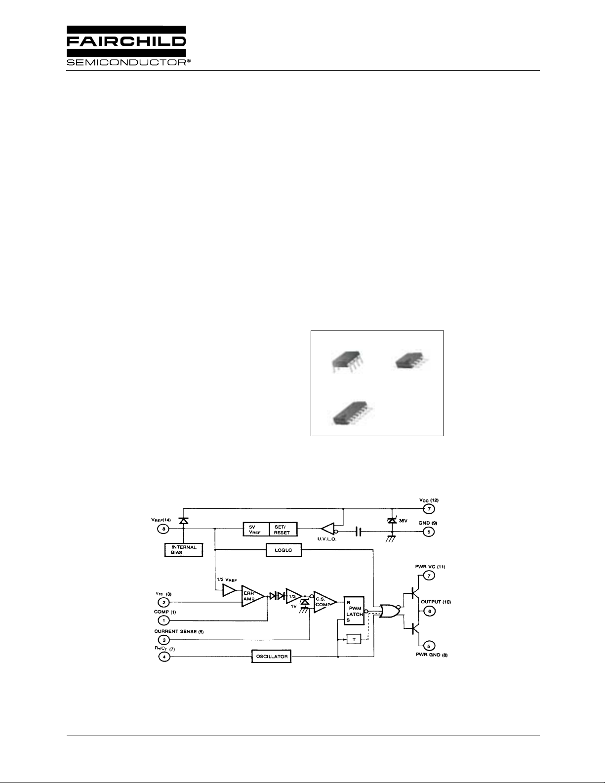
8-DIP
14-SOP
8-SOP
1
1
1
Internal Block Diagram
* NORMALLY 8DIP/8SOP PIN NO.
* ( ) IS 14SOP PINNO.
* TOGGLE FLIP FLOP USED ONLY IN UC3844, UC3845
©2002 Fairchild Semiconductor Corporation
Rev. 1.0.1
Page 2
UC3842/UC3843/UC3844/UC3845
Absolute Maximum Ratings
Parameter Symbol Value Unit
Supply Voltage V
Output Current I
Analog Inputs (Pin 2.3) V
Error Amp Output Sink Current I
Power Dissipation at T
Power Dissipation at T
Power Dissipation at T
≤25°C (8DIP) P
A
≤25°C (8SOP) P
A
≤25°C (14SOP) P
A
Storage Temperature Range T
Lead Temperature (Soldering, 10sec) T
CC
O
(ANA)
SINK (E.A)
(Note1,2) 1200 mW
D
(Note1,2) 460 mW
D
(Note1,2) 680 mW
D
STG
LEAD
Note:
1. Board Thickness 1.6mm, Board Dimension 76.2mm ×114.3mm, (Reference EIA / JS ED51-3, 51-7)
2. Do not exceeed P
and SOA (Safe Operation Area)
D
30 V
±1A
-0.3 to 6.3 V
10 mA
-65 ~ +150 °C
+300 °C
Power Dissipation Curve
1200
1200
1100
1100
1000
1000
900
900
14SOP
800
800
700
700
8SOP
8SOP
600
600
500
500
POWER DISSIPATION (mW)
POWER DISSIPATION (mW)
400
400
300
300
0 102030405060708090100110120130140150
0 102030405030 40 50 60 70 8060 70 80 90 100 11090 100 110 120 130 140120 130 140 150
14SOP
AMBIENT TEMPERATURE (℃)
AMBIENT TEMPERATURE (℃)
8DIP
8DIP
Thermal Data
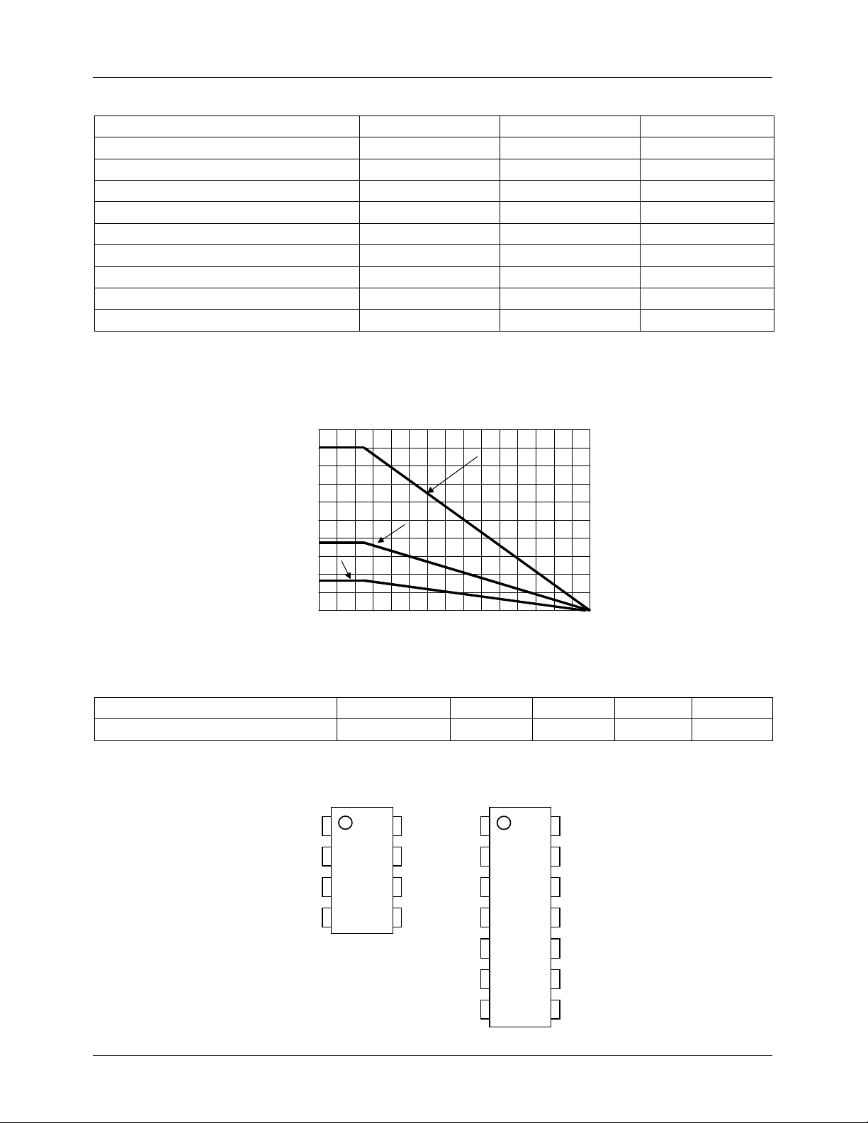
Characteristic Symbol 8-DIP 8-SOP 14-SOP Unit
Thermal Resistance Junction-ambient R
thj-amb(MAX)
100 265 180 °C/W
Pin Array
8DIP,8SOP
8DIP,8SOP
REF
REF
REF
V
V
V
8
8
COMP
COMP
COMP
CURRENT SENSE
CURRENT SENSE
CURRENT SENSE
RT/C
RT/C
RT/C
1
1
1
FB
FB
FB
V
V
V
2
2
2
3
3
3
T
T
T
4
4
4
8
7
7
7
6
6
6
5
5
5
CC
CC
CC
V
V
V
OUTPUT
OUTPUT
OUTPUT
GND
GND
GND
COMP
COMP
COMP
CURRENT SENSE 5
CURRENT SENSE 5
CURRENT SENSE 5
2
N/C 2
N/C 2
N/C 2
N/C
N/C
N/C
N/C
N/C
N/C
T/CT
T/CT
T/CT
R
R
R
14SOP
14SOP
14
14
14
REF
REF
13
13
13
12
12
12
11
11
11
10
10
10
9
9
9
8
8
8
REF
V
V
V
N/C
N/C
N/C
CC
CC
CC
V
V
V
PWR V
PWR V
PWR V
OUTPUT
OUTPUT
OUTPUT
GND
GND
GND
PWR GND
PWR GND
PWR GND
C
C
C
1
1
1
FB
FB
FB
V
V
V
3
3
3
4
4
4
6
6
6
7
7
7
Page 3
UC3842/UC3843/UC3844/UC3845
Electrical Characteristics
(VCC=15V, RT=10kΩ, CT=3.3nF, TA= 0°C to +70°C, unless otherwise specified)
Parameter Symbol Conditions Min. Typ. Max. Unit
REFERENCE SECTION
Reference Output Voltage V
Line Regulation ∆V
Load Regulation ∆V
Short Circuit Output Current I
REF
REF
REF
SC
OSCILLATOR SECTION
Oscillation Frequency f T
Frequency Change with
Voltage
Oscillator Amplitude V
∆f/∆V
OSC
ERROR AMPLIFIER SECTION
Input Bias Current I
Input Voltage V
Open Loop Voltage Gain G
BIAS
I(E>A)
VO
Power Supply Rejection Ratio PSRR 12V ≤ V
Output Sink Current I
Output Source Current I
High Output Voltage V
Low Output Voltage V
SINK
SOURCE
OH
OL
CURRENT SENSE SECTION
Gain G
Maximum Input Signal V
I(MAX)
Power Supply Rejection Ratio PSRR 12V ≤ V
Input Bias Current I
BIAS
OUTPUT SECTION
V
Low Output Voltage
High Output Voltage
Rise Time t
Fall Time t
OL
V
OH
R
F
UNDER-VOLTAGE LOCKOUT SECTION
Start Threshold
Min. Operating Voltage
(After Turn On)
V
TH(ST)
V
OPR(MIN)
TJ = 25°C, I
12V ≤ V
1mA ≤ I
CC
REF
= 1mA 4.90 5.00 5.10 V
REF
≤ 25V - 6 20 mV
≤ 20mA - 6 25 mV
TA = 25°C - -100 -180 mA
= 25°C475257kHz
J
CC
12V ≤ V
≤ 25V - 0.05 1 %
CC
- -1.6-V
- --0.1-2µA
V
= 2.5V 2.42 2.50 2.58 V
pin1
2V ≤ V
V
pin2
V
pin2
V
pin2
V
pin2
(Note 1 & 2) 2.85 3 3.15 V/V
V
V
pin1
≤ 4V (Note3) 65 90 - dB
O
≤ 25V (Note3) 60 70 - dB
CC
= 2.7V, V
= 2.3V, V
= 1.1V 2 7 - mA
pin1
= 5V -0.6 -1.0 - mA
pin1
= 2.3V, RL = 15kΩ to GND 5 6 - V
= 2.7V, RL = 15kΩ to Pin 8 - 0.8 1.1 V
= 5V(Note 1) 0.9 1 1.1 V
≤ 25V (Note 1,3) - 70 - dB
CC
- --3-10µA
I
= 20mA - 0.08 0.4 V
SINK
= 200mA - 1.4 2.2 V
I
SINK
I
SOURCE
I
SOURCE
= 20mA 13 13.5 - V
= 200mA 12 13.0 - V
TJ = 25°C, CL= 1nF (Note 3) - 45 150 ns
TJ = 25°C, CL= 1nF (Note 3) - 35 150 ns
UC3842/UC3844 14.5 16.0 17.5 V
UC3843/UC3845 7.8 8.4 9.0 V
UC3842/UC3844 8.5 10.0 11.5 V
UC3843/UC3844 7.0 7.6 8.2 V
P-P
3
Page 4
UC3842/UC3843/UC3844/UC3845
Electrical Characteristics
(Continued)
(VCC=15V, RT=10kΩ, CT=3.3nF, TA= 0°C to +70°C, unless otherwise specified)
Parameter Symbol Conditions Min. Typ. Max. Unit
PWM SECTION
Max. Duty Cycle
Min. Duty Cycle D
D
D
(Max)
(Max)
(MIN)
UC3842/UC3843 95 97 100 %
UC3844/UC3845 47 48 50 %
- --0%
TOTAL STANDBY CURRENT
Start-Up Current I
Operating Supply Current I
Zener Voltage V
Adjust V
Note:
1. Parameter measured at trip point of latch
2. Gain defined as:
A
3. These parameters, although guaranteed, are not 100 tested in production.
above the start threshould before setting at 15V
CC
∆V
pin1
----------------- -=
∆V
pin3
,0 ≤ V
pin3
≤ 0.8V
ST
CC(OPR)
Z
V
pin3=Vpin2
ICC = 25mA 30 38 - V
- -0.451mA
=ON - 14 17 mA
UC3842
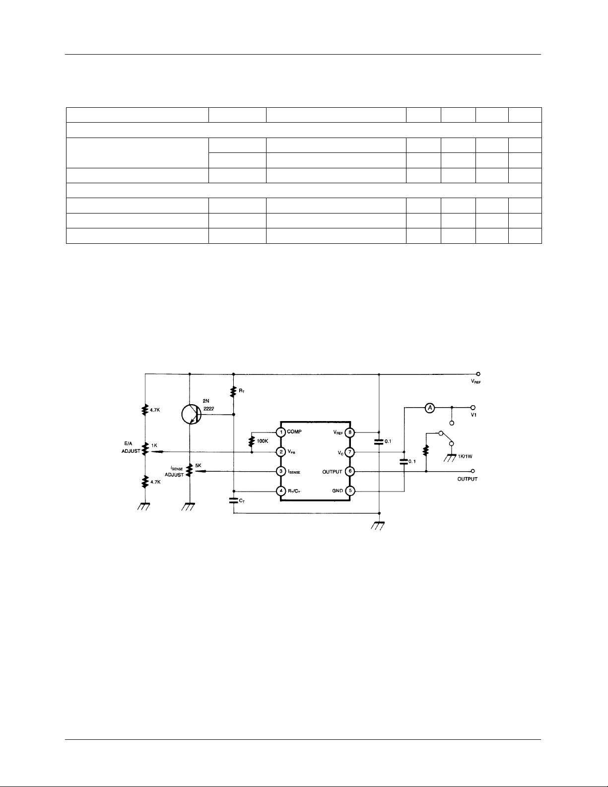
Figure 1. Open Loop Test Circuit
High peak currents associated with capacitive loads necessitate careful grounding techniques Timing and bypass capacitors
should be c onnected close to pin 5 in a single point ground. The transistor and 5kΩ potentiometer are used to sample the
oscillator waveform and apply an adjustable ramp to pin 3.
4
Page 5

UC3842/UC3843/UC3844/UC3845
UC3842/44
UC3843/45
Figure 2. Under Voltage Lockout
During Under- Voltage Lock-Out, the o utp ut drive r is bia sed to a hig h impe dance sta te. P in 6 s hould be shunt ed to grou nd with
a bleeder resistor to prevent activating the power switch with output leakage current.
Figure 3. Error Amp Configuration
Figure 4. Current Sense Circuit
Peak current (IS) is determined by the formula:
ISMAX()
1.0V
------------=
R
S
A small RC filter may be required to suppress switch transients.
5
Page 6

UC3842/UC3843/UC3844/UC3845
Figure 5. Oscillator Waveforms and Maximum Duty Cycle
Oscillator timing capacitor, CT, is charged by V
discharge time, the internal clock signal blanks the output to the low state. Selection of R
through RT and discharged by an internal current source. During the
REF
and C
T
therefore determines both
T
oscillator frequency and maximum duty cycle. Charge and discharge times are determined by the formulas:
t
= 0.55 RT C
c
tDRTCTI
=
Frequency, then, is: f=(tc + td)
ForRT 5KΩ f
T
0.0063RT2.7–
--------------------------------------- -
n
0.0063R
Figure 6. Oscillator Dead Time & Frequency Figure 7. Timing Resistance vs Frequency
-------------- -=,>
R
1.8
TCT
4–
T
-1
(Deadtime vs CT RT > 5kΩ)
Figure 8. Shutdown Techniques
6
Page 7

UC3842/UC3843/UC3844/UC3845
Shutdown of the UC3842 can be accomplished by two methods; either raise pin 3 above 1V or pull pin 1 below a voltage two
diode drops above gro und. E ither m ethod cause s the ou tput o f the PWM compa rato r to be hig h (refe r to bl ock di agra m). The
PWM latch is reset dominant so that the output will remain low until the next clock cycle after the shutdown condition at pins
1 and/or 3 is r e mo ve d. In one example, an externa l ly latched shutdown may be a cco mplished by adding an SCR whic h will be
reset by cycling V
below the lower UVLO threshold. At this point the reference turns off, allowing the SCR to reset.
CC
UC3842/UC3843
Figure 9. Slope Compensation
A fraction of the oscillator ramp can be resistively summed with the current sense signal to provide slope compensation for
converters requiring duty cycles over 50%. Note that capacitor, C
, forms a filter with R2 to suppress the leading edge switch
T
spikes.
Temperature (°C)
Figure 10. Tempera ture Drift (V ref)
Temperature (°C)
Figure 12. Temperature Drift (Icc)
Temperature (°C)
Figure 11. Temperature Drift (Ist)
7
Page 8

UC3842/UC3843/UC3844/UC3845
Mechanical Dimensions
Package
6.40
±0.20
0.252
±0.008
8-DIP
0.79
0.031
()
±0.10
±0.004
±0.10
±0.004
#1
#8
#4 #5
7.62
0.300
MAX
9.60
0.378
5.08
0.200
3.40
0.134
±0.20
9.20
MAX
±0.20
±0.008
±0.008
0.362
0.33
0.013
MIN
0.46
3.30
0.130
2.54
±0.30
±0.012
0.018
0.100
1.524
0.060
+0.10
0.25
–0.05
+0.004
0.010
–0.002
0~15°
8
Page 9

UC3842/UC3843/UC3844/UC3845
Mechanical Dimensions
Package
#1
#4
6.00 ±0.30
0.006
0.15
0.236 ±0.012
(Continued)
8-SOP
1.55 ±0.20
0.061 ±0.008
#8
#5
0.071
MAX
5.13
1.80
0.202
4.92 ±0.20
MAX
0.194 ±0.008
MIN
0.004~0.001
1.27
0.1~0.25
0.56
0.022
()
0.41 ±0.10
0.050
0.016 ±0.004
+
-0.002
-0.05
0.004
0.50 ±0.20
0.020 ±0.008
+
0.10
3.95 ±0.20
0.156 ±0.008
5.72
0.225
0~8°
MAX0.10
MAX0.004
9
Page 10

UC3842/UC3843/UC3844/UC3845
Mechanical Dimensions
Package
#1
(Continued)
14-SOP
#14
1.55
0.061
MAX
8.70
0.343
±0.10
±0.004
±0.20
8.56
±0.008
0.337
MIN
0.05
0.002
0.47
()
0.10
0.004
-0.05
+
+
0.406
0.016
0.019
-0.002
0.10
+
-0.05
0.20
0.60
0.024
0.004
+
-0.002
0.008
±0.20
±0.008
#7
6.00
0.236
3.95
0.156
5.72
0.225
±0.30
±0.012
±0.20
±0.008
#8
0~8°
1.80
0.071
MAX
MAX0.10
MAX0.004
1.27
0.050
10
Page 11

Ordering Information
Product Number Package Operating Temperature
UC3842N
UC3843N
UC3844N
UC3845N
UC3842D1
UC3843D1
UC3844D1
UC3845D1
UC3842D
UC3843D
UC3844D
UC3845D
8-DIP
8-SOP
14-SOP
UC3842/UC3843/UC3844/UC3845
0 ~ + 70°C
11
Page 12

UC3842/UC3843/UC3844/UC3845
DISCLAIMER
FAIRCHILD SEMICONDUCTOR RESERVES THE RIGHT TO MAKE CHANGES WITHOUT FURT HER NOTICE TO ANY
PRODUCTS HEREI N TO IMPROVE RELIABILITY, FUNCTIO N OR DESIGN. FAIRCH IL D DOES NOT ASSUME ANY
LIABILITY ARISING OUT OF THE APPLICATION OR USE OF ANY PRODUCT OR CIRCUIT DESCRIBED HEREIN; NEITHER
DOES IT CONVEY ANY LICENSE UNDER IT S PATENT RIGHTS, NOR THE RIGHTS OF OTHE RS.
LIFE SUPPORT POL I CY
FAIRCHILD’S PR ODUCTS ARE NOT AUTH ORIZED FOR USE AS C RITICAL COMPONENT S IN LIFE SUPPORT DE VICES
OR SYSTEMS WITHOUT THE EXPRESS WRITTEN APPROVAL OF THE PRESIDENT OF FAIRCHILD SEMICONDUCTOR
CORPORATION. As used herein :
1. Life support devices or systems are devices or systems
which, (a) are intended for surgical implant into the body,
or (b) support or sustain life, and (c) whose failure to
perform when properly used in accordance with
2. A critical component in any component of a life support
device or sy stem whose fai lure to perform can be
reasonably expec ted to cause the failur e of the life support
device or system, or to affect its safety or effec t iv ene ss .
instructions for use provided in the labeling, can be
reasonably expected to result in a significant injury of the
user.
www.fairchildsemi.com
2/19/02 0.0m 001
2002 Fairchild Semiconductor Corporation
Stock#DSxxxxxxxx
 Loading...