

Page 1
UC3842A/UC3843A
SMPS Controller
www.fairchildsemi.com
Features
• Low Start Current 0.2mA (typ)
• Operating R ange Up To 500KHz
• Cycle by Cycle Current Limiting
• Under Voltage Lock Out With Hysteresis
• Short Shutdown Delay Time: typ.100ns
• High Current Totem-pole Output
• Output Swing Lim i ti ng: 22 V
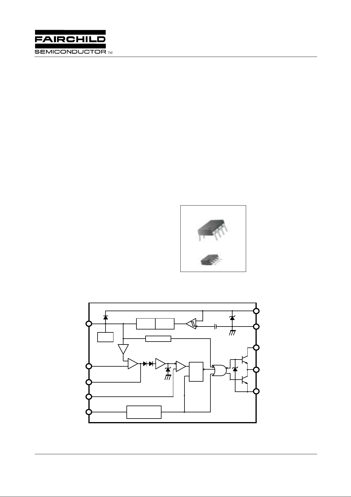
Internal Block Diagram
Description
The UC3842A/UC 38 43A ar e fixe d P WM co ntrol ler for O f fLine and DC to DC converter applications. The internal circuits include UVLO, low start up current circuit, temperature compensated reference, high gain error amplifier,
current sensing comp a ra to r, and high current totem-pole output for driving a POWER MOSFET. Also UC3842A/
UC3843A provide low start up current below 0.3mA and
short shutdown delay time typ. 100ns. The UC3842A has
UVLO thresho ld o f 16V (on ) an d 10V (of f ). Th e U C3843 A i s
8.4V(on) and 7.6V(off). The UC3842A and UC3843A c an
operate within 100% duty cycle.
8-DIP
1
8-SOP
1
8
REF
V
Internal
Bias
1/2V
REF
2
FB
V
1
COMP
3
C.S
T/CT
R
4
©2000 Fairchild Semiconductor International
5V
V
Error Amp
+
-
OSCILLATOR
RESET
REF
Good LOGIC
1/3
SET/
1V
C.S
Comp.
UVLO
PWM
LATCH
R
S
T
29V
22V
7
V
5
GND
PWR
7
V
6
OUTPUT
PWR
5
GND
CC
C
Rev. 5.0
Page 2
UC3842A/UC3843A
Absolute Maximum Ratings
Parameter Symbol Value Unit
Supply Voltage V
Output Current I
Analog Inputs (pin 2, 3) V
Error Amp. Output Sink Current I
I(ANA)
SINK(EA)
Power Dissipation P
CC
O
D
30 V
± 1 A
- 0.3 to 6.3 V
10 mA
1W
Electrical Characteristics
(VCC = 15V, RT = 10KΩ, CT = 3.3nF, TA = 0°C to + 70°C ,Unless otherwise specified)
Parameter Symbol Conditions Min. Typ. Max. Unit
REFERENCE SECTION
Output Voltage V
Line Regulation ∆V
Load Regulation ∆V
Output Short Circuit I
REF
REF
REF
SC
OSILLATOR SECTION
Initial Accuracy F
OSC
Voltage Stability ST
Amplitude V
Discharge Current I
OSC
DISCHG
CURRENT SENSE SECTION
Gain G
Maximum Input Signal V
I(MAX)
PSRR PSRR V
Input Bias Current I
Delay to Output T
BIAS
D
TJ = 25°C, IO = 1mA 4.9 5.0 5.1 V
VCC = 12V to 25V - 6 20 mV
IO = 1mA to 20mA - 6 25 mV
Ta = 25°C - - 100 - 180 mA
TJ = 25°C 47 52 57 KHz
V
V
= 12V to 25V - 0.2 1 %
CC
V
, Peak to Peak - 1.7 - V
PIN4
TJ = 25°C, Pin4 = 2V 7.8 8.3 8.8 mA
(NOTE 2, 3) 2.85 3 3.15 V/V
V
V
= 5V(NOTE 2) 0.9 1.0 1.1 V
PIN1
= 12V to 25V (NOTE 1, 2) - 70 - dB
CC
- - - 2 -10 uA
V
= 0 V to 2V (NOTE1) - 100 200 ns
PIN3
2
Page 3
Electrical Characteristics (Continued)
(VCC = 15V, RT = 10KΩ, CT = 3.3nF, TA = 0°C to + 70°C, Unless otherwise specified)
Parameter Symbol Conditions Min. Typ. Max. Unit
ERROR AMPLIFIER SECTION
Input Voltage V
Input Bias Current I
Open Loop Gain G
BIAS
VO
Unity Gain Bandwidth GBW T
PSRR PSRR V
Output Sink Current I
Output Source Current I
Output High Voltage V
Output Low Voltage V
SINK
SOURCE
OH
OL
OUTPUT SECTION
Output Low Level V
Output High Level V
Rise Time t
Fall Time t
Output Voltage Swing Limit V
OL
OH
R
F
OLIM
UNDER VOLTAGE LOCKOUT SECTION
Start Threshold V
Min. Operating Voltage
( After turn on )
TH
V
TL
PWM SECTION
Maximum Duty Cycle D
Minimum Duty Cycle D
MAX
MIN
TOTAL STANDBY CURRENT
Start-Up Current I
Operating Supply Current I
Zener Voltage V
V
CC
ST
CC
Z
T
I
= 2.5V 2.42 2.50 2.58 V
PIN1
- - -0.3 - 2 uA
VO = 2V to 4V (NOTE 1) 65 90 - dB
= 25°C (NOTE 1) 0.7 1 - MHz
J
= 12V to 25V (NOTE 1) 60 70 - dB
CC
V
= 2.7V
PIN2
V
= 1.1V
PIN1
V
= 2.3V
PIN2
V
= 5.0V
PIN1
V
= 2.3V
PIN2
R1 = 15KΩ to GND
V
= 2.7V
PIN2
R1 = 15KΩ to Pin8
I
= 20mA - 0.1 0.4 V
SINK
I
= 200mA - 1.5 2.2 V
SINK
I
SOURCE
I
SOURCE
= 20mA 13 13.5 - V
= 200mA 12 13.5 - V
TJ = 25°C, C1 = 1nF (NOTE 1) - 40 100 ns
TJ = 25°C, C1 = 1nF (NOTE 1) - 40 100 ns
VCC = 27V, C1 = 1nF - 22 - V
UC3842A 15 16 17 V
UC3843A 7.8 8.4 9.0 V
UC3842A 9 10 11 V
UC3843A 7.0 7.6 8.2 V
UC3842A/UC3843A 94 96 100 %
- --0%
- -0.20.4mA
V
PIN2
= V
= 0V - 11 17 mA
PIN3
ICC = 25mA - 29 - V
UC3842A/UC3843A
26-mA
-0.5 -0.8 - mA
56-V
-0.81.1V
* Adjust VCC above the start threshold before setting at 15V
Notes :
1. These parameters, although guaranteed, are not 100% tested in production.
2. Parameter measured at trip point of latch with V2 = 0V.
3. Gain define d as: G
= ∆V
V
PIN1∆VPIN3(VPIN3
= 0 to 0.8V)
3
Page 4

UC3842A/UC3843A
Mechanical Dimensions
Package
6.40 ±0.20
±0.008
0.252
8-DIP
0.79
0.031
()
±0.10
#1
#8
#4 #5
7.62
0.300
MAX
0.378
5.08
0.200
9.20 ±0.20
MAX
9.60
3.40 ±0.20
0.134 ±0.008
0.362 ±0.008
0.33
0.013
3.30 ±0.30
0.130 ±0.012
MIN
0.46
2.54
0.018 ±0.004
0.100
1.524 ±0.10
0.060 ±0.004
+0.10
0.25
–0.05
+0.004
0.010
–0.002
0~15°
4
Page 5

UC3842A/UC3843A
Mechanical Dimensions
Package
#1
#4
(Continued)
8-SOP
1.55 ±0.20
0.061 ±0.008
#8
#5
MAX
5.13
0.202
4.92 ±0.20
0.194 ±0.008
MIN
0.004~0.001
0.1~0.25
0.56
0.022
()
0.006
0.15
+
-0.002
-0.05
0.004
0.50 ±0.20
0.020 ±0.008
+
0.10
6.00 ±0.30
0.236 ±0.012
3.95 ±0.20
0.156 ±0.008
5.72
0.225
0.071
0~8°
1.80
MAX
MAX0.10
MAX0.004
1.27
0.050
0.41 ±0.10
0.016 ±0.004
5
Page 6

UC3842A/UC3843A
Ordering Information
Product Number Package Operating Temperature
UC3842AN 8 DIP
UC3842AD 8 SOP
UC3843AN 8 DIP
UC3843AD 8 SOP
0 ~ + 70°C
6
Page 7

UC3842A/UC3843A
7
Page 8

UC3842A/UC3843A
LIFE SUPPORT POL I CY
FAIRCHILD’S PR ODUCTS ARE NOT AUTH ORIZED FOR USE AS C RITICAL COMPONENT S IN LIFE SUPPORT DE VICES
OR SYSTEMS WITHOUT THE EXPRESS WRITTEN APPROVAL OF THE PRESIDENT OF FAIRCHILD SEMICONDUCTOR
INTERNATIONAL. As used herein:
1. Life support devices or systems are devices or systems
which, (a) are intended for surgical implant into the body,
or (b) support or sustain life, and (c) whose failure to
perform when properly used in accordance with
2. A critical component in any component of a life support
device or sy stem whose fai lure to perform can be
reasonably expec ted to cause the failur e of the life support
device or system, or to affect its safety or effec t iv ene ss .
instructions for use provided in the labeling, can be
reasonably expected to result in a significant injury of the
user.
www.fairchildsemi.com
7/12/00 0.0m 001
” 2000 Fairchild Semiconductor International
Stock#DSxxxxxxxx
 Loading...