

Page 1
Philips Semiconductors Linear Products Product specification
UC3842Current-mode PWM controller
1100
August 31, 1994 853-0614 13721
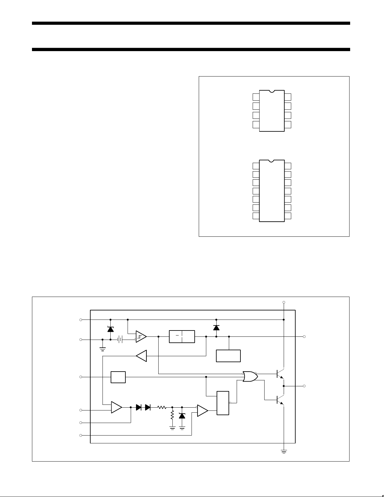
DESCRIPTION
The UC3842 is available in an 8-Pin mini-DIP the necessary
features to implement off-line, fixed-frequency current-mode control
schemes with a minimal external parts count. This technique results
in improved line regulation, enhanced load response characteristics,
and a simpler, easier to design control loop. Topological advantages
include inherent pulse-by-pulse current limiting.
Protection circuitry includes built-in undervoltage lock-out and
current limiting. Other features include fully-latched operation, a 1%
trimmed bandgap reference, and start-up current less than 1mA.
These devices feature a totem-pole output designed to source and
sink high peak current from a capacitive load, such as the gate of a
power MOSFET. Consistent with N-channel power devices, the
output is low in the OFF-state.
FEATURES
•Low start-up current (≤1mA)
•Automatic feed-forward compensation
•Pulse-by-pulse current limiting
•Enhanced load response characteristics
•Undervoltage lock-out with hysteresis
•Double pulse suppression
•High current totem-pole output
•Internally-trimmed bandgap reference
•400kHz operation, guaranteed min
PIN CONFIGURATIONS
N Package
D Package
1
2
3
4 5
6
7
8
1
2
3
4
5
6
7 8
14
13
12
11
10
9
COMP
NC
COMP
V
FB
I
SENSE
RT/C
T
V
FB
I
SENSE
RT/C
T
NC
NC
V
REF
V
CC
OUTPUT
GROUND
NC
V
REF
V
CC
OUTPUT
GROUND
V
C
POWER GROUND
TOP VIEW
TOP VIEW
APPLICATIONS
•Off-line switched mode power supplies
•DC-to-DC converters UC3842
BLOCK DIAGRAM
NOTE:
Pin numbers in parentheses refer to the D package.
(12)7
(9)5
(7)4
(3)2
(1)1
(5)3
7(11)
8(14)
6(10)
5(8)
GND
COMP
CURRENT
SENSE
CURRENT
SENSE
COMPARATOR
PWM
LATCH
INTERNAL
BIAS
5V
REF
UVLO
34V
16V
OSC
ERROR
AMP
+
–
2R
R
1V
2.5V
5.0V
50mA
OUTPUT
6V
V
REF
V
CC
V
FB
S/R
RT/C
T
S
R
Page 2
Philips Semiconductors Linear Products Product specification
UC3842Current-mode PWM controller
August 31, 1994
1101
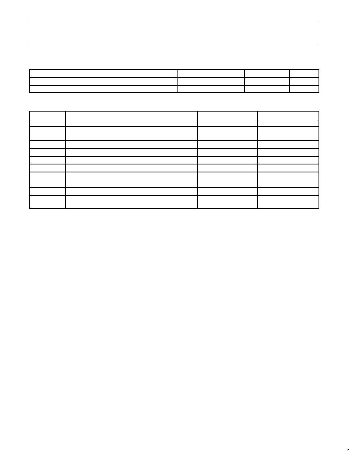
ORDERING INFORMATION
DESCRIPTION TEMPERATURE RANGE ORDER CODE DWG #
8-Pin Plastic Dual In-Line Package (DIP) 0 to +70°C UC3842N 0404B
14-Pin Plastic Small Outline (SO) Package 0 to +70°C UC3842D 0405B
ABSOLUTE MAXIMUM RATINGS
1
SYMBOL
PARAMETER RATING UNIT
V
CC
Supply voltage (ICC<30mA) Self-Limiting
V
CC
Supply voltage
(low impedance source)
30 V
I
OUT
Output current
2, 3
±1 A
Output energy (capacitive load) 5 µJ
Analog inputs (Pin 2, Pin 3) -0.3 to 6.3 V
Error amp output sink current 10 mA
P
D
Power dissipation at TA≤70°C 1 W
(derate 12.5mW/°C for TA>70°C)
2
T
STG
Storage temperature range -65 to +150 °C
T
SOLD
Lead temperature
(soldering, 10sec max)
300 °C
NOTES:
1. All voltages are with respect to Pin 5; all currents are positive into the specified terminal.
2. See section in application note on “Power Dissipation Calculation”.
3. This parameter is guaranteed, but not 100% tested in production.
Page 3

Philips Semiconductors Linear Products Product specification
UC3842Current-mode PWM controller
August 31, 1994
1102
DC AND AC ELECTRICAL CHARACTERISTICS
0≤TJ≤70°C for UC3842; VCC=15V; RT=10kW; CT=3.3nF, unless otherwise specified.
UC3842
SYMBOL
PARAMETER
TEST CONDITIONS
Min Typ Max
UNIT
Reference section
V
OUT
Output voltage TJ=25°C, IO=1mA 4.90 5.00 5.10 V
Line regulation 12≤VIN≤25V 6 20 mV
Load regulation 1≤IO≤20mA 6 25 mV
Temp. stability
1
0.2 0.4 mV/°C
Total output variation
1
Line, load, temp. 4.82 5.18 V
V
NOISE
Output noise voltage
1
10Hz≤f≤10kHz, TJ=25°C 50 µV
Long-term stability
1
TJ=125°C, 1000 Hrs. 5 25 mV
Output short-circuit TJ=25 -30 -100 -130 mA
Output short-circuit -55<TJ≤0°C -30 -100 -180 mA
Oscillator section
Initial accuracy TJ=25°C 47 52 57 kHz
Voltage stability 12≤VCC≤25V 0.2 1 %
Temp. stability
1
T
MIN≤TJ≤TMAX
5 %
Amplitude V
PIN 4
peak-to-peak 1.7 V
Error amp section
Input voltage V Pin 1=2.5V 2.42 2.50 2.58 V
I
BIAS
Input bias current -0.3 -2 µA
A
VOL
2≤VO≤4V 65 90 dB
Unity gain bandwidth
1
TJ=25°C 0.7 1 MHz
Unity gain bandwidth T
MIN<TJ<TMAX
0.5 MHz
PSRR Power supply rejection ratio 12≤VCC≤25V 60 70 dB
I
SINK
Output sink current V
PIN 2
=2.7V, V
PIN 1
=1.1V 2 6 mA
I
SOURCE
Output source current V
PIN 2
=2.3V, V
PIN 1
=5V -0.5 -0.8 mA
V
OUT
High V
PIN 2
=2.3V, RL=15k to ground 5 6 V
V
OUT
Low V
PIN 2
=2.7V, RL=15k to Pin 8 0.7 1.1 V
Current sense section
Gain
2, 3
2.85 3 3.15 V/V
Maximum input signal
2
V
PIN 1
=5V 0.9 1 1.1 V
PSRR Power supply rejection ratio
2
12≤VCC≤25V 70 dB
I
BIAS
Input bias current -2 -10 µA
Delay to output
1
150 300 ns
Page 4

Philips Semiconductors Linear Products Product specification
UC3842Current-mode PWM controller
August 31, 1994
1103
DC AND AC ELECTRICAL CHARACTERISTICS
0≤TJ≤70°C for UC3842; VCC=154; RT=10kΩ; CT=3.3nF, unless otherwise specified
UC3842
SYMBOL
PARAMETER
TEST CONDITIONS
Min Typ Max
UNIT
Output section
I
SINK
=20mA 0.1 0.4
VOLOutput Low-Level
I
SINK
=200mA 1.5 2.2
V
I
SOURCE
=20mA 13 13.5
VOHOutput High-Level
I
SOURCE
=200mA 12 13.5
V
t
R
Rise time CL=1nF 50 150 ns
t
F
Fall time CL=1nF 50 150 ns
Undervoltage lockout section
Start threshold 14.5 16 17.5 V
Min. operating voltage after turn on 8.5 10 11.5 V
PWM section
Maximum duty cycle 93 97 100
Minimum duty cycle 0
%
Total standby current
Start-up current 0.5 1 mA
I
CC
Operating supply current V
PIN 2=VPIN 3
=0V 11 17 mA
VCC zener voltage ICC=25mA 34 V
Maximum operating frequency section
Maximum operating frequency for all
functions operating cycle-by-cycle
400 kHz
NOTES:
1. These parameters, although guaranteed, are not 100% tested in production.
2. Parameter measured at trip point of latch with V
PIN 2
=0.
3. Gain defined as:
A
V
PIN
1
V
PIN
3
; 0 V
PIN
3
0.8V
UNDERVOLTAGE LOCKOUT
UC3842
V
ON
16V
V
OFF
10V
NOTE:
During Undervoltage Lock-Out, the output driver is biased to a high
impedance state. Pin 6 should be shunted to ground with a bleeder
resistor to prevent activating the power switch with output leakage current.
7
V
CC
ON/OFF COMMAND
TO REST OF IC
V
CC
V
OFFVON
I
CC
<15mA
<1mA
ERROR AMP CONFIGURATION
NOTE:
Error AMP can source or sink up to 0.5mA.
2.5V
0.5mA
2
1
COMP
V
FB
Z
I
+
–
Page 5

Philips Semiconductors Linear Products Product specification
UC3842Current-mode PWM controller
August 31, 1994
1104
CURRENT SENSE CIRCUIT
NOTE:
Peak current (I
S
) is determined by the formula:
A small RC filter may be required to suppress switch transients.
ISMAX
1.0V
R
s
R
2R
1V
ERROR
AMP
CURRENT
SENSE
COMPARATOR
COMP
CURRENT
SENSE
GND
R
R
S
I
S
1
3
5
TYPICAL PERFORMANCE CHARACTERISTICS
Output Saturation Characteristics
Error Amplifier Open-Loop
Frequency Response
VOLTAGE GAIN (dB)
FREQUENCY (Hz)
PHASE (DEG)
100
80
60
40
20
0
–20
10 100 1k 10k 100k 1M 10M
45
0
–45
–90
–135
–180
–225
SATURATION VOLTAGE (V)
4
3
2
1
0
0.01 0.03 0.05 0.1 0.3 0.5 1.0
OUTPUT CURRENT, SOURCE OR SINK (A)
0
Av
Page 6

Philips Semiconductors Linear Products Product specification
UC3842Current-mode PWM controller
August 31, 1994
1105
OPEN-LOOP LABORATORY TEST FIXTURE
NOTE:
High peak currents associated with capacitive loads necessitate careful grounding techniques. Timing and bypass capacitors should be connected close to Pin 5 in a single point
ground. The transistor and 5k potentiometer are used to sample the oscillator waveform and apply an adjustable ramp to Pin 3.
4.7k
ERROR AMP
ADJUST
4.7k
2N2222
100k
5k
ADJUST
COMP
1
2
3
4
8
7
6
5
OUTPUT
GND
1k
1W
OUTPUT
GND
V
REF
V
CC
R
T
UC3842
V
FB
I
SENSE
RT/C
T
V
REF
V
CC
0.1µF
I
SENSE
C
T
A
0.1µF
SHUTDOWN TECHNIQUES
NOTE:
Shutdown of the UC3842 can be accomplished by two methods; either raise Pin 3 above 1V or pull Pin 1 below a voltage two diode drops above ground. Either method causes the
output of the PWM comparator to be high (refer to Block Diagram). The PWM latch is reset dominant so that the output will remain low until the next clock cycle after the shutdown
condition at Pins 1 and/or 3 is removed. In the examples shown, an externally-latched shutdown may be accomplished by adding an SCR which will be reset by cycling
VCC below the lower UVLO threshold (10V). At this point all internal bias is removed, allowing the SCR to reset.
1
COMP
SHUTDOWN
TO CURRENT
SHUTDOWN
SENSE RESISTOR
4.7k
4.7k
8
3
500
I
SENSE
Page 7

Philips Semiconductors Linear Products Product specification
UC3842Current-mode PWM controller
August 31, 1994
1106
OFF-LINE FLYBACK REGULATOR
UC3842
4.7 1W
673-3
AC
INPUT
250V
56k
1W
16V
20k
150k
3.6k
100pF
COMP
10k
2
1
8
4
7
6
3
5
GND
CUR
SEN
OUT
27
20k
1k
0.85
UFN432
1N3613
1N3613
ISOLATION
BOUNDARY
2.5k
820pF
1N3613
400V
4.7k
4W
T1
USD735
10V
DC
OUT
(5V 2–5A)
+
–
220µF
10µF
20V
0.01µF
0.01µF
0.0047µF
0.01µF
4700µF
470pF
V
FB
V
REF
RT/C
T
V
CC
NOTES:
T1: Coilcraft E-4140-B
Primary – 97 turns
single AWG24
Secondary – 4 turns
4 parallel
AWG22
control – 9 turns
–3 parallel AWG28
SPECIFICATIONS
Input line voltage: 90VAC to 130V
AC
Input frequency: 50 or 60Hz
Switching frequency: 40kHz±10%
Output power: 25W maximum
Output voltage: 5V±5%
Output current: 2 to 5A
Line regulation: 0.01%/V
Load regulation: 8%/A
*
Efficiency @ 25 W,
V
IN
=90VAC: 70%
V
IN
=130VAC: 65%
Output short-circuit current: 2.5A average
NOTE:
This circuit uses a low-cost feedback scheme in which the DC
voltage developed from the primary-side control winding is sensed
by the UC3842 error amplifier. Load regulation is therefore
dependent on the coupling between secondary and control
windings, and on transformer leakage inductance. For applications
requiring better load regulation, a UC1901 Isolated Feedback
Generator can be used to directly sense the output voltage.
Page 8

Philips Semiconductors Linear Products Product specification
UC3842Current-mode PWM controller
August 31, 1994
1107
SYNCHRONIZATION AND MAXIMUM DUTY CYCLE CLAMP
NOTES:
f +
1.44
(RA) 2RB) C
D
MAX
+
R
B
RA) 2R
B
5V
4
8
7
2
6
1
3
GND
OUT
RESET
DISCH
TRIG
THRESH
NE555
7
UC3842
TO OTHER
UC3842s
4
5
GND
V
CC
R
A
R
B
C
V
CC
RT/C
T
 Loading...