

Page 1
4/97
• Full-Step, Half-Step and Micro-Step
Capability
• Bipolar Output Current up to 1A
• Wide Range of Motor Supply Voltage
10-46V
• Low Saturation Voltage with Integrated
Bootstrap
• Built-In Fast Recovery Commutating
Diodes
• Current Levels Selected in Steps or Varied
Continuously
• Thermal Protection with Soft Intervention
Stepper Motor Drive Circuit
The UC3717A is an impro ved ver sion of the UC3717, us ed to switch
drive the current in one winding of a bipolar stepper motor. The
UC3717A has been modified to supply higher winding current, more
reliable thermal protection, and improved efficiency by providing integrated boots trap circuitry to lower recirculation saturation voltages.
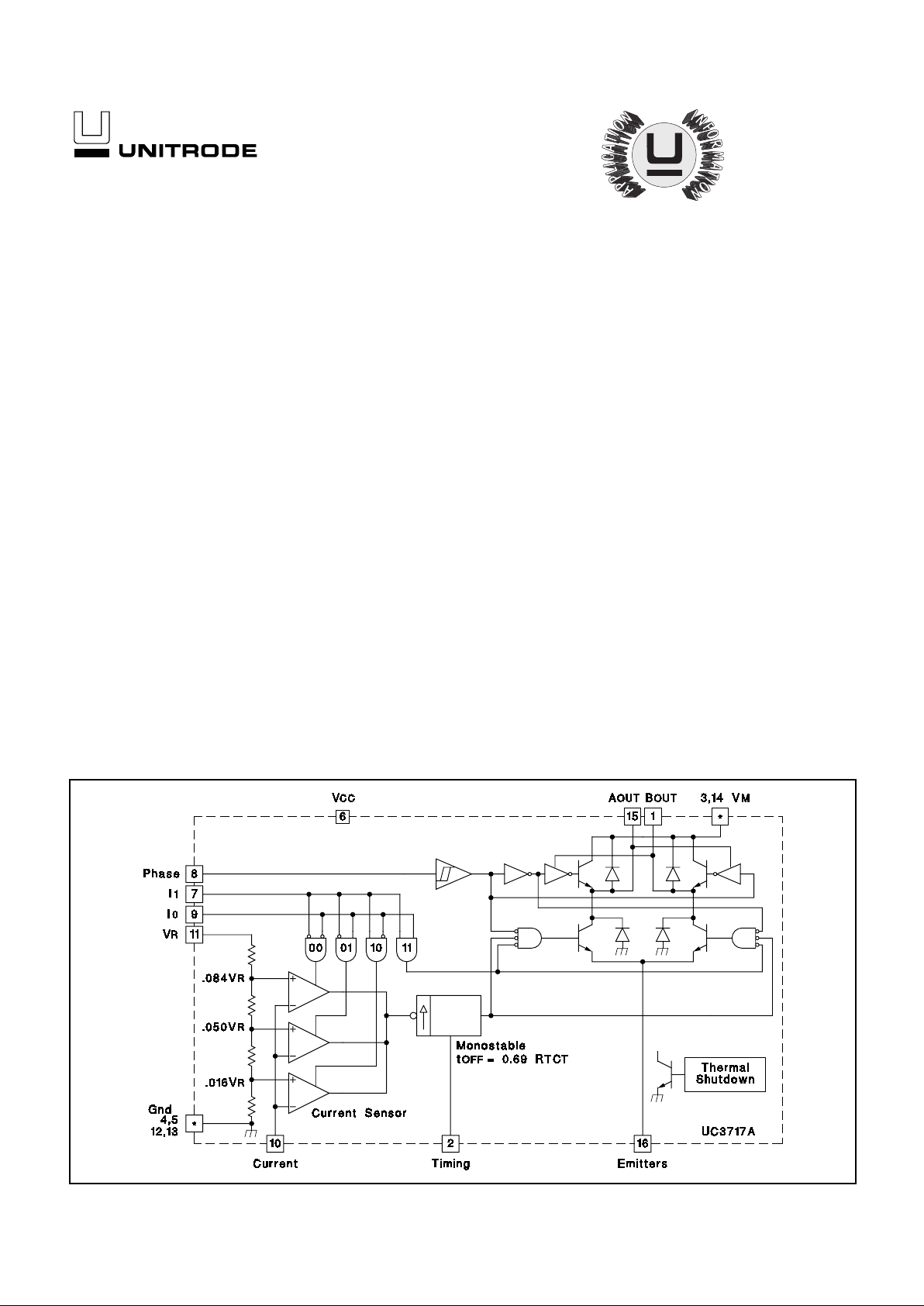
The diagram shown below presents the building blocks of the
UC3717A. Includ ed are an LS-TTL compatible l ogic input, a current
sensor, a monostable, a ther mal s hutd ow n netw ork, and an H -bridge
output stage. The output stage features built-in fast recovery commutating diodes and integrated bootstrap pull up. Two UC3717As
and a few external components form a complete control and drive
unit for LS-TTL or micro-processor controlled stepper motor systems.
The UC3717A is characterized for operation over the temperature
range of 0°C to +70°C.
UC3717A
BLOCK DIAGRAM
FEATURES DESCRIPTION
Voltage
Logic Supply, VCC. . . . . . . . . . . . . . . . . . . . . . . . . . . . . . . . . . . . . . 7V
Output Supply, Vm. . . . . . . . . . . . . . . . . . . . . . . . . . . . . . . . . . . . . 50V
Input Voltage
Logic Inputs (Pins 7, 8, 9) . . . . . . . . . . . . . . . . . . . . . . . . . . . . . . . . 6V
Analog Input (Pin 10). . . . . . . . . . . . . . . . . . . . . . . . . . . . . . . . . . . V
CC
Reference Input (Pin 11) . . . . . . . . . . . . . . . . . . . . . . . . . . . . . . . . 15V
Input Current
Logic Inputs (Pins 7, 8, 9) . . . . . . . . . . . . . . . . . . . . . . . . . . . . . -10mA
Analog Inputs (Pins 10, 11). . . . . . . . . . . . . . . . . . . . . . . . . . . . -10mA
Output Current (Pins 1, 15) . . . . . . . . . . . . . . . . . . . . . . . . . . . . . . . ±1.2A
Junction Temperature, TJ. . . . . . . . . . . . . . . . . . . . . . . . . . . . . . . +150°C
Storage Temperature Range, TS. . . . . . . . . . . . . . . . . . -55°C to +150°C
ABSOLUTE MAXIMUM RATINGS (Note 1)
Note 1: All voltages are with respect to ground, Pins 4,
5, 12, 13. Currents are positive into, negative out of the
specified terminal. Pin numbers refer to DIL-16 package.
Consult Packaging Section of Databook for thermal limitations and considerations of package.
1
Page 2
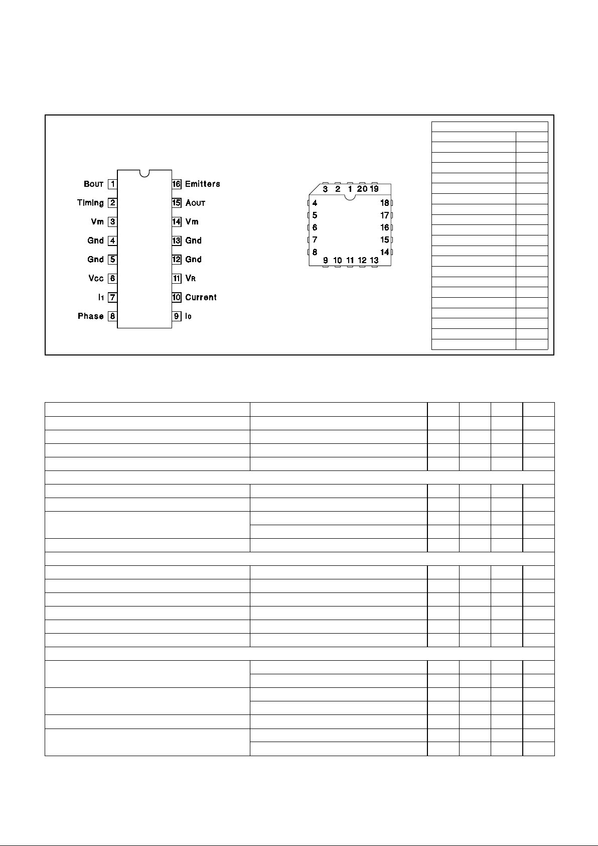
UC3717A
PLCC-20 (TOP VIEW)
Q Package
PACKAGE PIN FUNCTION
FUNCTION PIN
N/C
1
B
OUT
2
Timing
3
V
m
4
Gnd
5
N/C
6
Gnd
7
V
CC
8
I
1
9
Phase
10
N/C
11
I
0
12
Current
13
V
R
14
Gnd
15
N/C
16
Gnd
17
V
m
18
A
OUT
19
Emitters
20
DIL-16 (TOP VIEW)
J or N Package
CONNECTION DIAGRAMS
ELECTRICAL CHARACTERISTICS
(Refer to the te st c ircui t, Figure 6. Vm = 36V, VCC = 5V, VR = 5V, TA = 0°C to 70°C,
unless otherwis e stat ed , TA = TJ.)
PARAMETERS TEST CONDITIONS MIN TYP MAX UNITS
Supply Voltage, Vm (Pins 3, 14) 10 46 V
Logic Supply Voltage, V
CC
(Pin 6) 4.75 5.25 V
Logic Supply Current, I
CC
(Pin 6) IO = I1 = 0 7 15 mA
Thermal Shutdown Temperature +160 +180 °C
Logic Inputs
Input Low Voltage, (Pins 7, 8, 9) 0.8 V
Input High Voltage, (Pins 7, 8, 9) 2 V
CC
V
Low Voltage Input Current, (Pins 7, 8, 9) V
I
= 0.4V, Pin 8 -100
µ
A
V
I
= 0.4V, Pins 7 and 9 -400 mA
High Voltage Input Current, (Pins 7, 8, 9) V
I
= 2.4V 10
µ
A
Comparators
Comparator Low, Thres ho ld Volt ag e (Pin 10) V
R
= 5V; IO = L; I1 = H 668090mV
Comparator Medium, Threshold Voltage (Pin 10) V
R
= 5V; IO = H; I1 = L 236 250 266 mV
Comparator High, Thre sh ol d Vol ta ge (Pin 10 ) V
R
= 5V; IO = L; I1 = L 396 420 436 mV
Comparator Input, Current (Pin 10)
±
20
µ
A
Cutoff Time, t
OFF
RT = 56kΩ, CT = 820pF 25 35
µ
s
Turn Off Delay, t
D
(See Figure 5) 2
µ
s
Source Diode-Transistor Pair
Saturation Voltage, V
SAT
(Pins 1, 15) Im = -0.5A, Conduction Period 1.7 2.1 V
(See Figure 5) I
m
= -0.5A, Recirculation Period 1.1 1.35 V
Saturation Voltage, V
SAT
(Pins 1, 15) Im = -1A, Conduction Period 2.1 2.8 V
(See Figure 5) I
m
= -1A, Recirculation Period 1.7 2.5 V
Leakage Current V
m
= 40V 300
µ
A
Diode Forward Voltage, V
F
Im = -0.5A 1 1.25 V
I
m
= -1A 1.3 1.7 V
2
Page 3
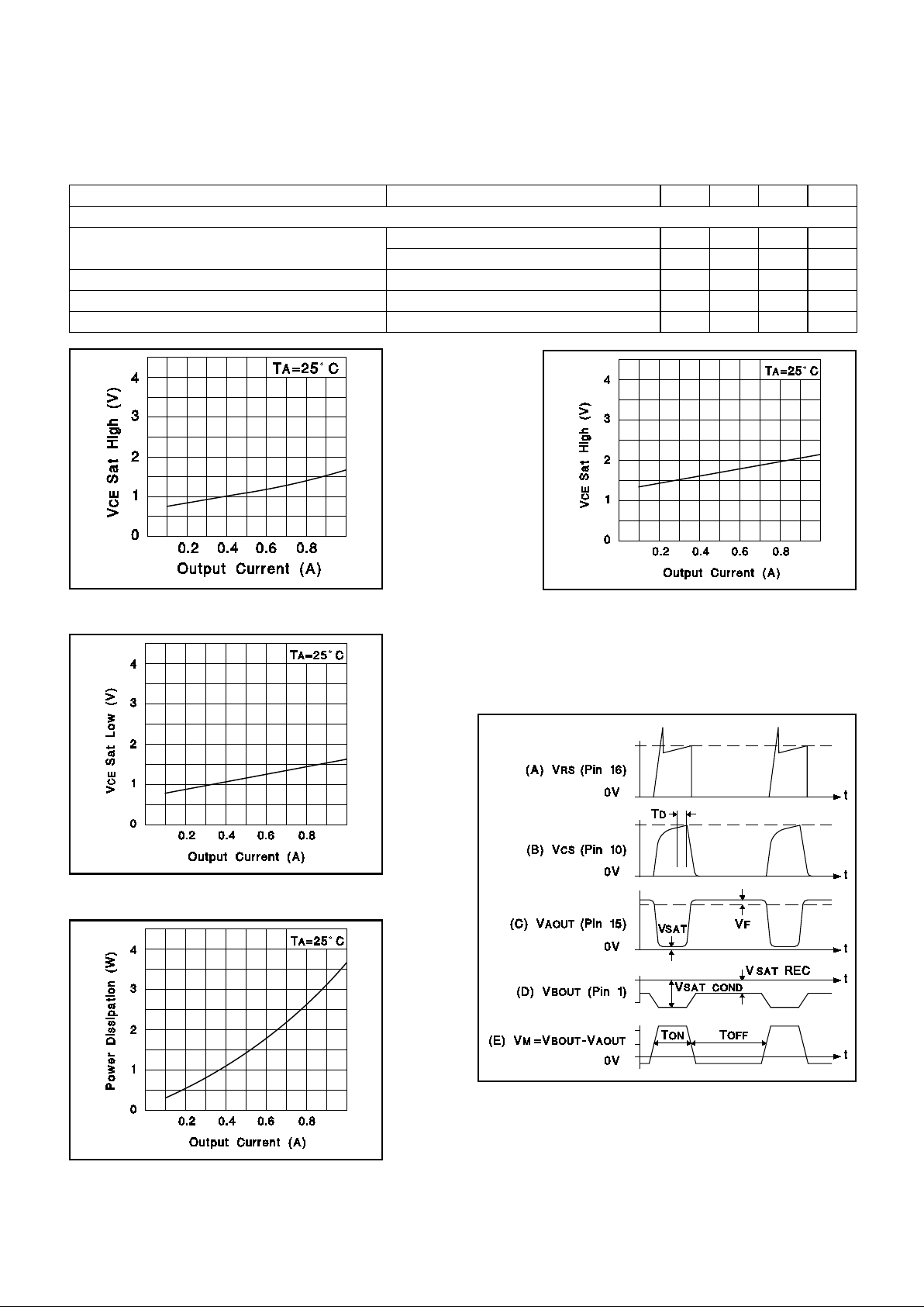
Figure 1. Typical Source Saturation Voltage
vs Output Current (Recirculation Period)
Figure 2. Typical Source Saturation Voltage
vs Output Current (Conduction Period)
UC3717A
PARAMETERS TEST CONDITIONS MIN TYP MAX UNITS
Sink Diode-Transistor Pair
Saturation Voltage, V
SAT
(Pins 1, 15) Im = 0.5A 0.8 1.1 1.35 V
I
m
= 1A 1.6 2.3 V
Leakage Current V
m
= 40V 300
µ
A
Diode Forward Voltage, V
F
Im = 0.5A 1.1 1.5 V
I
m
= 1A 1.4 2 V
ELECTRICAL
CHARACTERISTICS (cont.)
(Refer to the te st c ircui t, Figure 6. VM = 36V, VCC = 5V, VR = 5V, TA = 0°C to 70°C, unless
otherwise stated, TA = TJ.)
Figure 3. Typical Sink Saturation
Voltage vs Output Current
Figure 4. Typical Power Dissipation
vs Output Current
Figure 5. Typical Waveforms with MA Regulating
(phase = 0)
3
Page 4

The UC3717A’s drive circuit shown in the block diagram
includes the following components.
(1) H-bridge output stage
(2) Phase polarity logic
(3) Voltage divider coupled with current sensing compa rators
(4) Two-bit D/A current level select
(5) Monostable generating fixed off-time
(6) Thermal protection
OUTPUT STAGE
The UC3717A’s output stage consists of four Darlington
power trans i stors and assoc i a te d re c i r cul a ti n g power di odes in a full H-bridge configuration as shown in Figure
7. Also presented, is the new added feature of inte-
grated bootstrap pull up, which improves device performance during switched mode operation. While in
switched mode, with a low level phase polarity input, Q2
is on and Q3 is being switched. At the moment Q3 turns
off, winding current begins to decay through the commutating diod e pu lling the collector of Q3 above the supply
voltage. Meanwhile, Q6 turns on pulling the base of Q2
higher than its previ ous val ue. The net effect lowers the
saturation voltage of source transistor Q2 during recirculation, thus improving efficiency by reducing power dissipation.
UC3717A
Figure 6. UC3717A Test Circuit
Figure 7. Simplified Schematic of Output Stage
Note: Dashed lines indic ate current decay path s.
FUNCTIONAL DESCRIPTION
4
Page 5

PHASE POLARITY INPUT
The UC3717A phase polarity input controls current direction in the motor winding. Built-in hysteresis insures immunity to noise, something frequently present in
switched drive environments. A low level phase polarity
input enables Q 2 and Q3 as shown in Figure 7. During
phase revers al, the acti ve transist ors are both turned off
while winding current delays through the commutating diodes shown. As winding current decays to zero, the inactive transistors Q1 and Q4 turn on and charge the
winding with current of the reverse direction. This delay
insures noi se immunity a nd freedom from power supply
current spikes caused by overlapping drive signals.
PHASE INPUT Q1, Q4 Q2, Q3
LOW OFF ON
HIGH ON OFF
CURRENT CONTROL
The voltage div ider, comparators, monostable, and twobit D/A provide a me ans to sen se winding pe ak current,
select win di n g peak cur rent, and disabl e the windi ng si nk
transistors.
The UC3717A switched driver accomplishes current control using an algorithm referred to as "fixed off-time."
When a vol tage is applied across the motor winding, the
current through the winding increases exponentially. The
current can be sensed across an external resistor as an
analog voltage proportional to instantaneous current.
This voltage is normally filtered with a simple R
C
lowpass network to remove high frequency transients, and
then compared to one of the thr ee selectable threshol ds.
The two bit D/A input sign al dete rmin es wh ich on e of the
three thres holds is selected, correspondi ng to a desired
winding peak current level. At the moment the sense voltage rises above the selected threshold, the UC3717A’s
monostable is triggered and disables both output sink
drivers fo r a fixed o ff-time. The w inding current then circulates th rough t he sourc e transistor and appropriate diode. The refe rence termin al of the UC3717A provides a
means of conti nuously adj usting th e current threshold to
allow microstepping. Table 1 presents the relationship
between the t wo-bit D/A input signa l and selectable current level.
TABLE 1
I
O
I
1
CURRENT LEVEL
0 0 100%
10 60%
01 19%
1 1 Current Inhibit
OVERLOAD PROTECTION
The UC3717A is equipped with a new, more reliable thermal shutdown circuit which limits the junction tempera-
ture to a maximum of 180C by reducing the windi ng current.
PERFORMANCE CONSIDERATIONS
In order to achieve optimum performance from the
UC3717A careful atten tion s houl d be given to the following items.
External Components:
The UC3717A requires a minimal number of ex ternal compone nts to form a complete
control and switch drive unit. However, proper selection
of external components is necessary for optimum performance. The timing pin, (pin 2) is normal ly connected
to an RC network which sets the off-time for the sink
power trans istor during switc hed mode. As shown i n Figure 8, prior to switched mode, the winding current increases exponentially to a peak value. Once peak
current is attained the monostable is triggered which
turns off the lo wer sink drivers for a fixed off-time. During
off-time windi ng current decays th rough the appropriate
diode and sou rce transistor. The moment off-time times
out, the motor current agai n rises exponentially producing the ripple waveform shown. The mag nitude of winding ripple is a direct function of off-time. For a given
off-time T
OFF
, the values of RT and CT can be calculated
from the expression:
T
OFF
=
0.69
RTC
T
with the re strict ion that RT should be in the rang e of 10100k. As s h ow n i n Fi gu r e 5, t he s witc h frequency F
S
is a
function of T
OFF
and TON. Since TON is a function of the
reference voltage, sense resistor, motor supply, and
winding e lectrical cha racteristics, it generally v aries during different modes of operation. Thus, F
S
may be ap-
proximated nominally as:
F
S
=
1
⁄
1.5
(
T
OFF
).
Normally, Switch Frequency Is Selected Greater than
Figure 8. A typical winding current waveform. Winding current rises exponentially to a selected peak
value. The peak value is limited by switched mode
operation producing a ripple in winding current. A
phase polarity reversal command is given and winding current decays to zero, then increases exponentially.
UC3717A
FUNCTIONAL DESCRIPTION (cont.)
5
Page 6

Low-pass filter components RC CC should be selected so
that all switching transients from the power transistors
and commutating diodes are well smoothed, but the primary signal, which can be in the range of 1/T
OFF
or
higher must be passed. Figure 5A shows the waveform
which must be smoothed, Figure 5B presents the desired
waveform that just smoothes out overshoot without radical distortion.
The sense resistor should be chosen as small as practical to allo w as much of the winding supply voltage to be
used as overd rive to the motor winding. V
RS
, the voltage
across the sense resistor, should not exceed 1.5V.
Voltage Overdrive:
In many applications, maximum
speed or step rate is a desirable performance characteristic. Maximum step rate is a direct function of the time
necessary to reverse w inding current with each step. In
response to a constant motor supply voltage, the winding
current chan ges exponentially with time, whos e shape is
determined b y the windi ng time constant and expressed
as:
I
m
=
V
m
R [1−EXP
(
−
R
T
⁄
L
)
]
as present ed in Figure 9 . Wit h rated v oltage applied, the
time required to reach rated current is excessive when
compared with the time required with over-voltage applied, even th ough the time constant L/R remains constant. With over-voltage however, the final value of
current is excessive and must be prevented. This is accomplishe d w ith s wit ch driv e by repetitivel y switc hing the
sink drivers on and off, so as to maintain an average
value of current equal to the rated value. This results in a
small amount of rippl e in the controlled current, but the
increase in s tep rate and pe rformance may be considerable.
Interference:
Electrical noise generated by the c hopping
action can cause interference problems, particularly in
the vicinity of magnetic storage media. With this in mind,
printed ci rcuit layouts, wire runs and dec oupling must be
considered. 0.01 to 0.1µF ceramic capacitors for high frequency bypass located near the drive package across
V+ and ground might be very helpful. The connection
and ground leads of the current sensing components
should be kept as short as possible.
Half-Stepping:
In half step seq uence the power input to
the motor alt ernates between one or two phases being
energized. In a two phase motor the electrical phase shift
between the windings is 90°. The torque developed is the
vector sum of the two windings energized. Therefore
when only one winding is energized the torque of the motor is reduced by approximately 30%. This causes a
torque ripple and if it is necessary to compensate for this,
the V
R
input can be used to boost the current of the sin-
gle energized winding.
Figure 9. With rated volt age applied, winding current does not exceed rated value, but takes L/R seconds to
reach 63% of its final value - probably too long. Increased performance requires an increase in applied voltage, of overdrive, and therefore a m eans to limit current. The UC3717A motor driver performs this task efficiently.
UC3717A
FUNCTIONAL DESCRIPTION (cont.)
6
Page 7

UC3717A
The θJA of the UC3717AN plastic package can be reduced by soldering the GND pins to a suitable copper
area of the printed circuit board or to an external heat
sink. Due to different lead frame design, θ
JA
of the ceramic J package cannot be similarly reduced.
The diagram of Figure 11 shows the maximum package
power P
TOT
and the θJA as a function of the side " l " of
two equal square copper areas having a thickness of 35µ
(see Figure 10).
During soldering the pins’ temperature must not exceed
260°C and t he s o l de r ing time must not be longer than 12
seconds.
The printed circuit copper area must be connected to
electrical ground.
APPLICATIONS
A typical chopper drive for a two phase bipolar permanent magnet or hybrid stepping motor is shown in Figure
12. The input can be controlled by a microprocessor,
TTL, LS, or CMOS logic.
The timing diag ram in Fig ure 13 sho ws the required signal input for a two phase, full step stepping sequence.
Figure 14 shows the required input signal for a one
phase-two phase stepping sequence called half-stepping.
The circuit of Figure 15 provides the signal shown i n Figure 13, and in conjunction with the circuit shown in Figure 12 will implement a pulse-to-step two phase, full
step, bi-directional motor drive.
The schemati c of Figure 16 shows a pulse to half step
circuit generating the signal shown in Figure 14. Care
has been taken to change the phase signal the same
time the cur rent inhi bit is a pplied . This will allow the cur rent to decay faster and therefore enhance the motor
performance at high step rates.
Figure 10. Example of P.C. Board Copper
Area which is used as Heatsink.
MOUNTING INSTRUCTIONS
Figure 12. Typical Chopper Drive for a Two
Phase Permanent Magnet Motor.
Figure 11. Maximum Package Power and Junction
to Ambient Thermal Resistance vs Side "
l
".
7
Page 8

Figure 16. Half-Step, Bi-directional Drive Logic
Figure 14. Phase and Current-Inhibit Signal for Half-Steppin g (8 Step Sequence)
Figure 15. Full Step, Bi-directional Two Phase Drive Logic
UC3717A
UNITRODE CORPORATI ON
7 CONTINENTAL BLVD. • MERRIMACK, NH 03054
TEL. (603) 424- 24 10 • FAX (603) 424-3460
Figure 13. Phase Input Signal for Two Phase Full Step Drive (4 Step Sequence)
8
Page 9

IMPORTANT NOTICE
T exas Instruments and its subsidiaries (TI) reserve the right to make changes to their products or to discontinue
any product or service without notice, and advise customers to obtain the latest version of relevant information
to verify, before placing orders, that information being relied on is current and complete. All products are sold
subject to the terms and conditions of sale supplied at the time of order acknowledgement, including those
pertaining to warranty, patent infringement, and limitation of liability.
TI warrants performance of its semiconductor products to the specifications applicable at the time of sale in
accordance with TI’s standard warranty. Testing and other quality control techniques are utilized to the extent
TI deems necessary to support this warranty. Specific testing of all parameters of each device is not necessarily
performed, except those mandated by government requirements.
CERT AIN APPLICATIONS USING SEMICONDUCTOR PRODUCTS MA Y INVOLVE POTENTIAL RISKS OF
DEATH, PERSONAL INJURY, OR SEVERE PROPERTY OR ENVIRONMENTAL DAMAGE (“CRITICAL
APPLICATIONS”). TI SEMICONDUCTOR PRODUCTS ARE NOT DESIGNED, AUTHORIZED, OR
WARRANTED TO BE SUITABLE FOR USE IN LIFE-SUPPORT DEVICES OR SYSTEMS OR OTHER
CRITICAL APPLICATIONS. INCLUSION OF TI PRODUCTS IN SUCH APPLICA TIONS IS UNDERSTOOD T O
BE FULLY AT THE CUSTOMER’S RISK.
In order to minimize risks associated with the customer’s applications, adequate design and operating
safeguards must be provided by the customer to minimize inherent or procedural hazards.
TI assumes no liability for applications assistance or customer product design. TI does not warrant or represent
that any license, either express or implied, is granted under any patent right, copyright, mask work right, or other
intellectual property right of TI covering or relating to any combination, machine, or process in which such
semiconductor products or services might be or are used. TI’s publication of information regarding any third
party’s products or services does not constitute TI’s approval, warranty or endorsement thereof.
Copyright 1999, Texas Instruments Incorporated
 Loading...