

Page 1
查询UC2706供应商
Dual Output Driver
UC1706
UC2706
UC3706
FEATURES
• Dual, 1.5A Totem Pole Outputs
• 40nsec Rise and Fall into 1000pF
• Parallel or Push-Pull Operation
• Single-Ended to Push-Pull Conversion
• High-Speed, Power MOSFET
Compatible
• Low Cross-Conduction Current Spike
• Analog, Latched Shutdown
• Internal Deadband Inhibit Circuit
• Low Quiescent Current
• 5 to 40V Operation
• Thermal Shutdown Protection
• 16-Pin Dual-In-Line Package
• 20-Pin Surface Mount Package
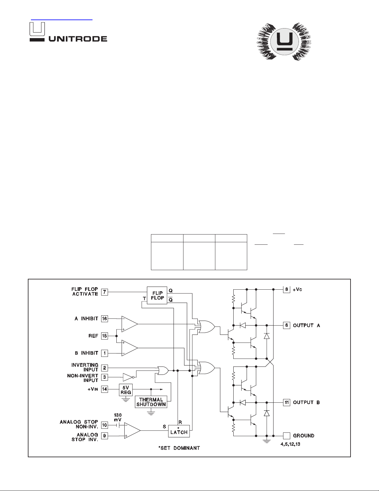
BLOCK DIAGRAM
DESCRIPTION
The UC1706 family of output drivers are made with a high-speed
Schottky process to interface between low-level control functions and
high-power switching devices - particularly power MOSFET's. These devices implement three generalized functions as outlined below.
First: They accept a single-ended, low-current digital input of either polarity and process it to activate a pair of high-current, totem pole outputs
which can source or sink up to 1.5A each.
Second: They provide an optional single-ended to push-pull conversion
through the use of an internal flip-flop driven by double-pulsesuppression logic. With the flip-flop disabled, the outputs work in parallel
for 3.0A capability.
Third: Protection functions are also included for pulse-by-pulse current
limiting, automatic deadband control, and thermal shutdown.
These devices are available in a two-watt plastic “bat-wing” DIP for operation over a 0°C to 70°C temperature range and, with reduced power,
in a hermetically sealed cerdip for -55°C to +125°C operation. Also available in surface mount Q and L packages.
TRUTH TABLE
INV N.I OUT
H
L
H
L
H
H
L
L
L
H
L
L
OUT = INV and N.I.
OUT
= INV or N.I.
10/98
Page 2
ABSOLUTE MAXIMUM RATINGS
....................................... N--Pkg ............ J--Pkg
Supply Voltage, VIN .........................40V..................40V
Collector Supply Voltage, VC ..................40V..................40V
Output Current (Each Output, Source or Sink)
Steady--State..........................±500mA ..............±500mA
Peak Transient..........................±1.5A ................±1.0A
Capacitive Discharge Energy .............. 20mJ................. 15mJ
Digital Inputs ..............................5.5V .................5.5V
Analog Stop Inputs......................... VIN.................. VIN
Power Dissipation at TA = 25°C (See Note) .......2W ..................1W
Power Dissipation at T (Leads/Case) = 25°C......5W...................2
(See Note)
Operating Temperature Range ......................--55°C to +125°C
Storage Temperature Range........................--65°C to +150°C
Lead Temperature (Soldering, 10 Seconds) ................300°C
Note: All voltages are with respect to the four ground pins which must be connected
together.All currents are positive into, negative out of the specified trerminal. Consult
Packaging sections of the Databook for thermal limitations and considerations of package.
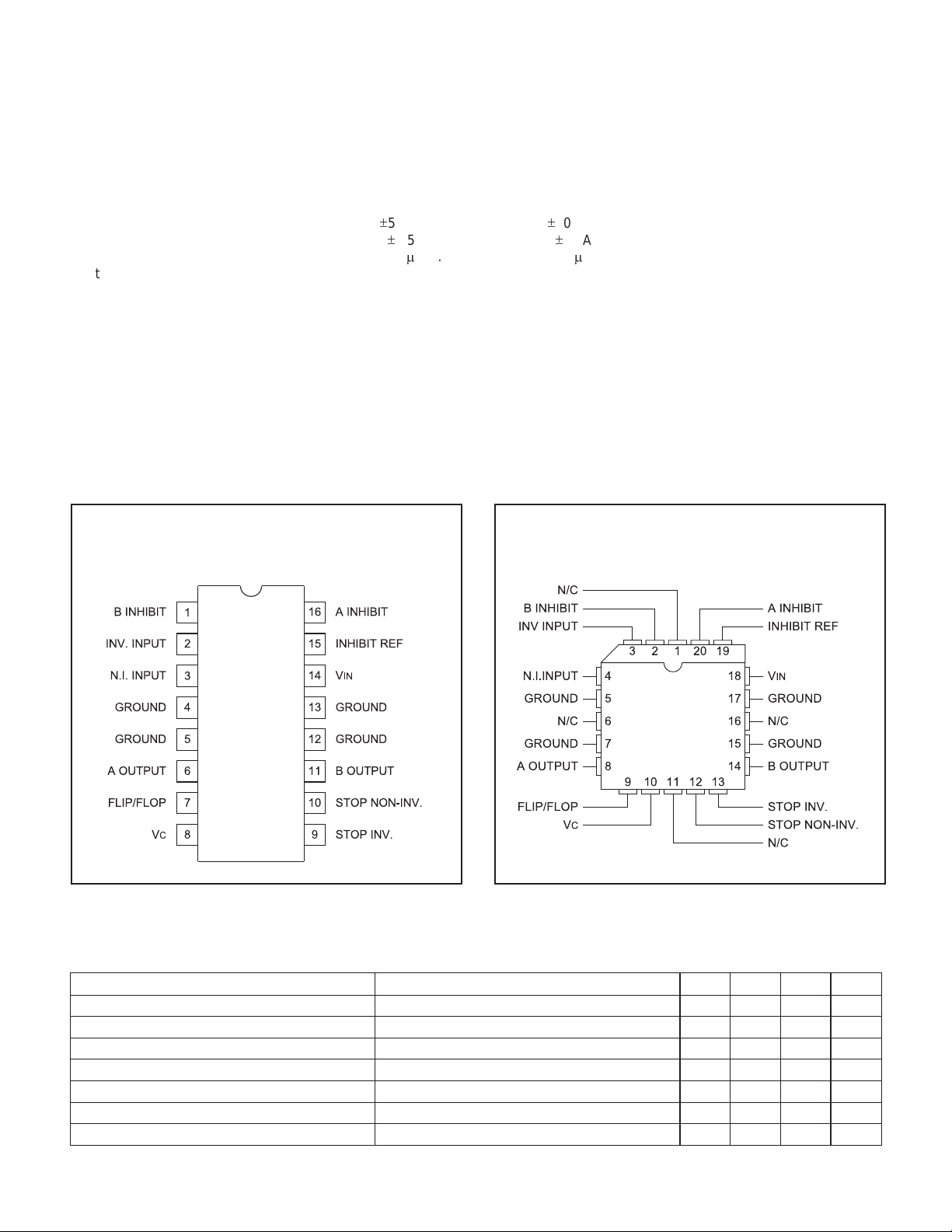
CONNECTION DIAGRAMS
UC1706
UC2706
UC3706
DIL-16, SOIC-16 (TOP VIEW)
JorNPackage,DWPackage
Note: All four ground pins must be connected to a common
ground.
PLCC-20, LCC-20 (TOP VIEW)
Q, L Packages
ELECTRICAL CHARACTERISTICS: Unless otherwise stated, these specifications apply for TA = –55°C to +125°C for
the UC1706, –25°C to +85°C for the UC2706 and 0°C to +70°C for the UC3706; VIN =VC= 20V. TA =TJ.
PARAMETERS TEST CONDITIONS MIN TYP MAX UNITS
IN Supply Current VIN = 40V 8 10 mA
V
VC Supply Current VC = 40V, Outputs Low 4 5 mA
VC Leakage Current VIN =0,VC= 30V, No Load .05 0.1 mA
Digital Input Low Level 0.8 V
Digital Input High Level 2.2 V
Input Current V
Input Leakage V
I = 0 –0.6 –1.0 mA
I = 5V .05 0.1 mA
2
Page 3

UC1706
UC2706
UC3706
ELECTRICAL CHARACTERISTICS: Unless otherwise stated, these specifications apply for TA = –55°C to +125°C for
the UC1706, –25°C to +85°C for the UC2706 and 0°C to +70°C for the UC3706; VIN =VC= 20V. TA =TJ.
PARAMETERS TEST CONDITIONS MIN TYP MAX UNITS
Output High Sat., VC-VO IO = -50mA 2.0 V
Output Low Sat., V
Inhibit Threshold V
Inhibit Input Current VREF = 0 –10 –20
Analog Threshold V
Input Bias Current VCM = 0 –10 –20
Thermal Shutdown 155 °C
O IO = 50mA 0.4 V
IO = 500mA 2.5 V
REF = 0.5V 0.4 0.6 V
VREF = 3.5V 3.3 3.7 V
m
CM = 0 to 15V 100 130 160 mV
m
TYPICAL SWITCHING CHARACTERISTICS: VIN =VC= 20V, TA = 25°C. Delays measured to 10% output change.
PARAMETERS TEST CONDITIONS OUTPUT CL = UNITS
From Inv. Input to Output:
Rise Time Delay 110 130 140 ns
10% to 90% Rise 20 40 60 ns
Fall Time Delay 80 90 110 ns
90% to 10% Fall 25 30 50 ns
From N. I. Input to Output:
Rise Time Delay 120 130 140 ns
10% to 90% Rise 20 40 60 ns
Fall Time Delay 100 120 130 ns
90% to 10% Fall 25 30 50 ns
C Cross-Conduction Current Spike Duration Output Rise 25 ns
V
Output Fall 0 ns
Inhibit Delay Inhibit Ref. = 1V, Inhibit Inv. = 0.5 to 1.5V 250 ns
Analog Shutdown Delay Stop Non-Inv. = 0V, Stop Inv.=0to0.5V 180 ns
open 1.0 2.2 nF
A
A
CIRCUIT DESCRIPTION
Outputs
The totem-pole outputs have been designed to minimize
cross-conduction current spikes while maximizing fast,
high-current rise and fall times. Current limiting can be
done externally either at the outputs or at the common
V
C pin. The output diodes included have slow recovery
and should be shunted with high-speed external diodes
when driving high-frequency inductive loads.
Flip/Flop
Grounding pin 7 activates the internal flip-flop to alternate the two outputs. With pin 7 open, the two outputs
operate simultaneously and can be paralleled for higher
current operation. Since the flip-flop is triggered by the
digital input, an off-time of at last 200nsec must be provided to allow the flip/flop to change states. Note that the
circuit logic is configured such that the “OFF” state is defined as the outputs low.
Digital Inputs
With both an inverting and non-inverting input available,
either active-high or active-low signals may be accepted.
These are true TTL compatible inputs—the threshold is
approximately 1.2V with no hysteresis; and external pullup resistors are not required.
Inhibit Circuit
Although it may have other uses, this circuit is included to
eliminate the need for deadband control when driving
relatively slow bipolar power transistors. A diode from
each inhibit input to the opposite power switch collector
will keep one output from turning-on until the other has
turned-off. The threshold is determined by the voltage on
pin 15 which can be set from 0.5 to 3.5V. When this circuit is not used, ground pin 15 and leave 1 and 16 open.
3
Page 4

CIRCUIT DESCRIPTION (cont.)
Analog Shutdown
This circuit is included to get a latched shutdown as close
to the outputs as possible, from a time standpoint. With
an internal 130mV threshold, this comparator has a
common-mode range from ground to (V
IN – 3V). When
not used, both inputs should be grounded. The time required for this circuit to latch is inversely proportional to
the amount of overdrive but reaches a minimum of
180nsec. As with the flip-flop, an input off-time of at least
200nsec is required to reset the latch between pulses.
Supply Voltage
With an internal 5V regulator, this circuit is optimized for
APPLICATIONS
UC1706
UC2706
UC3706
usewitha7to40Vsupply; however, with some slight response time degradation, it can also be driven from 5V.
When V
rent is drawn from V
PWM, the Driver Bias switch can be used to supply V
the UC1706. V
high, undefined operation of the outputs may occur with
VI
Thermal Considerations
Should the chip temperature reach approximately 155°C,
a parallel, non--inverting input is activated driving both
outputs to the low state.
IN is low, the entire circuit is disabled and no cur-
C. When combined with a UC1840
IN to
IN switching should be fast as if VC is
N less than 5V.
D1, D2; UC3611 Schottky Diodes
Power MOSFET Drive Circuit
D1, D2: UC3611 Schottky Diodes
Transformer Coupled MOSFET Drive Circuit
D1, D2; UC3611 Schottky Diodes
Power MOSFET Drive Circuit Using Negative Bias Voltage and
Level Shifting to Ground Referenced PWMs
Charge Pump Circuits
4
Page 5

APPLICATIONS (cont'd)
UC1706
UC2706
UC3706
D1, D2: UC3611 Schottky Diodes
Power Bipolar Drive Circuit
D1, D2: UC3611 Schottky Diodes
Transformer Coupled Push-Pull MOSFET Drive Circuit
UC3706 Converts Single Output PWMs to High Current Push-Pull Configuration
UNITRODE CORPORATION
7 CONTINENTAL BLVD.• MERRIMACK, NH 03054
TEL. (603) 424-2410 • FAX (603) 424-3460
5
Page 6

IMPORTANT NOTICE
T exas Instruments and its subsidiaries (TI) reserve the right to make changes to their products or to discontinue
any product or service without notice, and advise customers to obtain the latest version of relevant information
to verify, before placing orders, that information being relied on is current and complete. All products are sold
subject to the terms and conditions of sale supplied at the time of order acknowledgement, including those
pertaining to warranty, patent infringement, and limitation of liability.
TI warrants performance of its semiconductor products to the specifications applicable at the time of sale in
accordance with TI’s standard warranty. Testing and other quality control techniques are utilized to the extent
TI deems necessary to support this warranty . Specific testing of all parameters of each device is not necessarily
performed, except those mandated by government requirements.
CERTAIN APPLICATIONS USING SEMICONDUCTOR PRODUCTS MAY INVOLVE POTENTIAL RISKS OF
DEATH, PERSONAL INJURY, OR SEVERE PROPERTY OR ENVIRONMENTAL DAMAGE (“CRITICAL
APPLICATIONS”). TI SEMICONDUCTOR PRODUCTS ARE NOT DESIGNED, AUTHORIZED, OR
WARRANTED TO BE SUITABLE FOR USE IN LIFE-SUPPORT DEVICES OR SYSTEMS OR OTHER
CRITICAL APPLICA TIONS. INCLUSION OF TI PRODUCTS IN SUCH APPLICATIONS IS UNDERST OOD TO
BE FULLY AT THE CUSTOMER’S RISK.
In order to minimize risks associated with the customer’s applications, adequate design and operating
safeguards must be provided by the customer to minimize inherent or procedural hazards.
TI assumes no liability for applications assistance or customer product design. TI does not warrant or represent
that any license, either express or implied, is granted under any patent right, copyright, mask work right, or other
intellectual property right of TI covering or relating to any combination, machine, or process in which such
semiconductor products or services might be or are used. TI’s publication of information regarding any third
party’s products or services does not constitute TI’s approval, warranty or endorsement thereof.
Copyright 1999, Texas Instruments Incorporated
 Loading...