

Page 1
UC3525A
SMPS Controller
www.fairchildsemi.com
Features
•5V ± 1% Reference
• Oscillator Sync terminal
• Internal Soft Start
• Deadtime Control
• Under-Voltage Lockout
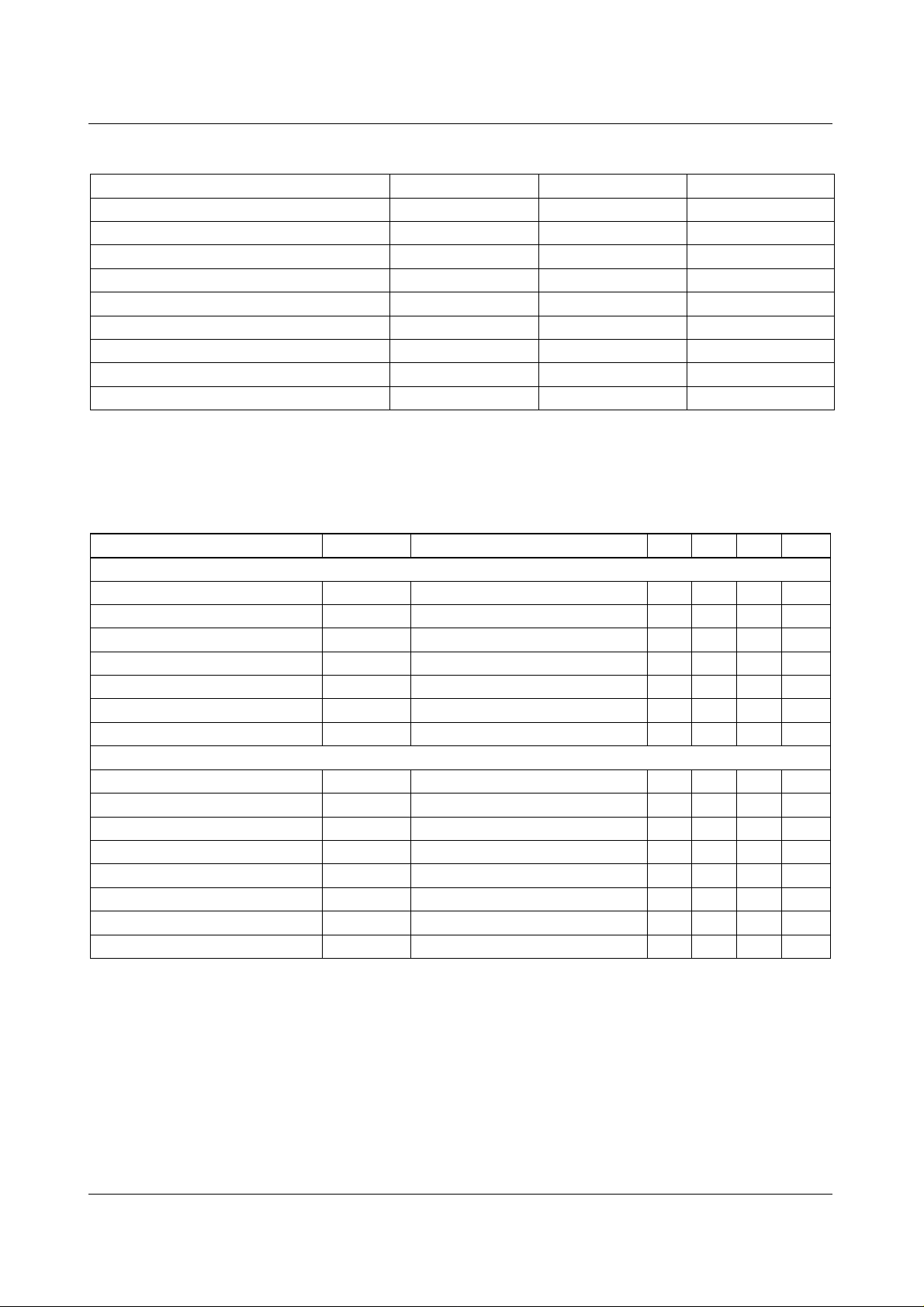
Internal Block Diagram
Description
UC3525A is a m onolithic integrated ci rcuit that Included
all of the control circuit necessary for a pulse width modulating regulator. There are a voltage reference, an error amplifier, a pulse width modulator, an oscillator, under-voltage
lockout, soft start circuit, and output drivers in the chip.
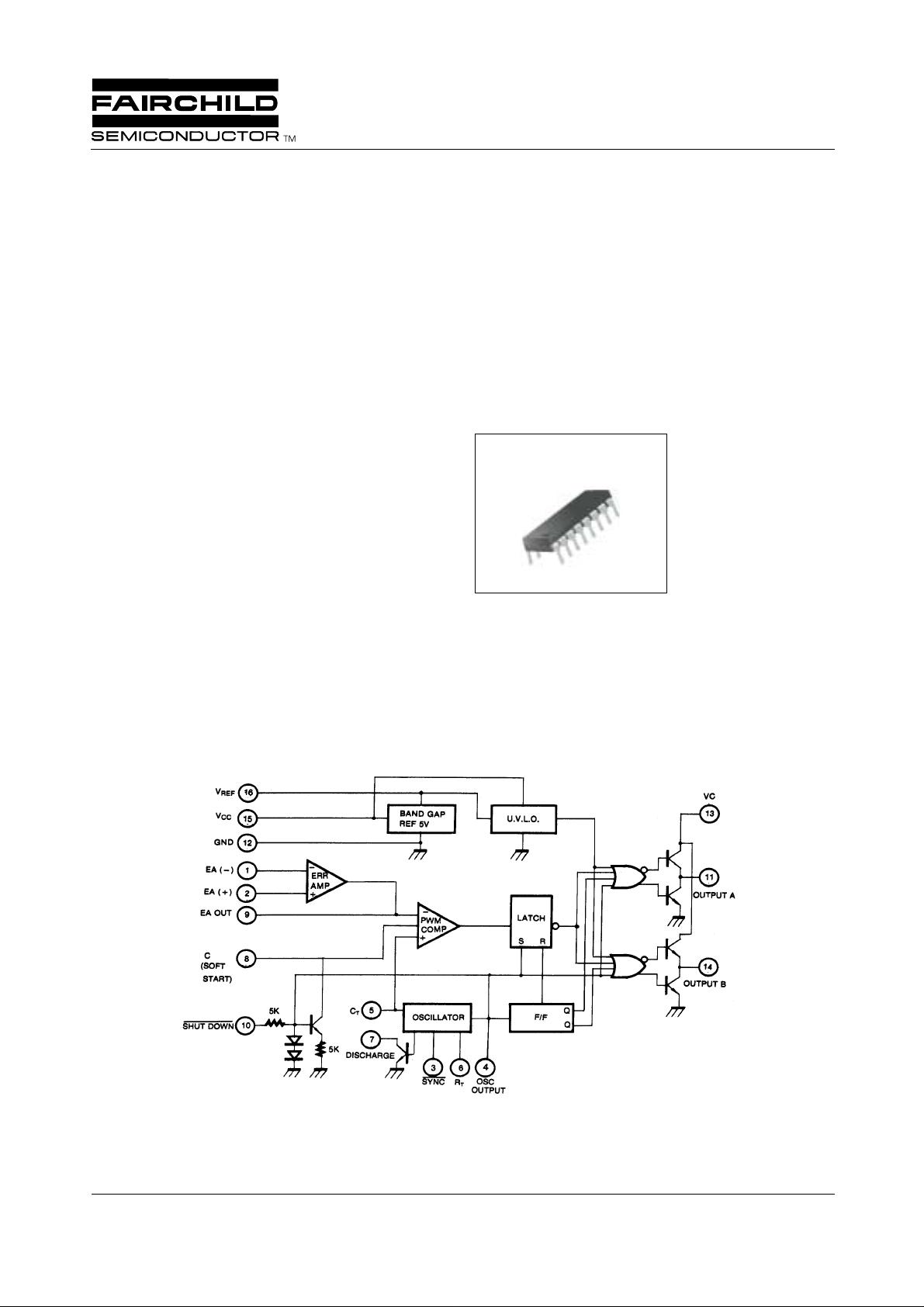
16-DIP
1
©2000 Fairchild Semiconductor International
Rev. 5.0
Page 2
UC3525A
Absolute Maximum Ratings
Parameter Symbol Value Unit
Supply Voltage V
Collector Supply Voltage V
Output Current, Sink or Source I
Reference Output Current I
Oscillator Charging Current I
Power Dissipation (T
= 25°C) P
A
REF
CHG(OSC)
Operating Temperature T
Storage Temperature T
Lead Temperature (Soldering, 10 sec) T
LEAD
Electrical Characteristics
(VCC = 20V, TA = -30°C to + 85°C, unless otherwise specified)
Parameter Symbol Conditions Min. Typ. Max. Unit
REFERENCE SECTION
Reference Output Voltage V
Line Regulation ∆V
Load Regulation ∆V
Short Circuit Output Current I
Total Output Variation (Note 1) ∆V
Temperature Stability (Note 1) ST
REF
REF
REF
SC
REF
T
Long Term Stability (Note 1) ST T
OSCILLATOR SECTION
Initial Accuracy (Note 1, 2) ACCUR T
Frequency Change With Voltage ∆f/∆V
Maximum Frequency f
Minimum Frequency f
Clock Amplitude (Note 1, 2) V
Clock Width (Note 1, 2) t
Sync Threshold V
Sync Input Current I
(MAX)
(MIN)
(CLK)
W(CLK)
TH(SYNC)
I(SYNC)
TJ = 25°C 5.0 5.1 5.2 V
VCC = 8 to 35V - 9 20 mV
I
= 0 to 20mA - 20 50 mV
REF
V
REF
Line, Load and Temperature 4.95 - 5.25 V
= 125°C ,1 KHR
J
= 25°C-± 3 ± 6%
J
V
CC
= 8 to 35V (Note 1, 2) - ± 0.8 ± 2%
CC
RT = 2KΩ, CT = 470pF 400 430 - KHz
RT = 200KΩ, CT = 0.1uF - 60 120 Hz
TJ = 25°C0.30.61µs
Sync = 3.5V - 1.3 2.5 mA
CC
C
O
40 V
40 V
500 mA
50 mA
5mA
D
OPR
STG
1000 m/W
0 ~ +70 °C
-65 ~ +150 °C
+300 °C
= 0, TJ = 25°C - 80 100 mA
- -2050mV
S
-2050mV
- 34- V
- 1.222.8V
2
Page 3
Electrical Characteristics
(VCC = 20V, TA = 0 to +85°C, unless otherwise specified)
Parameter Symbol Conditions Min. Typ. Max. Unit
ERROR AMPLIFIER SECTION (V
Input Offset Voltage V
Input Bias Current I
Input Offset Current I
Open Loop Voltage Gain G
Common Mode Rejection Ratio CMRR V
Power Supply Rejection Ratio PSRR V
PWM COMPARATOR SECTION
Minimum Duty Cycle D
Maximum Duty Cycle D
Input Threshold Voltage (Note 2) V
Input Threshold Voltage (Note 2) V
SOFT-START SECTION
Soft Start Current I
Soft Start Low Level Voltage V
Shutdown Threshold Voltage V
Shutdown Input Current I
OUTPUT SECTION
Low Output Voltage I V
Low Output Voltage II V
High Output Voltage I V
High Output Voltage II V
Under Voltage Lockout V
Collector Leakage Current I
Rise Time (Note 1) t
Fall Time (Note 1) t
STANDBY CURRENT
Supply Current I
CM
= 5.1V)
IO
BIAS
IO
VO
(MIN)
(MAX)
TH1
TH2
SOFT
SL
TH(SD)
N(SD)
OL I
OL II
CH I
CH II
UV
LKG
R
F
CC
UC3525A
- -1.510mV
- -110µA
- -0.11µA
≥10MΩ 60 80 - dB
R
L
= 1.5 to 5.2V 60 90 - dB
CM
= 8 to 3.5V 50 60 - dB
CC
- --0%
- 45 49 - %
Zero Duty Cycle 0.7 0.9 - V
Max Duty Cycle - 3.2 3.6 V
VSD = 0V, VSS = 0V 25 51 80 µA
VSD = 25V - 0.3 0.7 V
- 0.6 0.8 1 V
VSD = 2.5V - 0.3 1 mA
I
= 20mA - 0.1 0.4 V
SINK
I
= 100mA - 0.05 2 V
SINK
I
SOURCE
I
SOURCE
= 20mA 18 19 - V
= 100mA 17 18 - V
V8 and V9 = High 678V
VCC = 35V - 80 200 µA
CL = 1uF, TJ = 25°C - 80 600 ns
CL = 1uF, TJ = 25°C - 70 300 ns
VCC = 35V - 12 20 mA
Notes :
1. These parameters. although guaranteed over the recommended operating conditions, are not 100% tested in production
2. Tested at f
=40 KHz (RT =3.6K, CT =0.01uF, R
OSC
= 0Ω)
I
3
Page 4

UC3525A
Test Circuit
4
Page 5

Mechanical Dimensions
Package
6.40
±0.20
0.252
±0.008
16-DIP
0.81
0.032
()
UC3525A
#1
#8
7.62
0.300
#16
#9
MAX
19.80
0.780
0.128
3.25
±0.20
±0.008
19.40
0.764
±0.20
±0.008
0.38
0.014
±0.10
0.46
2.54
MIN
±0.004
0.018
0.100
±0.10
1.50
±0.004
0.059
0~15°
0.25
0.010
5.08
0.200
+0.10
–0.05
+0.004
–0.002
MAX
3.30
0.130
±0.30
±0.012
5
Page 6

UC3525A
Ordering Information
Product Number Package Operating Temperature
UC3525AN 16-DIP -30 ~ +85°C
6
Page 7

UC3525A
7
Page 8

UC3525A
LIFE SUPPORT POL I CY
FAIRCHILD’S PR ODUCTS ARE NOT AUTH ORIZED FOR USE AS C RITICAL COMPONENT S IN LIFE SUPPORT DE VICES
OR SYSTEMS WITHOUT THE EXPRESS WRITTEN APPROVAL OF THE PRESIDENT OF FAIRCHILD SEMICONDUCTOR
INTERNATIONAL. As used herein:
1. Life support devices or systems are devices or systems
which, (a) are intended for surgical implant into the body,
or (b) support or sustain life, and (c) whose failure to
perform when properly used in accordance with
2. A critical component in any component of a life support
device or sy stem whose fai lure to perform can be
reasonably expec ted to cause the failur e of the life support
device or system, or to affect its safety or effec t iv ene ss .
instructions for use provided in the labeling, can be
reasonably expected to result in a significant injury of the
user.
www.fairchildsemi.com
7/12/00 0.0m 001
2000 Fairchild Semiconductor International
Stock#DSxxxxxxxx
 Loading...