

Page 1
UC3175B
查询UC3175BDW供应商
Full-Bridge Power Amplifier
FEATURES DESCRIPTION
• Precision Current Control
±
800mA Load Current
•
• 1.25V Total V
• Controlled Velocity Head Parking
• Precision Dual Supply Monitor
with Indicator
• Limit Input to Force Output
Extremes
• Inhibit Input and UVLO
• 4V to 15V operation
SAT at 800mA
This full-bridge power amplifier is rated for continuous output current of 0.8 Amperes and is intended for use in demanding servo applications such as head
positioning for high-d ensi ty disk drives. The device includes a precision current
sense amplifier that provides accurate control of load current. Current is
sensed with a single resi s tor in seri es with the load. The power amplifier has a
very low output saturation voltage and will operate down to 4V supply levels.
Power output stage protection includes current l imiting and thermal shutdown.
Auxiliary functions on this device include a dual-input under-voltage comparator, which can monitor two independent supply voltages and force a built-in
head park function when either is below minimum. When activated by either the
UV comparator, or a command at the separate PARK input, the park circuitry
will override the amplifier i nputs to convert the power outputs to a programmable constant voltage source which will h old regula tion as th e supply voltage
falls to below 3.0 Volts. Added features include a POWER OK flag output, a
LIMIT input to force the drive output to its maximum level in either polarity, and
a over-riding INHIBIT input to disable al l amplifiers and reduce quiescent supply current.
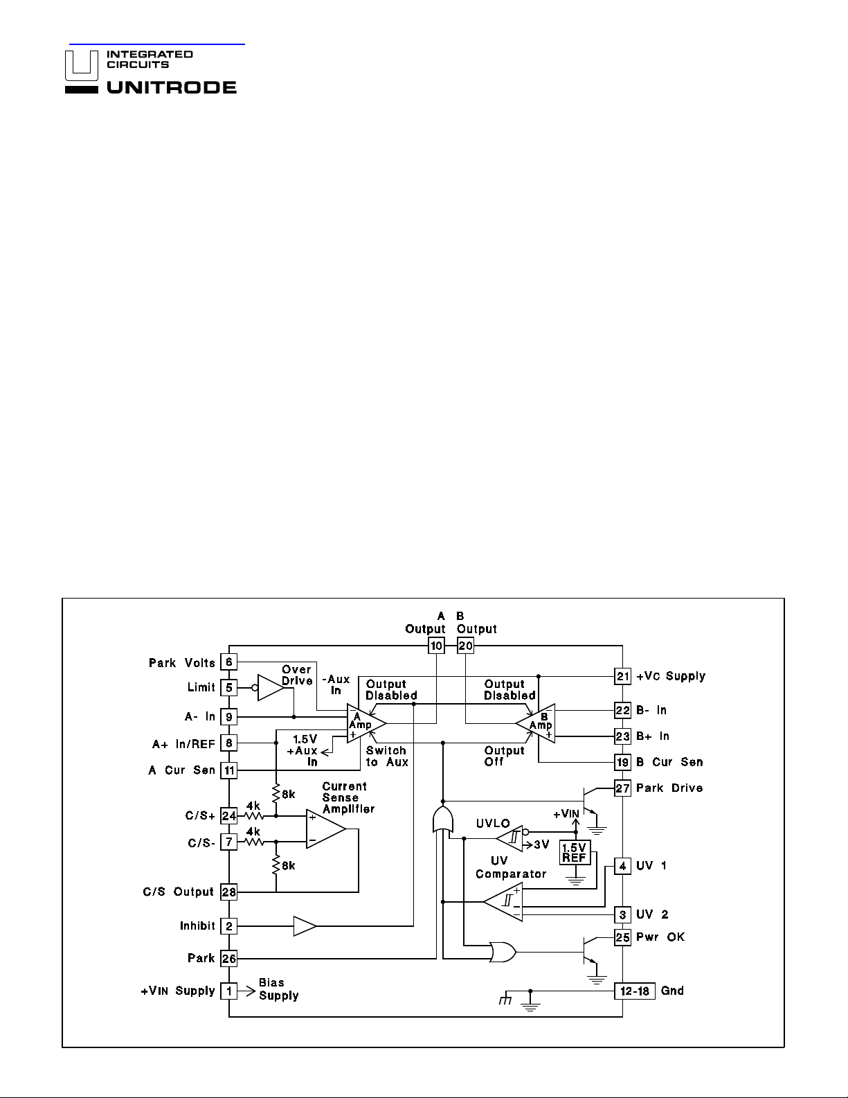
BLOCK DIAGRAM
This device is packaged in a power PLCC surface mount configuration which
maintains a standard 28-pin outline, but with 7 pins along one edge allocated to
ground for optimum thermal transfer. And is also available in a 24-pin surface
mount SOIC package.
Note: Pin numbers refer to PLCC packag e.
10/94
UDG-92054-1
Page 2
ABSOLUTE MAXIMUM RATINGS
Note 1: Unless other w ise indicat ed, volt age s are
reference d to grou nd and current s are pos itive
into, negat ive out of, the sp ecif ied te rminals.
"Pulsed" is defined as a less than 10% duty cycle
pulse with a maximum dur ation of 500µs.
Note 2: See Unitrode Int egr at ed Circ uits databoo k
for informat ion re gar ding ther ma l specif icat io ns
and limitat io ns of pack ages .
Unless otherwise stated spec ifications apply for 0°C ≤ TA ≤ 70°C, +VIN = 12V, +VC
= +VIN, A+/REF Inp ut = 6V. TA=TJ.
Input Supply Vo ltage, (+VIN,+VC). . . . . . . . . . . . . . . . . . . . . . . . . . . . . . . . 20V
UV Comparator, and Digital In put s
Maximum forced vo ltag e. . . . . . . . . . . . . . . . . . . . . . . . . . . . . -0.3V to 10V
Maximum forced cu rrent. . . . . . . . . . . . . . . . . . . . . . . . . . . . . . . . . ±10mA
C/S Inputs
Maximum forced vo ltag e. . . . . . . . . . . . . . . . . . . . . . . . . . . . . -0.3V to 20V
A and B Amplifier Inputs . . . . . . . . . . . . . . . . . . . . . . . . . . . . -0.3V to +V
Open Collector Out put Voltages. . . . . . . . . . . . . . . . . . . . . . . . . . . . . . . . . 20V
A and B Output Curren ts (continu ous)
Source . . . . . . . . . . . . . . . . . . . . . . . . . . . . . . . . . . . . . . . Internally Limited
Sink . . . . . . . . . . . . . . . . . . . . . . . . . . . . . . . . . . . . . . . . . . . . . . . . . . . 1.0A
Parking Drive Outp ut Curr ent
Continuous . . . . . . . . . . . . . . . . . . . . . . . . . . . . . . . . . . . . . . . . . . . 150mA
Pulsed . . . . . . . . . . . . . . . . . . . . . . . . . . . . . . . . . . . . . . . . . . . . . . . . . . . 1A
Output Diode Current (pulsed). . . . . . . . . . . . . . . . . . . . . . . . . . . . . . . . . . . 1A
Power OK Output Cu rrent (c ont inuous) . . . . . . . . . . . . . . . . . . . . . . . . . 30mA
Operating Jun ctio n Tem per atur e. . . . . . . . . . . . . . . . . . . . . . -55°C to +150 °C
Storage Temperature . . . . . . . . . . . . . . . . . . . . . . . . . . . . . . . -65 °C to +150 ° C
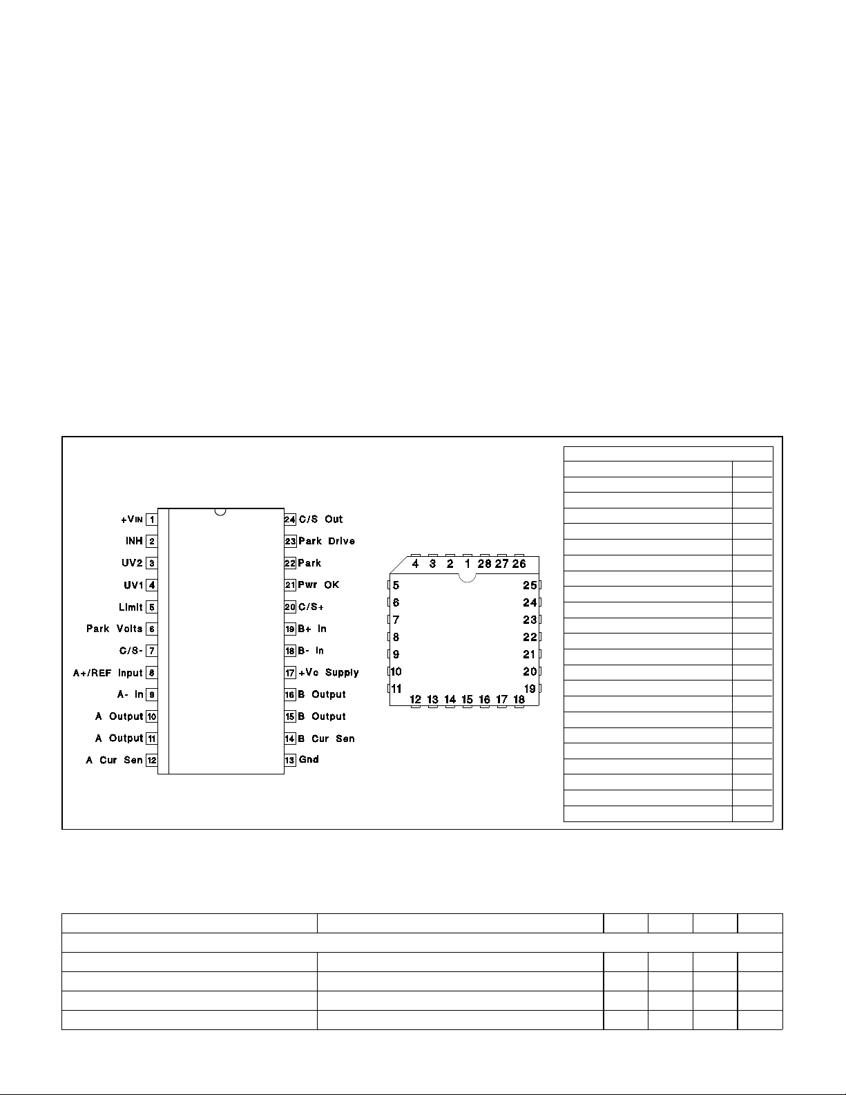
CONNECTION DIAG RAMS
IN
Thermal Data
QP Package:
Thermal Resistance Junction to Leads,
θ
JL . . . . . . . . . . . . . . . . . . . . . . . 15°C/ W
Thermal Resistance Junction to Ambient,
θ
JA . . . . . . . . . . . . . . . . . . . . . . . 4 0°C/W
UC3175B
SOIC-24 (Top View)
DW Package
PLCC-28 (Top View)
QP Package
PACKAGE PIN FUNCTION
FUNCTION PIN
+VIN 1
INH 2
UV2 3
UV1 4
Limit 5
Park Volts 6
C/S- 7
A+/REF Input 8
A- In 9
A Output 10
A Cur Sen 11
Gnd (Heat Dissipat io n Pins) 12-18
B Cur Sen 19
B Output 20
C Supply 21
+V
B- In 22
B+ In 23
C/S+ 24
Pwr OK 25
Park 26
Park Drive 27
C/S Out 28
ELECTRICAL CHARACTERISTICS:
PARAMETER TEST CONDITION S MIN TYP MAX UNITS
INPUT SUPPLY
+V
IN Supply Current All Amplifier Outpu ts = 6V 35 42 mA
+V
C Supply Current IOUT = 0A 1 mA
+V
IN UVLO Threshold Low to High 2.8 3. 0 V
UVLO Threshold Hysteresis 200 mV
2
Page 3

UC3175B
ELECTRICAL
CHARACTERISTICS (cont.)
Unless other wise stat ed sp ecif ic atio ns app ly for 0°C ≤ TA ≤ 70°C, +VIN = 12V, + V C = +VIN,
A+/REF INPUT = 6V. T
A=TJ.
PARAMETER TEST CONDITION S MIN TYP MAX UNITS
UNDER VOLTAGE (UV) COM PARATO R
Input Bias Current -1.5 -0.5 µA
UV Thresholds Low to High, Other Input = 5V 1.48 1.50 1.52 V
UV Threshold Hyst eresis 15 25 40 mV
Pwr OK V
Pwr OK Leakage V
SAT IOUT = 5mA 0.45 V
OUT = 20V 5 µA
POWER AMPLI FI ERS A and B
Input Offset Voltage V
CM = 6V, A Amplifie r 8 mV
B Amplifier 12 mV
Input Off set Drift No te 1, A Amp lifier On ly 25 µV/°C
Input Bias Current V
Input Offset Current V
Input Bias Cu rrent at A+/Ref Input (A+/Ref–C/S+)/12k, T
CMRR 1V ≤ V
PSRR +V
Large Signal Volta ge G ai n V
CM = 6V, except A+ /REF Input -500 -150 nA
CM = 6V, B Amplifie r Only 200 nA
J = 25°C 60 84 105 µA/V
CM ≤ 10V 70 90 dB
IN = 4V to 15V, VCM = 1.5V 70 90 dB
OUT = 1V, Sinking 500mA to VOUT = 11V,
Sourcin g 500m A 3.0 15.0 V/mV
Slew Rate 1 to 13V, 13 to 1V, T
J = 25°C12.1V/µs
Unity Gain Bandwidt h Note 1, A Amplifier 2 MHz
Note 1, B Am p l ifi er 1 MHz
High-Side Current Limit 0.8 1.0 A
Output Saturation Voltage High-Side, I
High-Side, I
Low-Side, I
SOURCE = 250mA 0.7 V
SOURCE = 800mA 0.85 V
SINK = 250mA 0. 3 V
Low-Side, ISINK = 800m A 0.4 V
Total, I
OUT = 250mA 1.0 1.2 V
Total, I
OUT = 800mA 1.25 1.6 V
High Side Diode V
Low Side Diode V
F ID = 800mA, Inhibit Ac tivated 1.0 V
F ID = 800mA, Inhibit Ac tiva ted 1.0 V
CURRENT SENSE AMPLIFIER
Input Offset Voltage V
Input Offset Change with Common Mode 0V ≤ V
CM = 6V 2.0 mV
CM ≤ 12V
Input 1500 µV/V
Input Offset Drift Note 1 8 µV/°C
Voltage Gain -1.0V ≤ V
Output Satu ration Volt age Low-Side, I
High-Side, I
Maximum A+/ Ref Input Vo lts Below + V
10mA Output Current, +V
DIFF ≤ +1. 0V, VCM = 6V 1.95 2.00 2.05 V
SINK = 1.5mA 0.3 0.5 V
SOURCE = 1.5mA 0.4 0.7 V
IN, C/S+ & C/S- = BOUTPUT Max @
IN = 4.5V, C/S VIO ≤ 5mV 2.6 3.0 V
PARKING FUNCTION
Park Input Threshold 0.7 1.1 1.7 V
Park Input Current Park Input = 1.7V 60 100 µA
Park Drive Satura tion Voltag e, PD
Parking Drive Leakage V
VSAT ISINK = 100mA 0.3 0.5 V
OUT = 20V 100 µA
Amplifier A Aux Input Bias Current -500 - 150 nA
3
Page 4

UC3175B
ELECTRICAL
CHARACTERISTICS (cont.)
PARAMETER TEST CONDITION S MIN TYP MAX UNITS
PARKING FUNCTIONS (cont .)
Amplifier A Satura tion Voltag e, A
Regulating Volt age at Park Volts 1.47 1.50 1.53 V
Minimum Parking Supply Voltage A
AUXILIARY FUNCTIONS
Limit Input Low Voltage A Output Forced Low 0.7 0.8 V
Limit Input High Voltage A O utpu t Forced H igh 2.2 2.3 V
Limi t Inactive 1.2 1.8 V
Limit Open Circuit Voltage 1.45 1.50 1.55 V
Limit Input Resistance 1.2V ≤ Limit Input ≤ 1.8V 10 kΩ
Inhibit Input Threshol d 0.7 1.1 1.7 V
Inhibit Input Current I n hibit Input = 1. 7 V 400 700 µA
Supply Curren t whe n Inhibite d The sum of +V
Thermal Shutdown Tempe ratur e 165 °C
Unless other wise stat ed sp ecif ic atio ns app ly for 0°C ≤ TA ≤ 70°C, +VIN = 12V, + V C = +VIN,
A+/REF Input = 6V. T
HVSAT ISOURCE = 50mA, +V IN = 3V 0.65 0.8 V
HVSAT + PDVSAT ≤ 1.3V @ 50mA 1.7 1.9 V
A=TJ.
IN and +VC current s 2 6 mA
Note 1: This specifica tion not teste d in prod uct ion.
UC3175B Series Current Sensing
UDG-92058
G
I
L
O
=
=
V
S
Rfa
Rfb
• 2 •
R
S
4
Page 5

Parking Function
UC3175B
Notes: Parking voltage
RP is optional for current limiting.
Inhibit and Park Input s are active high.
Pwr OK is low on power failure.
=
1.5V
R2 −
UDG-92059
• R1 + R2
(IL • RP)
UNITRODE INTEGRATED CIRCUITS
7 CONTINENTAL BLVD. • MERRIMACK, NH 03054
TEL. (603) 424-2410 • FAX (603) 424-3460
5
Page 6

IMPORTANT NOTICE
T exas Instruments and its subsidiaries (TI) reserve the right to make changes to their products or to discontinue
any product or service without notice, and advise customers to obtain the latest version of relevant information
to verify, before placing orders, that information being relied on is current and complete. All products are sold
subject to the terms and conditions of sale supplied at the time of order acknowledgement, including those
pertaining to warranty, patent infringement, and limitation of liability.
TI warrants performance of its semiconductor products to the specifications applicable at the time of sale in
accordance with TI’s standard warranty. Testing and other quality control techniques are utilized to the extent
TI deems necessary to support this warranty . Specific testing of all parameters of each device is not necessarily
performed, except those mandated by government requirements.
CERTAIN APPLICA TIONS USING SEMICONDUCT OR PRODUCTS MAY INVOLVE POTENTIAL RISKS OF
DEATH, PERSONAL INJURY, OR SEVERE PROPERTY OR ENVIRONMENTAL DAMAGE (“CRITICAL
APPLICATIONS”). TI SEMICONDUCTOR PRODUCTS ARE NOT DESIGNED, AUTHORIZED, OR
WARRANTED TO BE SUITABLE FOR USE IN LIFE-SUPPORT DEVICES OR SYSTEMS OR OTHER
CRITICAL APPLICA TIONS. INCLUSION OF TI PRODUCTS IN SUCH APPLICATIONS IS UNDERST OOD TO
BE FULLY AT THE CUSTOMER’S RISK.
In order to minimize risks associated with the customer’s applications, adequate design and operating
safeguards must be provided by the customer to minimize inherent or procedural hazards.
TI assumes no liability for applications assistance or customer product design. TI does not warrant or represent
that any license, either express or implied, is granted under any patent right, copyright, mask work right, or other
intellectual property right of TI covering or relating to any combination, machine, or process in which such
semiconductor products or services might be or are used. TI’s publication of information regarding any third
party’s products or services does not constitute TI’s approval, warranty or endorsement thereof.
Copyright 1999, Texas Instruments Incorporated
 Loading...