

Page 1
查询UC3173ADW供应商
Full Bridge Power Amplifier
UC3173A
FEATURES
• Precision Current Control
•±500mA Load Current
• 1.3V Typical Total V
• Controlled Velocity Head Parking
• Precision Dual Supply Monitor with
Indicator
• Range Control for 4:1 Gain Change
• Compensation Adjust Pin for
Bandwidth Control
• Inhibit Input and UVLO
• 5V or 12V Operation
• 12mA Quiescent Supply Current
• PLCC, SOIC, and Low Profile Quad
Flat Pack Packages
SAT
at 550mA
DESCRIPTION
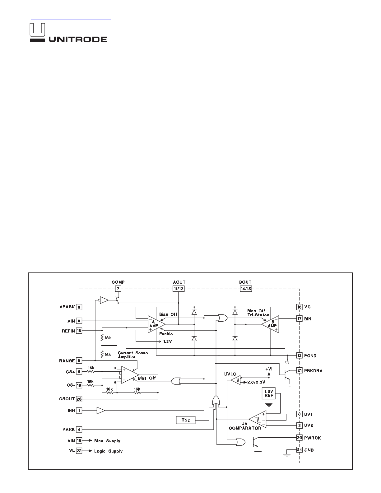
This full bridge power amplifier, rated for continuous output current of
0.55A, is intended for use in demanding servo applications such as head
positioning for high density disk drives. This device includes a precision current sense amplifier that senses load current with a single resistor in series
with the load. The UC3173A is optimized to consume a minimum of supply
current, and is designed to operate in both 5V and 12V systems. The power
output stages have a low saturation voltage and are protected with current
limiting and thermal shutdown. When inhibited the device will draw less
than 1.5mA of total supply current.
Auxiliary functions on this device include a dual input undervoltage comparator, which can monitor two independent supply voltages and activate
the built in head park function when either is below minimum. The park circuitry allows a programmable retract voltage to be applied to the load for
limiting maximum head velocity. A separate low side parking drive pin permits a series impedance to be inserted to control maximum retract current.
The parking drive function can be configured to operate with supply voltages as low as 1.2V.
The closed loop transconductance of the configured power amplifier can be
switched between a high and low range with a logic input. The 4:1 change
in gain can be used to extend the dynamic range of the servo loop. Bandwidth variations that would otherwise result with the gain change can be
controlled with a compensation adjust pin.
BLOCK DIAGRAM
04/99
UDG-94039
Page 2
UC3173A
ABSOLUTE MAXIMUM RATINGS (Note 1)
Input Supply Voltage, (VIN, VC, VL) . . . . . . . . . . . . . . . . . . 20V
UV Comparator
Maximum Forced Voltage . . . . . . . . . . . . . . . . −0.3V to 10V
Maximum Forced Current. . . . . . . . . . . . . . . . . . . . .±10mA
B Amplifier Inverting Input . . . . . . . . . . . . . . −0.3V to VIN + 1.0
A Amplifier Inverting Inputs,
(Aux. and Normal) . . . . . . . . . . . . . . . . . −0.3V to VC + 1.0V
Open Collector Output Voltages . . . . . . . . . . . . . . . . . . . . . 20V
A and B Output Currents (Continuous)
Source . . . . . . . . . . . . . . . . . . . . . . . . . . . . Internally Limited
Sink . . . . . . . . . . . . . . . . . . . . . . . . . . . . . . . . . . . . . . . . 0.6A
Parking Drive Output Current
Continuous . . . . . . . . . . . . . . . . . . . . . . . . . . . . . . . . 150mA
Pulsed. . . . . . . . . . . . . . . . . . . . . . . . . . . . . . . . . . . . . . . . 1A
Output Diode Current (Pulsed). . . . . . . . . . . . . . . . . . . . . . 0.6A
Power OK Output Current (Continuous). . . . . . . . . . . . . . 30mA
Operating Junction Temperature . . . . . . . . . . −55°C to +150°C
Storage Temperature . . . . . . . . . . . . . . . . . . . −65°C to +150°C
Lead Temperature . . . . . . . . . . . . . . . . . . . . . . . . . . . . . +300°C
Note 1: Unless otherwise indicated, voltages are referenced to
ground and currents are positive into, negative out of, the specified terminals, “Pulsed” is defined as a less than 10% duty cycle
pulse with a maximum duration of 500
µ
s.
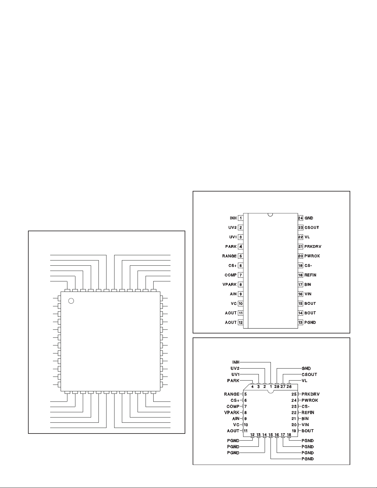
CONNECTION DIAGRAMS
THERMAL DATA
DW Package:
Thermal Resistance Junction to Leads, θjl . . . . . . . . 35°C/W
Thermal Resistance Junction to Ambient, θja . . . . 60-70°C/W
FQ Package:
Thermal Resistance Junction to Leads, θjl. . . . . . . . . 60°C/W
Thermal Resistance Junction to Ambient, θja . . 110-120°C/W
QP Package:
Thermal Resistance Junction to Leads, θjl. . . . . . . . . 15°C/W
Thermal Resistance Junction to Ambient, θja . . . . 30-40°C/W
Note 2: The above numbers forθjl are maximums for the limiting
thermal resistance of the package in a standard mounting configuration. Theθja numbers are meant to be guide lines for the
thermal performance of the device/pc-board system. All of the
above numbers assume no ambient airflow.
Note 3: Consult Packaging Section of Unitrode Integrated Circuits databook for thermal specifications and limitations of packages.
SOIC-24 (Top View)
DW Package
TQFP-48 (Top View)
FQ Package
N/C
N/C
REFIN
CS–
PWROK
PRKDRV
48
46
N/C
VL
CSOUT
GND
N/C
N/C
N/C
N/C
INH
UV2
UV1
PARK
RANGE
CS+
COMP
VP ARK
N/C
47
1
2
3
4
5
6
7
8
9
10
11
12
13
15
14
N/C
N/C
BIN
VIN
N/C
N/C
42
44
43
45
17
18
16
40
393837
41
19
20
23
21
22
N/C
36
35
BOUT
BOUT
34
N/C
33
N/C
32
PGND
31
PGND
30
N/C
29
N/C
28
AOUT
27
26
AOUT
25
N/C
24
N/C
N/C
VC
AIN
N/C
N/CN/C
PLCC-28 (Top View)
QP Package
2
Page 3
UC3173A
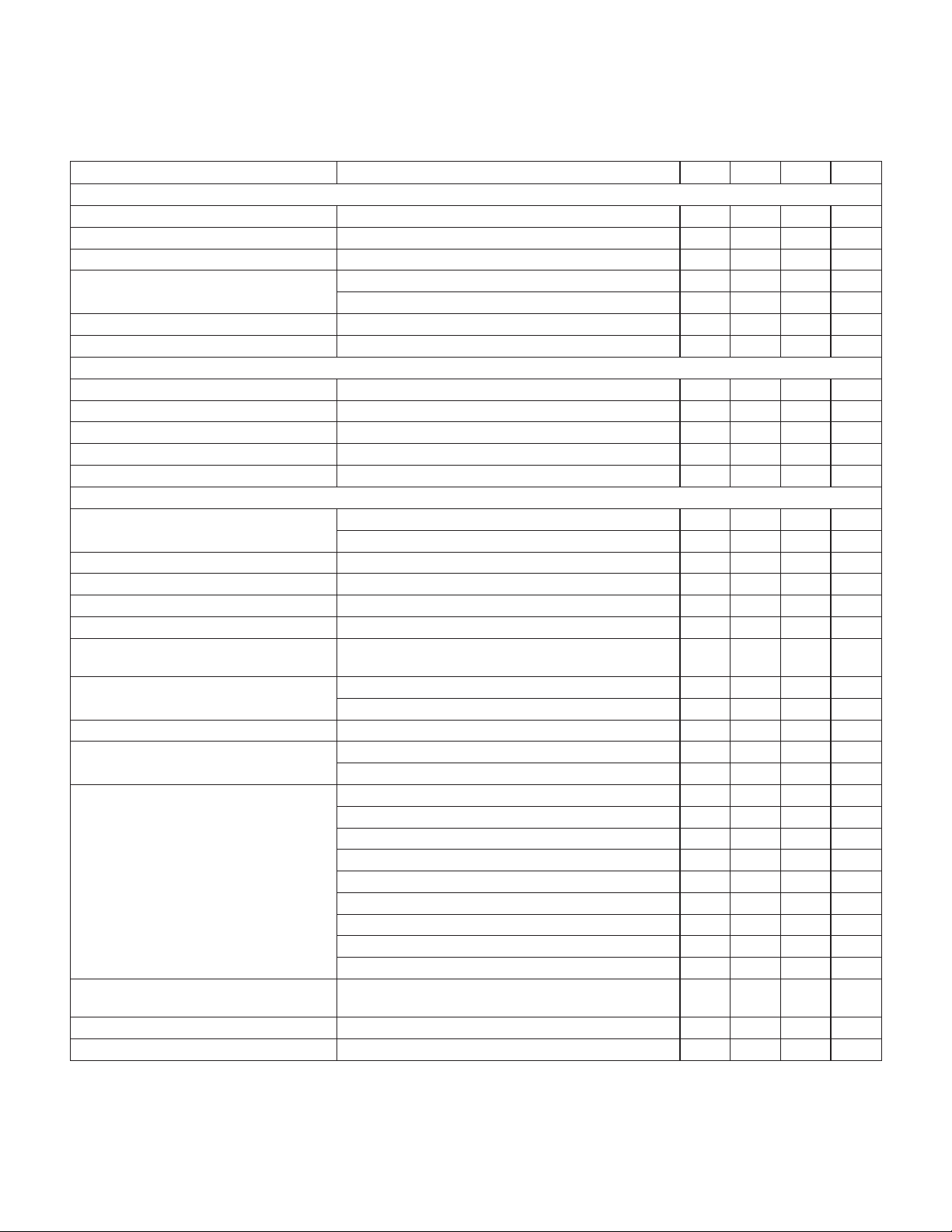
ELECTRICAL CHARACTERISTICS:
Unless otherwise stated, these specifications apply for TA= 0 to +70°C, VIN = 5V,
VC = VIN = VL, REFIN = VIN/2, RANGE, PARK, and INH = 0V, and TA=TJ.
PARAMETER TEST CONDITIONS MIN TYP MAX UNITS
Input Supply
VIN Supply Current 10 13 mA
VC Supply Current I
= 0A 1.2 2.0 mA
OUT
VL Supply Current 0.65 1.0 mA
Total Supply Current Supplies = 5V, I
Supplies = 12V, I
= 0A 12 16 mA
OUT
= 0A 13 18 mA
OUT
VL UVLO Threshold Low to High 2.6 2.8 V
UVLO Threshold Hysteresis 300 mV
Under Voltage (UV) Comparator
Input Bias Current Max at Either UV Input −0.25 −1.0 µA
UV Thresholds Low to High, Other Input = 5V 1.28 1.3 1.32 V
UV Threshold Hysteresis 19 24 29 mV
PWROK Vsat I
PWROK Leakage V
= 5mA, UV Input Low 0.15 0.45 V
OUT
= 20V 5 µA
OUT
Power Amplifiers A and B
Input Offset Voltage A Amplifier, VCM= 2.5V 4 mV
B Amplifier, V
Input Bias Current V
= 2.5V, Inverting Inputs Only −150 −500 nA
CM
Input Bias Current at Ref. Input (REFIN − CS+)/48kΩ,T
CMRR V
= 1V to 10V, Supplies = 12V 70 90 dB
CM
PSRR VIN = 4V to 15V, V
Large Signal Voltage Gain Supplies = 12V, V
V
= 11V, I
OUT
= 2.5V 12 mV
CM
= 25°C 152127µA/V
J
= 1.5V 70 90 dB
CM
OUT
= 1V, I
OUT
= −300mA
= 300mA to
OUT
3.0 15.0 V/mV
Gain Bandwidth Product A Amplifier (Note 4) 2.0 MHz
B Amplifier (Note 4) 1.0 MHz
Slew Rate (Note 4) 1.0 V/µs
High-Side Current Limit Low Range Mode 0.6 0.8 A
High Range Mode 1.1 1.6 A
Output Saturation Voltage High-Side, I
High-Side, I
High-Side, I
Low-Side, I
Low-Side, I
Low-Side, I
Total V
SAT,IOUT
Total V
SAT,IOUT
Total V
SAT,IOUT
VC to VIN Headroom Volts below VIN, delta High-Side, V
= −100mA (Note 5) 0.7 V
OUT
= −300mA (Note 5) 0.8 V
OUT
= −550mA (Note 5) 0.95 V
OUT
= 100mA 0.2 V
OUT
= 300mA 0.25 V
OUT
= 550mA 0.35 V
OUT
= 100mA 0.9 1.2 V
= 300mA 1.05 1.4 V
= 550mA 1.3 1.7 V
= 100mV, I
SAT
0.23 0.4 V
OUT
= −550mA (Note 5)
High-Side Diode, V
Low-Side Diode, V
F
F
ID= 550mA 1.0 V
ID= 550mA, INH Activated, B Amplifer Only 1.0 V
3
Page 4
UC3173A
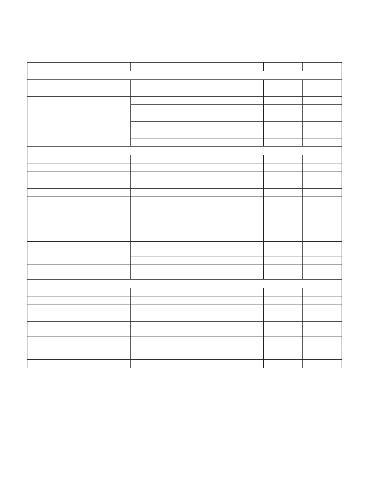
ELECTRICAL CHARACTERISTICS:
Unless otherwise stated, these specifications apply for TA= 0 to +70°C, VIN = 5V,
VC = VIN = VL, REFIN = VIN/2, RANGE, PARK, and INH = 0V, and TA=TJ.
PARAMETER TEST CONDITIONS MIN TYP MAX UNITS
Current Sense Amplifier
Input Offset Voltage V
Input Offset Change with Common
Mode Input
Voltage Gain V
Saturation Voltage Low-Side, I
= 2.5V, Low range mode 2.0 mV
CM
= 2.5V, High range mode 4.0 mV
V
CM
= –1V to 13V, Supplies = 12V, Low Range Mode 2000 µV/V
V
CM
= –1V to 13V, Supplies = 12V, High Range Mode 4000 µV/V
V
CM
= +1.0 to −1.0V, VCM= 2.5V, High Range Mode 0.485 0.50 0.515 V/V
DIFF
= +1.0 to −1.0V, VCM= 2.5V, Low Range Mode 1.95 2.0 2.05 V/V
V
DIFF
= 1mA 0.1 0.3 V
OUT
High-Side, I
= −1mA, Referenced to VIN 0.1 0.3 V
OUT
Parking Function
Park Input Threshold Voltage 0.6 1.1 1.7 V
Park Input Threshold Current Internal Pull-Up, VIN = 0.6V 50 75 µA
Park Drive Saturation Voltage I
Park Drive Leakage V
= 50mA 0.15 0.35 V
OUT
= 20V 50 µA
OUT
Regulating Voltage at Park Volts Input 1.275 1.30 1.325 V
Amplifier A Auxiliary Input Bias Current −300 −750 nA
Amplifier A Parking High-Side
Saturation Voltage
= −50mA, VIN = 0V, VC = VL = 5V, PARK Open,
I
OUT
VC to V
OUT
Minimum Parking Supply At VC and VL, VIN = 0V,
A Amplifier Out - V
SAT
PRKDRV > 0.5V, I
PARK
=
0.8 0.95 V
1.4 1.7 V
50mA
Minimum Supply for Parking Drive and
Power OK Operation
At VL, VC = VIN = 0V, V
I
PRKDRV = 50mA, Rl = 30Ω to 2V
OUT
PWROK = 5mA, Rl = 300Ω to 2V 1.2 1.6 V
I
OUT
SAT
< 0.5V,
VL Parking Supply Current PARK Open, VL = 5V, VC = 1.6V, VIN = 0V,
PWROK I
= 5mA, PRKDRV I
OUT
OUT
= 50mA
1.1 1.4 V
1.6 3.0 mA
Auxiliary Functions
Inhibit Input Threshold 0.6 1.1 1.7 V
Inhibit Input Current INH = 1.7V −0.5 −1.0 µA
Range Input Threshold 0.6 1.1 1.7 V
Range Input Current RANGE = 1.7V 50 100 µA
Comp Adjust Pin Saturation Voltage RANGE = 0V, Pin Current = ±500µA,
Referenced to A
OUT
Comp Adjust Leakage Current RANGE = 1.7V, Supplies = 12V,
A
OUT-VCOMP
= ±6V
0.02 0.1 V
5 µA
Total Supply Current when Inhibited VIN, VC, and VL currents 1.0 1.5 mA
Thermal Shutdown Temperature (Note 4) 165 °C
Note 4: Guaranteed by design. Not 100% tested in production.
Note 5: The high-side saturation performance of the UC3173A is referenced to the VIN supply pin.
The VC supply pin can operate about 400mV below the VIN supply input without affecting the performance.
4
Page 5

PIN DESCRIPTIONS
AIN: Inverting input to the A amplifier. Used as the sum-
ming node to close the loop on the overall power amplifier.
UC3173A
PARK: Input that forces the park condition on the
UC3173A. This input has an internal pull-up that will
force the park condition if the pin is left open.
AOUT: Output for the A power amplifier, providing one
end of the differential drive to the load during normal operation and during park. During a UVLO condition at the
VIN supply pin, this output is forced to a high, source
only state. When the UC3173A is inhibited, this output
will be set high, in a source only state.
BIN: Inverting input to the B amplifier. Used to program
the gain of the B amplifier to guarantee maximum voltage swing to the load.
BOUT: Output for the B power amplifier, providing one
end of the differential drive to the load during normal operation. During park and while inhibited this pin is
tristated.
COMP: The compensation adjust pin allows the user to
provide an auxiliary compensation network for the A amplifier that is only active when the current sense amplifier
is in the low range. With this option, the user can control
the change in bandwidth that would otherwise result
from the gain change in the feedback loop.
CS–: The inverting input to the current sense amplifier is
typically tied to the load side of the series current sense
resistor. This pin can be pulled below ground during an
abrupt load current change with an inductive load.
Proper operation of the current sense amplifier will result
if this pin does not go below ground by an amount
greater than: REFIN / 2 –0.3V, in low range mode, and 2
• REFIN –0.9V, in high range mode.
CS+: The noninverting input to the current sense ampli-
fier is typically tied to the connection between the A amplifier output and the current sense resistor connected in
series with the load.
CSOUT: The output of the current sense amplifier has a
1.5mA current source pull-up and an active NPN
pull-down. The output will pull to within 0.3V of either rail
with a load current of less than 1mA.
GND: Reference point for the internal reference, UV
comparator, and other low level circuitry.
INH: A high impedence logic input that disables the A
and B power amplifiers, as well as the Current Sense
amplifier. The UV comparators and logic functions of the
UC3173A remain active. This input has an internal
pull-up that will inhibit the device if the input is left open.
The Inhibit function is overridden by any condition that
forces the Park function to be activated.
PGND: Current return for all high level circuitry, this pin
should be connected to the same potential as GND.
PRKDRV: A 100mA drive output that is active low during
a park operation. This pin is normally used to supply the
lowside drive to the load during parking, in place of the B
amplifier. A series resistor can be added between this
pin and the load to limit current during park.
PWROK: Indicates with an active low condition that either of the UV inputs are low, or that the supply voltage
at the VL input to the UC3173A has dropped below the
UVLO threshold. This output will remain active low until
the VL supply has dropped to below approximately 1.2V.
RANGE: When this pin is open or at a logic low potential, the current sense amplifier will be in its low range
mode. In this mode the voltage gain of the amplifier will
be 2. If this pin is brought to a logic high, the gain of the
current sense amplifier will change into its high range
value of 0.5. This factor of four change in gain will vary
the overall transconductance of the power amplifier by
the same ratio, with the transconductance being the
highest in the high mode. This feature allows improved
dynamic range of load current control for a given control
input range and resolution.
REFIN: Reference for input control signals to the power
amplifier, as well as, the noninverting inputs to the A and
B amplifiers, and the output level shift for the CS amplifier.
VC: High current supply to the collectors of the high side
NPN output devices on the A and B amplifiers. This supply should be powered whenever the A or B amplifiers
are activated.This pin can operate approximately 400mV
below the VIN supply without affecting the voltage available to the load. This supply pin provides drive to the
power amplifiers during a parking operation.
VIN: Provides bias supply to both the power amplifiers
and the current sense amplifiers. The high-side drive to
the power stages on both the A and B amplifiers is referenced to this pin. The high side saturation voltages are
specified and measured with respect to this supply pin.
The parking function of the device is fully operational independent of the voltage at this pin.
5
Page 6
PIN DESCRIPTIONS (cont.)
VL: Logic portions of the UC3173A are powered by this
supply pin, including the reference, UVLO, the UV comparators, and the PRKDRV and PWROK outputs. This
pin is a low current supply that would normally be tied to
the VC pin, or to a parking hold up capacitor for extended parking operation with very low recovered back
emf.
UC3173A
by any one of the following four conditions, 1: a low condition on either of the UV inputs, 2: a high input level at
the Park input, 3: a UVLO condition at the VL supply pin,
and 4: activation of the TSD, (thermal shutdown) protection circuit. During a UVLO condition at the VL pin the
auxiliary inputs to the A amplifier are over-ridden, and
the A amplifier output is forced to its high state.
VPARK: The auxiliary inverting input to the A amplifier,
activated during park conditions on the UC3173A. An internal auxiliary non-inverting input is connected to the
1.3V reference. When the auxiliary inputs are activated,
the A amplifier will force a programmed voltage at its output for a maximum back-emf/velocity retract of the head.
The park condition on the UC3173A is always activated
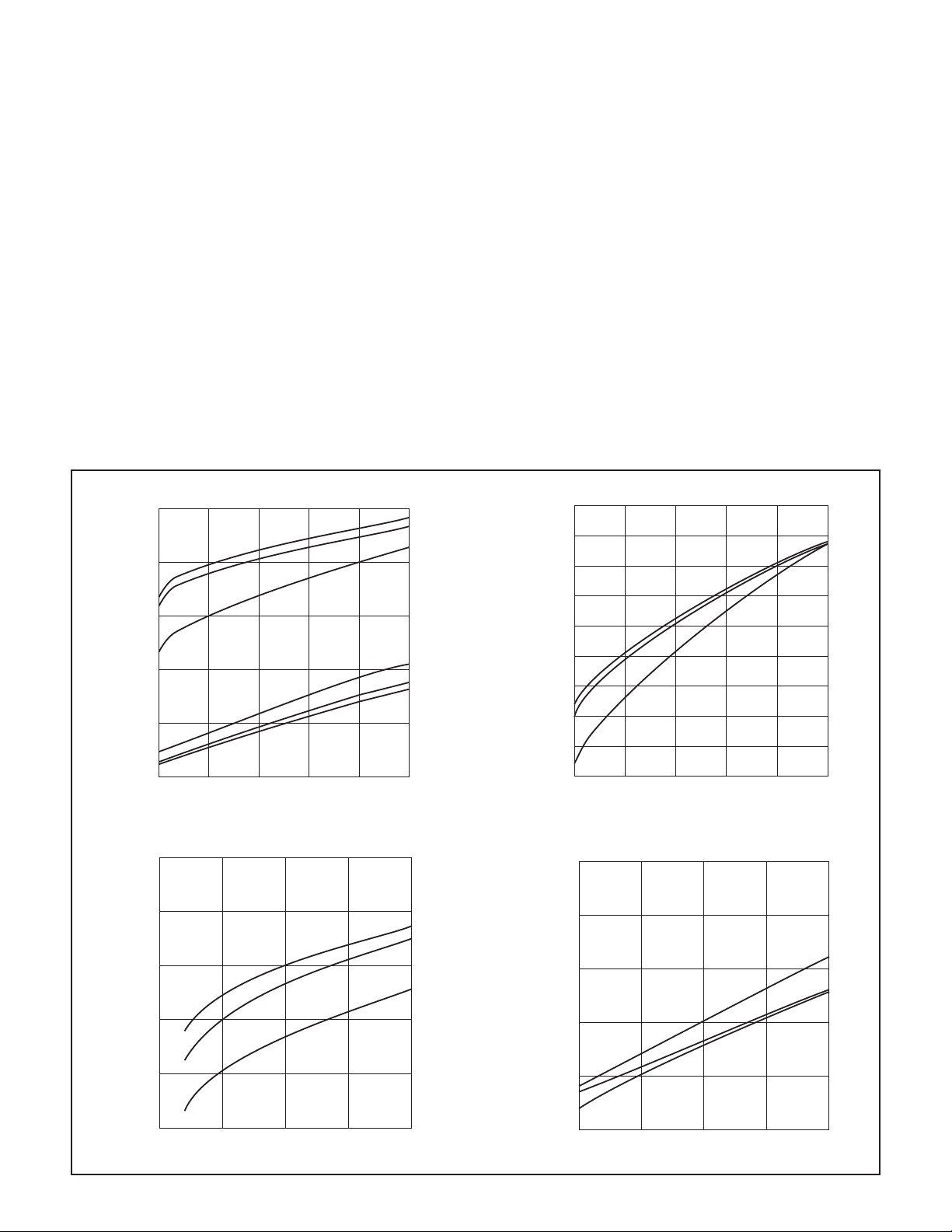
APPLICATION INFORMATION
A and B Amplifier High and LowV
1
0.8
0.6
SA T
0.4
V(Volts)
0.2
HIGH-SIDE
LOW-SIDE
0°C
125°C
125°C
0°C
SATS
25°C
25°C
UV1&2:Inputs to the UV comparator, these inputs are
high impedance sensing points used to monitor external
supply conditions. Either of the inputs going low will force
the device into a park condition, and force the PWROK
output to an active low state. If either of these inputs is
not used it should be connected to a voltage greater
than 1.3V.
A and B AmplifierTotal V
1.4
1.3
1.2
1.1
1.0
SA T
0.9
Total V (Volts)
0.8
0.7
0.6
25°C
0°C
SAT
125°C
0
0 100 200 300 400 500
Output Current (mA)
VINtoVCHeadroom
1
0.8
0.6
0.4
0°C
25°C
VIN - VC (Volts)
0.2
0
0 50 100 150 200
A or B Amplifier High-Side V Increase (mVolts)
125°C
SA T
I=
OUT
450mA
0.5
0 100 200 300 400 500
Output Current (mA)
PWROK Saturation Voltage
0.5
0.4
0.3
SA T
0.2
125°C
0°C
Power OK V (Volts)
0.1
0
0 5 10 15 20
25°C
Pow er OK Output Current (mA)
6
Page 7
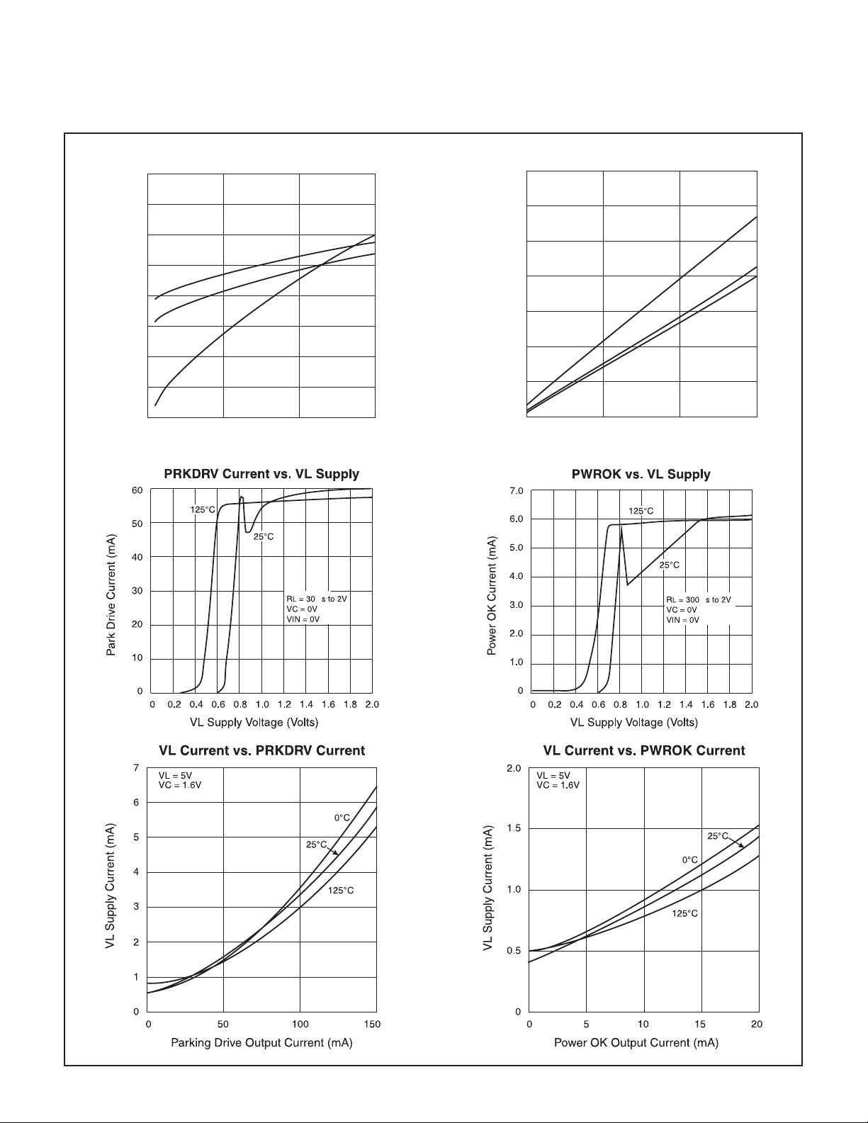
APPLICATION INFORMATION (cont.)
UC3173A
A Amplifier High-SideV in Park Mode
1.2
1.1
1.0
0.9
0.8
25°C
0.7
0.6
0.5
0°C
125°C
SAT
VIN = 0V
VC = VL = 2V
A Amp High-Side SAT (VC to AOUT) (Volts)
0.4
0 100 200 300
Output Current (mA)
PRKDRV Saturation Voltage
0.7
0.6
0.5
SA T
0.4
0.3
0.2
ParkingDriveV (Volts)
0.1
0
0 10 100 150
Output Current (mA)
125°C
25°C
0°C
Ω
Ω
7
Page 8
APPLICATION INFORMATION (cont.)
UC3173A
IL
GM =
=
V
SFBFA CS S
R
•
RIAV R
AV
=Current Sense Amplifier Gain = 2.0 Low Range, 0.5 High Range
•
CS
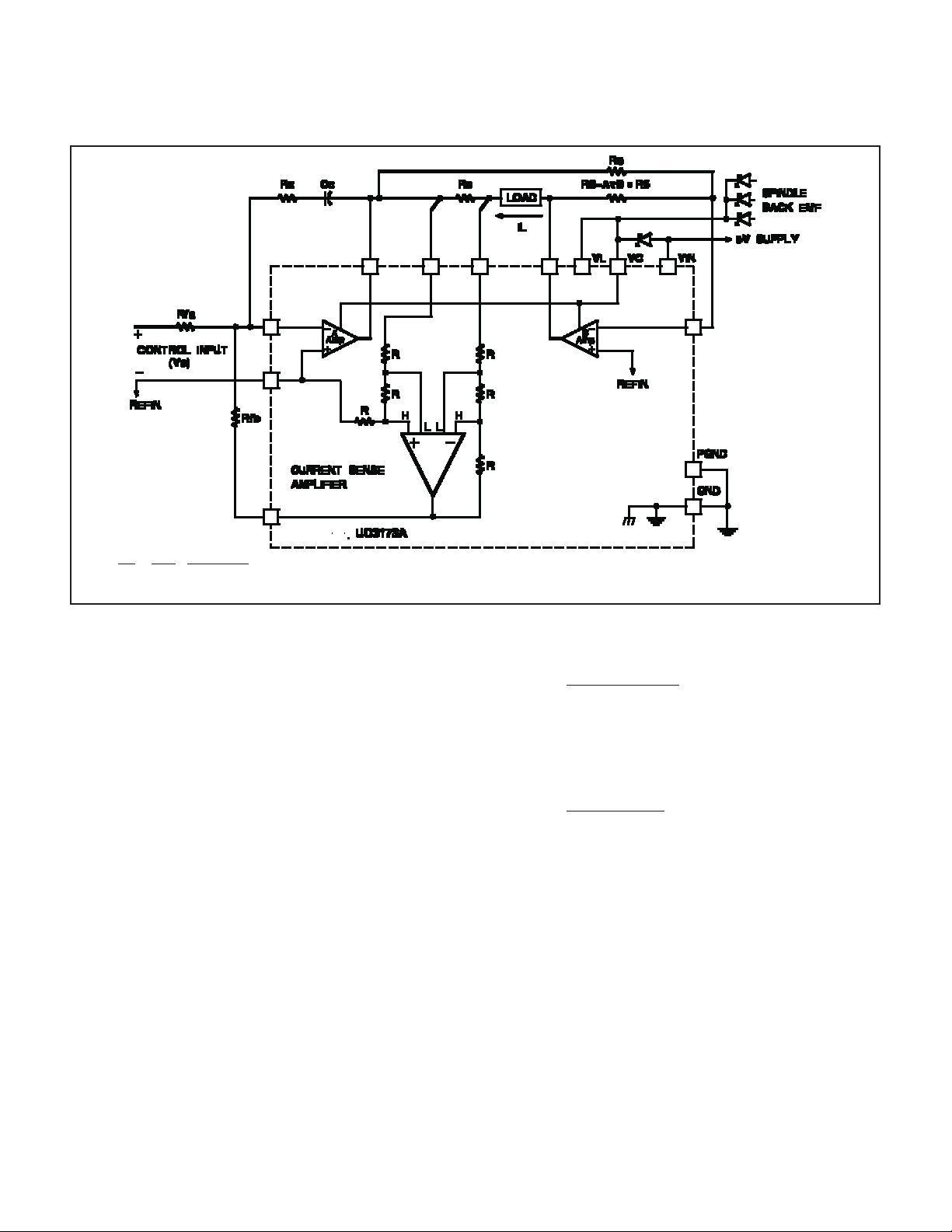
Figure 1. Typical application.
Design Procedure for Application of the UC3173A
The following is a simple design flow that can be used to
configure the UC3173A Full Bridge Power Amplifiers as
shown in Fig.1.
Definitions:
f
3DB
A
V
A
V
f
GBW
G
mHR
G
mLR
L = load inductance
R
L
A. Current Sense Resistor
Choose R
is the series current sense resistor.
B. Select Feedback Resistance
Choose a value of R
sense amplifier swing divided by 1mA. A value in the
range of 3k to 10k is suggested.
C. Set Transconductance
= the closed loop 3dB bandwidth
B = B amplifier closed loop gain, = R6/R5
CS = current sense amplifier gain, = 0.5 in high range,
and 2.0 in low range
A = gain bandwidth product of the A amplifier
= closed loop transconductance in high rangemode
= closed loop transconductance in low range mode
= load resistance
to be as large as head room will tolerate, this
S
to be less than the peak current
FB
UDG-94040
R=
FA
0.5 R G
R
FB
••
SmHR
(1)
If the range change option is not going to be used, it is
recommended that the device be set in the low range
mode and R
R=
FA be calculated by:
R
FA
FB
••
2R G
SmLR
(2)
D. Optimize Voltage Swing
In order to assure that maximum voltage drive to the
load is achievable, there are some precautions that
should be taken. In a standard configuration, the B amplifier is slaved to the A amplifier. The bias point of the
and the gain of the B amplifier, as well as the saturation
voltages of the power output stages, will affect the voltage available to the load.
There are two simple procedures to follow, either will
insure that the capabilities of the device are fully utilized.
The first is to set the REFIN voltage at the center of the
available voltage swing at the output of the power
amplifiers.This optimum reference is defined by
equation (3)
Calculate R
according to:
FA
8
Page 9

APPLICATION INFORMATION (cont.)
V (optimum)=
REFIN
Where:V
HS(SAT)
V
LS(SAT)
VIN- V + V
= high-side V
= low-side V
HS SAT LS SAT
() ()
2
at maximum load
SAT
at maximum load.
SAT
A second approach is to raise the gain of the B amplifier
to insure maximum swing. For a given REFIN voltage the
gain of the B amplifier, set by the ratio of the feedback
resistors, can be made greater than unity as given by:
VIN – V – V
AB=
V
V–V
REFIN
VIN – V – V
HS SAT
HS SAT
()
V–V
REFIN
LS SAT
()
()
REF
LS SAT
()
REF
or,
whichever is greater than unity.
For a typical case, where V
has been set at VIN/2,
REFIN
the required gain fora5voltsystem will be about 1.5,
and for a 12 volt system, 1.2.
It is worth noting that when using this method the B amplifier will saturate before the A amplifier on one polarity
of the voltage swing. During the time when the B amplifier is saturated and the A amplifier is not, the small signal bandwidth of the loop will be reduced by a factor of
(A
B + 1).
V
E. Loop Compensation
The normal configuration for compensation of the power
amplifier is shown in Fig. 1. A simple R
network, RCCC,
C
around the A amplifier is all that is required. The value of
the R
time constant is typically chosen to correspond
CCC
to the electrical time constant of the load, given by R
The bandwidth of the closed loop amplifier can be set by
choosing the value of R
2L f R
R=
C
Use A
V
A
CS = 2.0 if only the low range mode of operation is to
V
π• •
(1+ A B)A CS R
VV S
CS = 0.5 if range changing is to be used, and
. Calculate RCaccording to:
C
3dB FB
•
be used.
The compensation zero is typically set to coincide with
the L/R time constant of the Load. C
can then be calcu-
C
lated by:
C=
C
L
R(R +R)
CS L
In the closed loop transconductance amplifier, the A am-
(3)
(4)
/L.
L
(5)
(6)
UC3173A
plifier operates at the highest noise gain. Noise gain is a
measure of the feedback ratio at which the amplifier is
operating. For the configuration of the A amplifier in Fig.
1, the noise gain is given by the impedance ratio of the
R
and RFB. For the A amplifier to operate at its expected
closed loop gain, the noise gain at any frequency must
not exceed its Gain Bandwidth Product (GBW) divided
by that frequency. Applying this to the expression above
will yield a result for the maximum 3dB bandwidth that
can be achieved for a given configuration.
Where: f
In the UC3173A, to accommodate wider power amplifier
bandwidths, the GBW Product of the A amplifier has
been extended to 2MHz. Care should be taken that the
A amplifier gain bandwidth product is not limiting the
closed loop performance of the configured power amplifier. This is easily checked by making sure that R
less than a critical value, R
R=R
Again, use A
A
used.
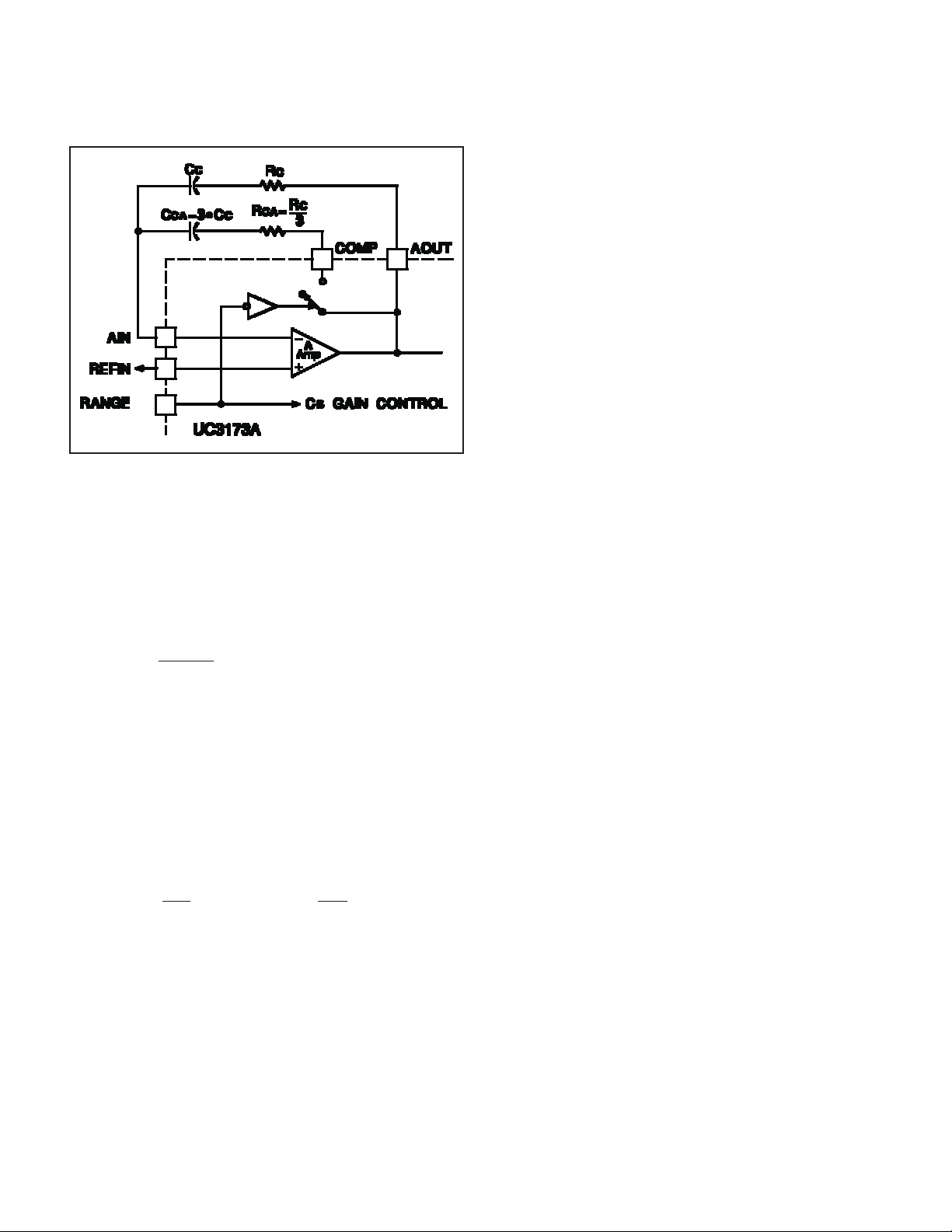
F. Using The Comp Pin
When the range change feature of the UC3173A is
used, the closed loop bandwidth of the power amplifier
will change according to (7). In other words, the bandwidth would be four times larger during the low range
mode when A
range mode when A
value of R
The COMP pin on the UC3173A can be used to do this.
The COMP pin acts as a simple switch that allows a parallel compensation network to be applied around the A
amplifier during low range operation. A simple network
as shown here will keep the loop response constant independent of the range condition.
To maintain the same 3dB bandwidth in both the high
and low range modes set R
series network, to the parallel combination of R
C-CC
f=
3dB MAX
()
fA(1+AB)ACSRR
C(MAX) FB
CS = 2.0 if only the low range mode of operation is
V
R=
CA
••••
GBW V V S FA
2L (R +R )
•
π
A is the GBW of the A amplifier.
GBW
(A B+1) A CS R (R +R )
CS = 0.5 if range changing is used, and
V
CS is equal to 2, than during the high
V
is adjusted to compensate.
C
R
C
,C =3C
3
FA FB
, as given by:
C(MAX)
fA2LR
VVSFAFB
CS is equal to 0.5, unless the
V
CA C
••
GBW FA
π
••
and CCAto:
CA
1
2
2
C
1
FA
(7)
(8)
(9)
is
9
Page 10
APPLICATION INFORMATION (cont.)
UDG-94041
The COMP pin switches in a parallel compensation
network to stabilize the small signal bandwidth with
range changes.
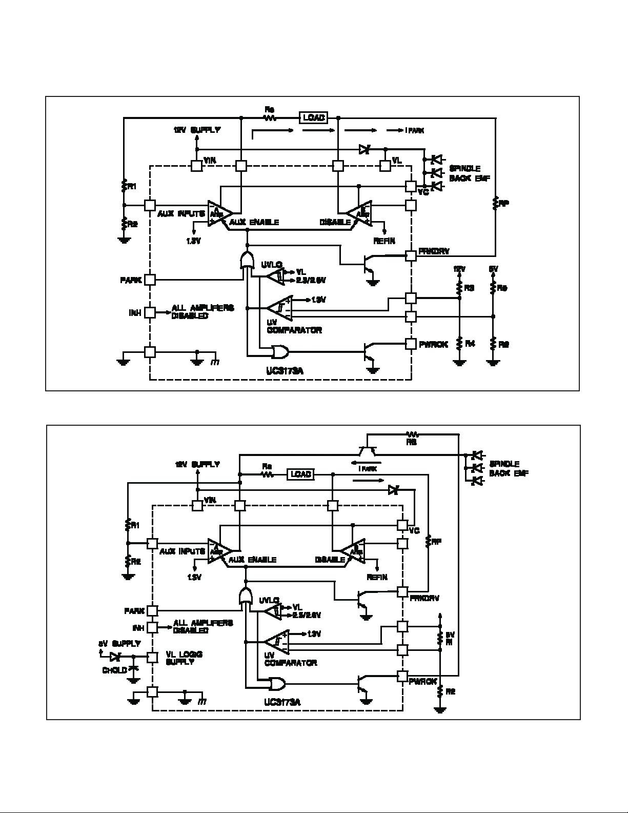
Head Parking
In Fig. 2, the UC3173A is shown configured to force a
programmed voltage at the A amplifier output upon the
activation of a park condition. A pair of feedback resistors
R1 and R2 set this voltage as defined by:
R1=R2
1.3
–1
VPARK
R2 is typically chosen in the range of 10kΩ to 100kΩ.
The B amplifier output is tri-stated during park, this side
of the load is driven low by the PRKDRV pin. A series resistor, RP in the figure, can be inserted in series with the
load to limit the peak current if required.
The UV thresholds for the supply monitors are set by
picking R4 and R6 values in the 10kΩ to 100kΩ range
and then calculating R3 and R5 according to:
R3 =R4
UV1
–1 ,andR5 =R6
1.3
UV2
1.3
–1
(10)
(11)
UC3173A
During park, supply to the load, and the UC3173A, is
typically recovered from the back EMF of the spindle
motor. When the supply voltage at the VL supply pin
drops below the UVLO voltage, (2.3V high-to-low), the
output of the A amplifier is forced high, over-riding the
programmed park voltage. The UC3173A will maintain
drive to the load down to low supply levels.For example,
with 1.5 volts of recovered back EMF, the UC3173A can
still deliver 50mA of drive to a 10Ω load.
Parking With Very Low Back EMF
The UC3173A can also be configured to get parking
drive to the load with very low recovered back EMF. Fig.
3 illustrates how the PWROK pin can be used to drive
an external PNP device to achieve very low parking
drive V
will be able to force approximately one volt across the
load with a recovered back EMF voltage of 1.3V.
During system commanded parking with the supplies
present, the VPARK pin is still used to set the maximum
voltage to the load. The logic function of the PWROK pin
is still available since the external PNP will provide isolation to this output when it is high.
Base drive to the PRKDRV and PWROK pins are provided by the VL supply pin. By using a hold up capacitor,
C
HOLD
back EMF drops to below 1V. A variation on this approach is to add a connection between the VL pin and
the recovered back EMF, this will eliminate the need for
the holdup capacitor and provide operation down to
about 1.2V of back EMF recovery. Care with this approach should be taken in case the 5V supply hangs at
just below the programmed UV threshold. In this situation large currents could flow from this supply through
the external PNP and into the A output which, until the
supply drops below a certain level, is forcing a programmed voltage.
losses. With this configuration, the UC3173A
SAT
, the drive can be maintained to the load as the
10
Page 11
UC3173A
Figure 2. Controlled velocity head parking.
UDG-94042
Figure 3. Head parking with low back EMF.
UNITRODE CORPORATION
7 CONTINENTAL BLVD. • MERRIMACK, NH 03054
TEL. (603) 424-2410 • FAX (603) 424-3460
UDG-94043
11
Page 12

IMPORTANT NOTICE
T exas Instruments and its subsidiaries (TI) reserve the right to make changes to their products or to discontinue
any product or service without notice, and advise customers to obtain the latest version of relevant information
to verify, before placing orders, that information being relied on is current and complete. All products are sold
subject to the terms and conditions of sale supplied at the time of order acknowledgement, including those
pertaining to warranty, patent infringement, and limitation of liability.
TI warrants performance of its semiconductor products to the specifications applicable at the time of sale in
accordance with TI’s standard warranty. Testing and other quality control techniques are utilized to the extent
TI deems necessary to support this warranty . Specific testing of all parameters of each device is not necessarily
performed, except those mandated by government requirements.
CERTAIN APPLICATIONS USING SEMICONDUCTOR PRODUCTS MAY INVOLVE POTENTIAL RISKS OF
DEATH, PERSONAL INJURY, OR SEVERE PROPERTY OR ENVIRONMENTAL DAMAGE (“CRITICAL
APPLICATIONS”). TI SEMICONDUCTOR PRODUCTS ARE NOT DESIGNED, AUTHORIZED, OR
WARRANTED TO BE SUITABLE FOR USE IN LIFE-SUPPORT DEVICES OR SYSTEMS OR OTHER
CRITICAL APPLICA TIONS. INCLUSION OF TI PRODUCTS IN SUCH APPLICATIONS IS UNDERST OOD TO
BE FULLY AT THE CUSTOMER’S RISK.
In order to minimize risks associated with the customer’s applications, adequate design and operating
safeguards must be provided by the customer to minimize inherent or procedural hazards.
TI assumes no liability for applications assistance or customer product design. TI does not warrant or represent
that any license, either express or implied, is granted under any patent right, copyright, mask work right, or other
intellectual property right of TI covering or relating to any combination, machine, or process in which such
semiconductor products or services might be or are used. TI’s publication of information regarding any third
party’s products or services does not constitute TI’s approval, warranty or endorsement thereof.
Copyright 1999, Texas Instruments Incorporated
 Loading...