

Page 1
The UC3717 has been designed to control and drive the current in
one winding of a bipolar stepper motor . The circuit consists of an LSTTL-compatible logic input, a current senso r, a monostable and an
output stage with built-in protection diodes. Two UC3717s and a few
external components form a complete control and drive unit for LSTTL or micro-proces sor contr o lled stepper motor system s.
The UC1717 is characterized for operation over the full military temperature range of -55°C to +125°C, the UC2717 is characterized for
-25°C to +85°C, and the UC3717 is characterized for 0°C to +70°C.
查询UC1717供应商
Stepper Motor Drive Circuit
FEATURES DESCRIPTION
• Half-step and Full-step Capability
• Bipolar Constant Current Motor Drive
• Built-in Fast Recovery Schottky
Commutating Diodes
• Wide Range of Current Control 5-1000mA
• Wide Voltage Range 10-45V
• Designed for Unregulated Motor Supply
Voltage
• Current Levels can be Selected in Steps
or Varied Continuously
• Thermal Overload Protectio n
ABSOLUTE MAXIMUM RATINGS (Not e 1)
Voltage
Logic Supply, V
Output Supply, V
Input Voltage
Logic Inputs (Pins 7, 8, 9). . . . . . . . . . . . . . . . . . . . . . . . . . . . . . . . . . 6V
Analog Input (Pin 10) . . . . . . . . . . . . . . . . . . . . . . . . . . . . . . . . . . . . Vcc
Reference I nput (Pin 11) . . . . . . . . . . . . . . . . . . . . . . . . . . . . . . . . . 15V
Input Current
Logic Inputs (Pins 7, 8, 9) . . . . . . . . . . . . . . . . . . . . . . . . . . . . . . . -10mA
Analog Inputs (Pins 10, 11). . . . . . . . . . . . . . . . . . . . . . . . . . . . . . -10mA
Output Current (Pins 1, 15) . . . . . . . . . . . . . . . . . . . . . . . . . . . . . . . . ±1A
Junction Temperature, T
Storage Temperature Range, T
CC . . . . . . . . . . . . . . . . . . . . . . . . . . . . . . . . . . . . . . . 7V
M . . . . . . . . . . . . . . . . . . . . . . . . . . . . . . . . . . . . . . 45V
J. . . . . . . . . . . . . . . . . . . . . . . . . . . . . . . +150°C
S . . . . . . . . . . . . . . . . . . -55°C to +150°C
UC1717
UC2717
UC3717
Note 1: All voltages are with respect to ground, Pins
4,5, 12, 13. Pin num ber s refe r to DIL-16 packa ge. Currents are positive int o, negat ive ou t of the spe cified terminal.
Note 2: Consult Packaging Sect ion of Databook for information on thermal l imitat ions and considerations of
package.
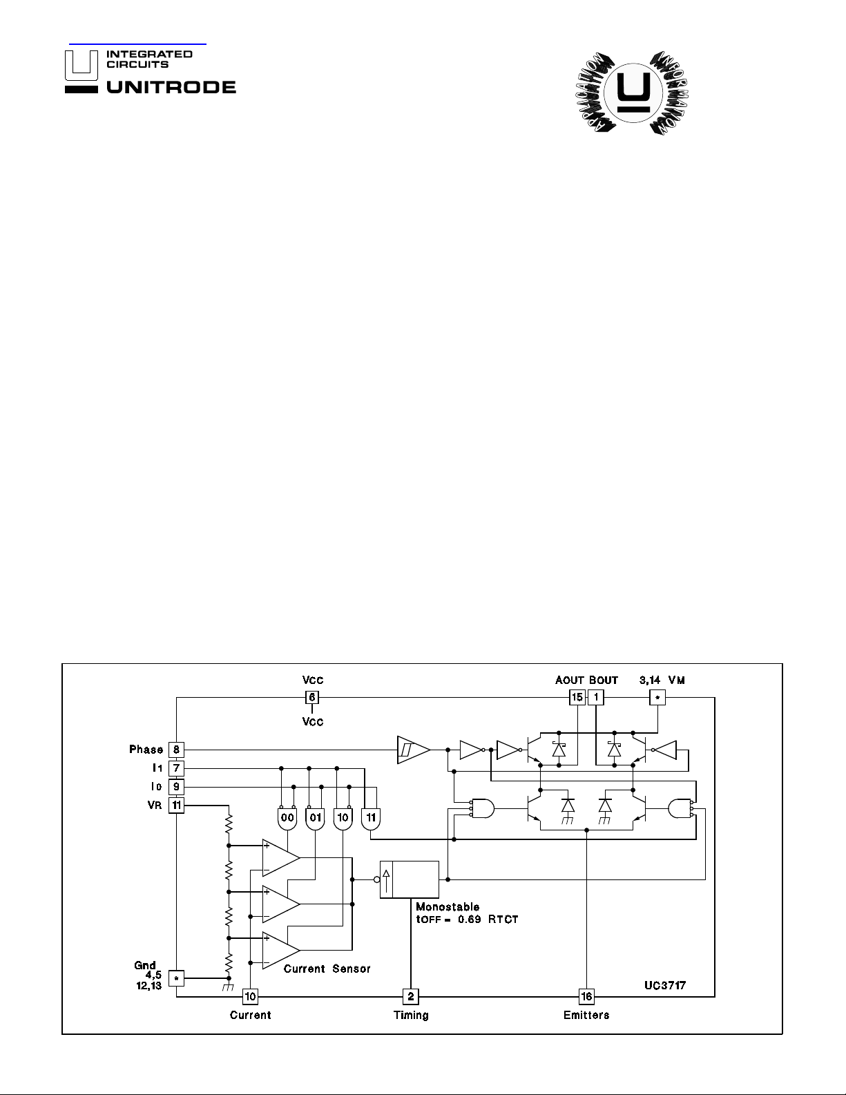
BLOCK DIAGRAM
7/95
Page 2
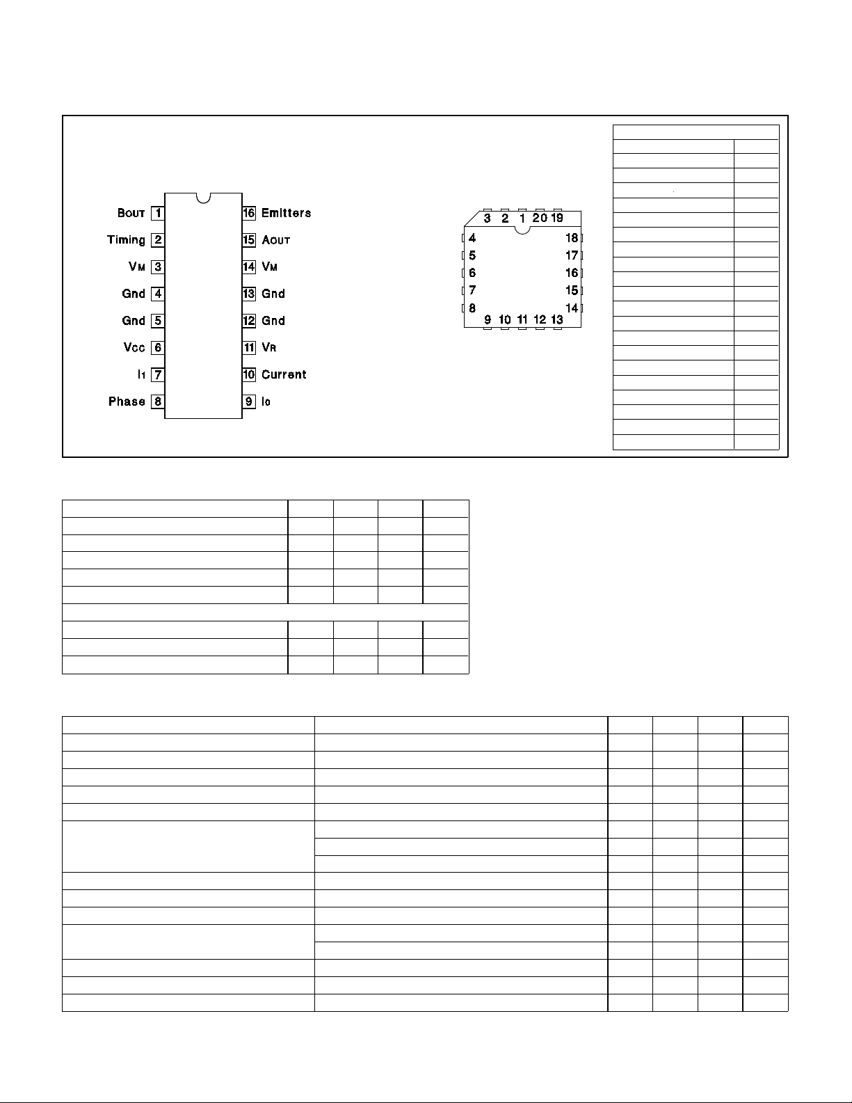
CONNECTION DIAG RAMS
Unless otherwise specified, these specifications apply for VCC = 5V, TA = TJ .
UC1717
UC2717
UC3717
DIL-16 (TOP VI EW)
J or N Package
RECOMMENDED OPERATING CONDITIONS
PARAMETER MIN TYP MAX UNITS
Supply Voltage, V
Supply Voltage, V
Output Current. I
Rise Time Logic Inputs, t
Fall Time Logic Inputs, t
Ambient Temperature, T
UC1717 -55 125 °C
UC2717 -25 85 °C
UC3717 0 70 °C
CC 4.75 5 5.25 V
M 10 40 V
M 20 800 mA
R 2 µs
F 2 µs
A
PLCC-20 (TOP VIEW)
Q Package
PACKAGE PIN FUNCTION
FUNCTION PIN
N/C
BOUT 2
Timing 3
VM 4
Gnd 5
N/C 6
Gnd 7
VCC 8
I1 9
Phase 10
N/C 11
I0 12
Current 13
VR 14
Gnd 15
N/C 16
Gnd 17
Vm 18
AOUT 19
Emitters 20
1
ELECTRICAL CHARACTERIST ICS
PARAMETER TEST CONDITIONS MIN TYP MAX UNITS
Supply Curren t, I
High-Level Input Voltage, Pins 7, 8, 9 2.0 V
Low-Level I nput Voltage, Pins 7, 8, 9 0.8 V
High-Level Input Current , Pins 7, 8, 9 V
Low Level Input Curre nt, Pins 7, 8, 9 V
Compara tor Thresh old Volta ge I
Compara to r Input Cur ren t -20 20 µA
Output Leakage Current I
Total Saturation Voltage Drop I
Total Power Dissipation I
Cut Off Time, t
Turn Off Delay, t
Thermal Shutd own Jun ctio n Tem per atur e +160 +180 ° C
CC 25 mA
I = 2.4V 20 µA
I = 0.4V -0.4 mA
O = 0, I1 = 0, VR = 5.0V 390 420 440 mV
I
O = 1, I1 = 0, VR = 5.0V 230 250 270 mV
I
O = 0, I1 = 1, VR = 5.0V 65 80 90 mV
O = 1, I1 = 1, TA = +25°C 100 µA
M = 500mA 4.0 V
M = 500mA, fS = 30kHz 1.4 2.1 W
I
M = 800mA, fS = 30kHz 2.9 3.1 W
OFF VM = 10 V, tON≥ 5µs (See Figure 5 and 6) 25 30 35 µs
D TA = +25°C; dVc/dt ≥ 50mV/µs (See Figure 5 and 6) 1.6 2 .0 µs
2
Page 3
UC1717
UC2717
UC3717
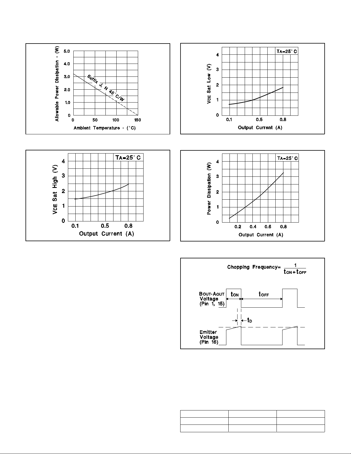
Figure 1
Figure 2: Ty pical Sour ce Satur at ion Voltage vs Outp ut Curr ent
FUNCTIONAL DESCRI PT IO N
The UC3717 drive circuit shown in the block diagram includes the following functions:
(1) Phase Logic and H-Bridge Output Stage
(2) V o ltag e D i v id er w i t h t h r e e C o m p a r a t ors f o r cur r e n t cont r o l
(3) Tw o Logic inputs for Digit al current lev el selec t
(4) Monostable for off time ge nerat ion
Figure 3: Ty pical Sink Sat ura tion Voltage vs Outpu t Cur rent
Figure 4: Typical Power Losse s vs Output Cur ren t
Input Logic: If any of the logic inputs are left open, the
circuit will treat it as a high level input.
Phase Input: The phase input terminal, pin 18, controls
the direction of the current through the motor winding.
The Schmidt-Trigger input coupled with a fixed time delay assures noise immunity and eliminates cross conduction in the output stage during phase changes. A low
level on the phase input will turn Q2 on and enable Q3
while a high level wi ll turn Q1 on and enable Q4. (See
Figure 7).
Output Stage: The output stage consists of four Darlington transistors and associated diodes connected in
an H-Bridge configuration. The diodes are needed to provide a current path when the transistors are being
switched. For fast recovery, Schottky diodes are used
Figure 5: Connections and Compone nt Values as in Figure 6.
across the source transistors. The Schottky diodes allow
the current to circulate through the winding while the sink
transistors are being switched off. The diodes across the
sink transistors in conjuncti on with the Schottkys provide
the path for the decaying current during phase reversal.
(See Figure 7).
PHASE INPUT Q1, Q4 Q2, Q3
Low Off On
High On Off
3
Page 4

UC1717
UC2717
UC3717
I0 I1 CURRENT LEVEL
0 0 100%
1 0 60%
0 1 19%
1 1 Curr ent Inhi bit
Current Control: The voltage divider, comparators and
monostable provide a means for current sensing and
control. The two bit input (I
0, I1) logic selects the desired
comparator. The monostable controls the off time and
therefore the magnitude of the current decrease. The
time duration is determined by R
T and CT connected to
the timing termina l (pin 2). The referen ce terminal (pin
11) provides a means of continuou sly varying the cur-
rent for situations requiring half-stepping and microstepping. The relationship between the logic input
signals at pin 7 and 9 in reference to the current level is
shown in Table 1. The values of the different current levels are determined by the reference voltage together
with the value of the external sense resistor R
S (pin 16).
Single-Pulse Generator: The pulse generator is a
monostable triggered on the positive going edge of the
comparator. Its output is high during the pulse time and
this pulse switches off the power feed to the motor wind-
Figure 6
ing causing the current to decay . The time is determined
by the external timing components R
T
OFF
= 0.69 RTC
T and CT as:
T
If a new trigger signal should occur during TOFF, it is ig-
nored.
Note: Dashed lines indicat e current decay paths.
Figure 7: Sim pl ified Schemat ic of Outpu t Stage
4
Page 5

FUNCTIONAL DESCRI PT IO N (con t. )
Overload Protection: The circuit is equipped with a
thermal shutdown function, which will limit the junction
temperature by reducing the output current. It should be
noted however, that a short circuit of the output is not
permitted.
Operation: When the voltage is applied across the motor
winding the current rises linearly and appears across the
external sense resistor as an analog voltage. This voltage is fed through a low pass filter R
comparator (pin 10). At the moment the voltage rises beyond the comparator threshold voltage the monostable is
triggered and its output turns off the sink transistors. The
current then ci rculates through the source transistor and
the appropriate Scho ttky diode. After the one shot has
timed out, the sink transistsor i s turned on again and the
procedure repe ated until a curren t reverse command is
given. By reversing the logic level of the phase input (pin
8), both active transistors are being turned off and the
opposite pair turne d on. When this happ ens the current
must first deca y to zero before it can reverse. The current path then provided is through the two diodes and the
power-supply. Refer to Figure 7. It should be noted at
this time that the slope of the current decay is steeper,
and this is due to the higher vol tage build up across the
winding. For better speed performance of the stepping
motor at half step mode, the phase logi c level should be
changed at the same time the current inhibit is applied. A
typical current wave form is shown in Figure 8.
C, CC to the voltage
UC1717
UC2717
UC3717
Figure 9
Figure 8
APPLIC AT IO NS
A typical chopper drive for a two phase bipolar permanent magnet or hybrid stepping motor is shown in Figure
9. The input can be controlled by a microprocessor, TTL,
LS or CMOS logic.
The timing di agra m in Figu re 1 0 sh ows the required signal input for a two phase, full step, stepping sequence.
Figure 11 shows a one phase, full step, stepping sequence, commonly re ferred to as wave drive. Figure 12
shows the required input signal for a one phase-two
phase stepping sequence called half-stepping.
The circuit of Figure 13 provides the signal shown in Figure 10, a nd in conjunction with the circuit shown in Figure 9, will implement a pulse-to-step two phase, full step,
bidirectional motor drive.
The schematic of Figure 14 shows a pulse to half step
circuit generating the signal shown in Figure 12. Care
has been taken to change the phase signal the same
time the current inhibit is applied. This will allow the current to decay faster and therefore enhance the motor
performance at higher step rates.
Using the UC3717 to dri ve the L298 provides a uniquely
packaged state-of-the-art high power stepper motor control and drive. See Figure 15.
5
Page 6

FUNCTIONAL DESCRI PT IO N (con t. )
Figure 10: Phase Input Signal for Two Phase Fu ll Step Drive (4 Step Seque nce)
UC1717
UC2717
UC3717
Figure 11: Phase and Curren t-I nhibit Signal for W ave Drive (4 Step Sequence)
Figure 12: Phase and Cur ren t-I nhibit Signal for Half Stepp in g (8 Step Seq uenc e)
Figure 13: Fu ll Step Bidirec tion al Two Phase Drive Log ic
6
Page 7

UC1717
UC2717
UC3717
Figure 14: Half-Step, Bidirectiona l Driv e Logic
CONSIDERATI ON
Half-Steppin g : In the half step sequence the powe r in-
put to the motor alternates between one or two phases
being energized. In a two phase motor the electrical
phase shift between the windings is 90 degrees. The
torque developed is the vector sum of the two windings
energized. Therefore when only one winding is energized
the torque of the motor is reduced by approximately
30%. This causes a torque ripple and if it is necessary to
compensate for this, the V
the current of the single energized winding.
Ramping: Every drive system has inertia and must be
considered in the drive scheme. The rotor and load inertia plays a big role at higher speeds. Unlike the DC motor
the stepping motor is a synchronous motor and does not
change its speed due to load variations. Examining typical stepping motors, torque vs . speed curves indicates a
sharp torque drop off for the start-stop without error
curve, even with a constant current drive. The reason for
this is that the torque requirements increase by the
square of the speed change, and the power need increases by the cube of the speed change. As it can be
seen, for good motor performance controlled acceleration and deceleration should be considered.
Iron Core Losses: Some motors, especially the Tin-Can
type, exhibit high iron losses mostly due to eddy currents
input can be used to boost
R
which rise in an exponential manner as the frequency or
step rate is increased . The power l osses ca n not be calculated by I
2
R where I is the chopping current level and
R the DC resistance of the coil. Actual measurements indicate the effective resistance may be many times larger.
Therefore, for 100% duty cycle the current must be limited to a value which will not overheat the motor. This
may not be necessary for lower duty cycle operation.
Interference: Electrical noise generated by the chopping
action can cause interference problems, particularly in
the vicinity of magnetic storage media. With this in mind,
printed circuit layouts, wire runs and decoupling must be
considered. 0.01 to 0.1µF ceramic capacitors for high frequency bypass located near the drive package across
V+ and ground might be very helpful. The connection
and ground leads of the current sensing components
should be kept as short as possible.
Ordering Information
UNITRODE TYPE N UM BER
UC3717N - 16 Pin Dual-in-line (DIL) "Bat Wing" Package
UC1717J - 16 Pin Dual-in-line Ceramic Package
UC1717SP - 16 Pin Dual-in - line He rmeti c Power P ackage
7
Page 8

UC1717
UC2717
UC3717
UNITRODE INTEGRATED CIRCUITS
7 CONTINENTAL BLVD. • MERRIMACK, NH 03054
TEL. (603) 424-2410 • FAX (603)424-3460
Figure 15: UC3 717 wi th L29 8 Pow er Ampl ifi er
8
Page 9

IMPORTANT NOTICE
T exas Instruments and its subsidiaries (TI) reserve the right to make changes to their products or to discontinue
any product or service without notice, and advise customers to obtain the latest version of relevant information
to verify, before placing orders, that information being relied on is current and complete. All products are sold
subject to the terms and conditions of sale supplied at the time of order acknowledgement, including those
pertaining to warranty, patent infringement, and limitation of liability.
TI warrants performance of its semiconductor products to the specifications applicable at the time of sale in
accordance with TI’s standard warranty. Testing and other quality control techniques are utilized to the extent
TI deems necessary to support this warranty . Specific testing of all parameters of each device is not necessarily
performed, except those mandated by government requirements.
CERTAIN APPLICA TIONS USING SEMICONDUCT OR PRODUCTS MAY INVOLVE POTENTIAL RISKS OF
DEATH, PERSONAL INJURY, OR SEVERE PROPERTY OR ENVIRONMENTAL DAMAGE (“CRITICAL
APPLICATIONS”). TI SEMICONDUCTOR PRODUCTS ARE NOT DESIGNED, AUTHORIZED, OR
WARRANTED TO BE SUITABLE FOR USE IN LIFE-SUPPORT DEVICES OR SYSTEMS OR OTHER
CRITICAL APPLICA TIONS. INCLUSION OF TI PRODUCTS IN SUCH APPLICATIONS IS UNDERST OOD TO
BE FULLY AT THE CUSTOMER’S RISK.
In order to minimize risks associated with the customer’s applications, adequate design and operating
safeguards must be provided by the customer to minimize inherent or procedural hazards.
TI assumes no liability for applications assistance or customer product design. TI does not warrant or represent
that any license, either express or implied, is granted under any patent right, copyright, mask work right, or other
intellectual property right of TI covering or relating to any combination, machine, or process in which such
semiconductor products or services might be or are used. TI’s publication of information regarding any third
party’s products or services does not constitute TI’s approval, warranty or endorsement thereof.
Copyright 1999, Texas Instruments Incorporated
 Loading...