

Page 1
查询5962-0051401QEA供应商
Dual Non-Inverting Power Driver
FEATURES DESCRIPTION
3.0A Peak Current Totem Pole
•
Output
5 to 35V Operation
•
25ns Rise and Fall Times
•
25ns Propagation Delays
•
Thermal Shutdown and Under-
•
Voltage Protection
High-Speed, Power MOSFET
•
Compatible
Efficient High Frequency Operation
•
Low Cross-Conduction Current
•
Spike
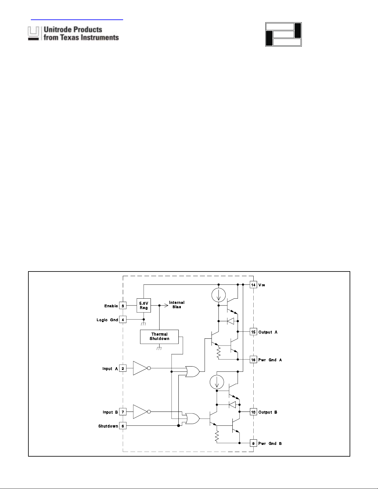
The UC1708 family of power drivers is made with a high-speed,
high-voltage, Schottky process to interface control functions and high-power
switching devices – particularly power MOSFETs. Operating over a 5 to 35
volt supply range, these devices contain two independent channels. The A
and B inputs are compatible with TTL and CMOS logic families, but can
withstand input voltages as high as V
to 3A as long as power dissipation limits are not exceeded.
Although each output can be activated independently with its own inputs,
they can be forced low in common through the action of either a digital high
signal at the Shutdown terminal or by forcing the Enable terminal low. The
Shutdown terminal will only force the outputs low, it will not effect the behav
ior of the rest of the device.The Enable terminal effectively places the device
in under-voltage lockout, reducing power consumption by as much as 90%.
During under-voltage and disable (Enable terminal forced low) conditions,
the outputs are held in a self-biasing, low-voltage, state.
application
INFO
available
IN. Each output can source or sink up
UC1708
UC2708
UC3708
-
• Enable and Shutdown Functions
• Wide Input Voltage Range
• ESD Protection to 2kV
BLOCK DIAGRAM
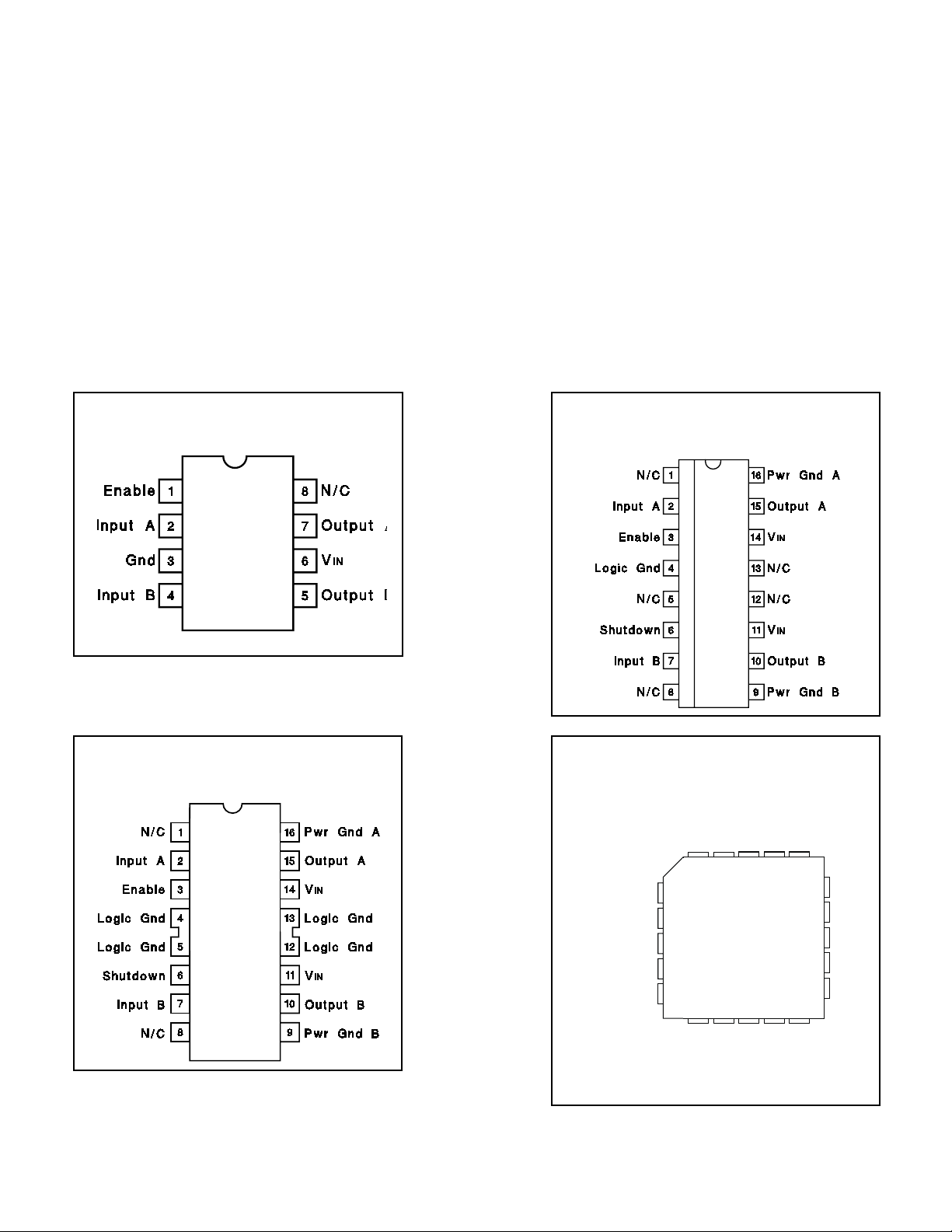
The UC3708 and UC2708 are available in plastic 8-pin MINI DIP and 16-pin
“bat-wing” DIP packages for commercial operation over a 0
perature range and industrial temperature range of -25
respectively. For operation over a -55
UC1708 is available in hermetically sealed 8-pin MINI CDIP, 16 pin CDIP
and 20 pin CLCC packages.Surface mount devices are also available.
o
C to +125oC temperature range, the
o
Cto+70oC tem-
o
Cto+85oC
Note: Shutdown feature is not available in J or N packages only.
SLUS171A - MARCH 1997 - REVISED AUGUST 2001
UDG-92024-1
Page 2
UC1708
UC2708
UC3708
ABSOLUTE MAXIMUM RATINGS (Note 1)
Supply Voltage VIN . . . . . . . . . . . . . . . . . . . . . . . . . . . . . . . . . . . . . . . . . . . . . . . . . . . . . . . . . . . . . . . . . . . . . . . . . . . . . . . . . . . . 35V
Output Current (Each Output, Source or Sink)
Steady-State . . . . . . . . . . . . . . . . . . . . . . . . . . . . . . . . . . . . . . . . . . . . . . . . . . . . . . . . . . . . . . . . . . . . . . . . . . . . . . . . . . . . . . 0.5A
Peak Transient . . . . . . . . . . . . . . . . . . . . . . . . . . . . . . . . . . . . . . . . . . . . . . . . . . . . . . . . . . . . . . . . . . . . . . . . . . . . . . . . . . . . . . 3A
Ouput Voltage . . . . . . . . . . . . . . . . . . . . . . . . . . . . . . . . . . . . . . . . . . . . . . . . . . . . . . . . . . . . . . . . . . . . . . . . . . .
Enable and Shutdown Inputs . . . . . . . . . . . . . . . . . . . . . . . . . . . . . . . . . . . . . . . . . . . . . . . . . . . . . . . . . . . . . . . . . . . . . .
A and B Inputs . . . . . . . . . . . . . . . . . . . . . . . . . . . . . . . . . . . . . . . . . . . . . . . . . . . . . . . . . . . . . . . . . . . . . . . . . . .
Operating Junction Temperature (Note 2) . . . . . . . . . . . . . . . . . . . . . . . . . . . . . . . . . . . . . . . . . . . . . . . . . . . . . . . . . . . . . . . . 150°C
Storage Temperature Range. . . . . . . . . . . . . . . . . . . . . . . . . . . . . . . . . . . . . . . . . . . . . . . . . . . . . . . . . . . . . . . . . . . . . -65° to 150°C
Lead Temperature (Soldering, 10 Seconds). . . . . . . . . . . . . . . . . . . . . . . . . . . . . . . . . . . . . . . . . . . . . . . . . . . . . . . . . . . . . . . 300°C
-0.3 to (VIN + 0.3)V
-0.3 to 6.2V
-0.3 to (VIN + 0.3)V
NOTE 1: All voltages are with respect to Logic Gnd pin.All currents are positive into, negative out of, device terminals.
NOTE 2:Consult Unitrode Integrated Circuits databook for information regarding thermal specifications and limitations of packages.
CONNECTION DIAGRAMS
DIL-8 (Top View)
J Or N Package
DIL-16 (Top View)
JE or NE Package
SOIC-16 (Top View)
DW Package
CLCC-20 (Top View)
L Package
INPUT A
N/C
N/C
PWR GND A
OUTPUT A
Note: In JE package Pin 4 is logic ground. Pins 5, 12,
and 13 are N/C.
N/C
N/C
20 19
PWR GND B
18
17
16
15
14
OUTPUT B
VIN
N/C
N/C
N/C
VIN
ENABLE
LOGIC GND
N/C 6
N/C
SHUTDOWN
321
4
5
7
8
910111213
INPUT B
2
Page 3
UC1708
UC2708
UC3708
ELECTRICAL CHARACTERISTICS: Unless otherwise stated, V
for: –55
o
C<TA<125oC for the UC1708, –25oC<TA<+85oC for the UC2708, and 0oC<TA<70oC for the UC3708.TA =TJ.
=10V to 35V, and these specifications apply
IN
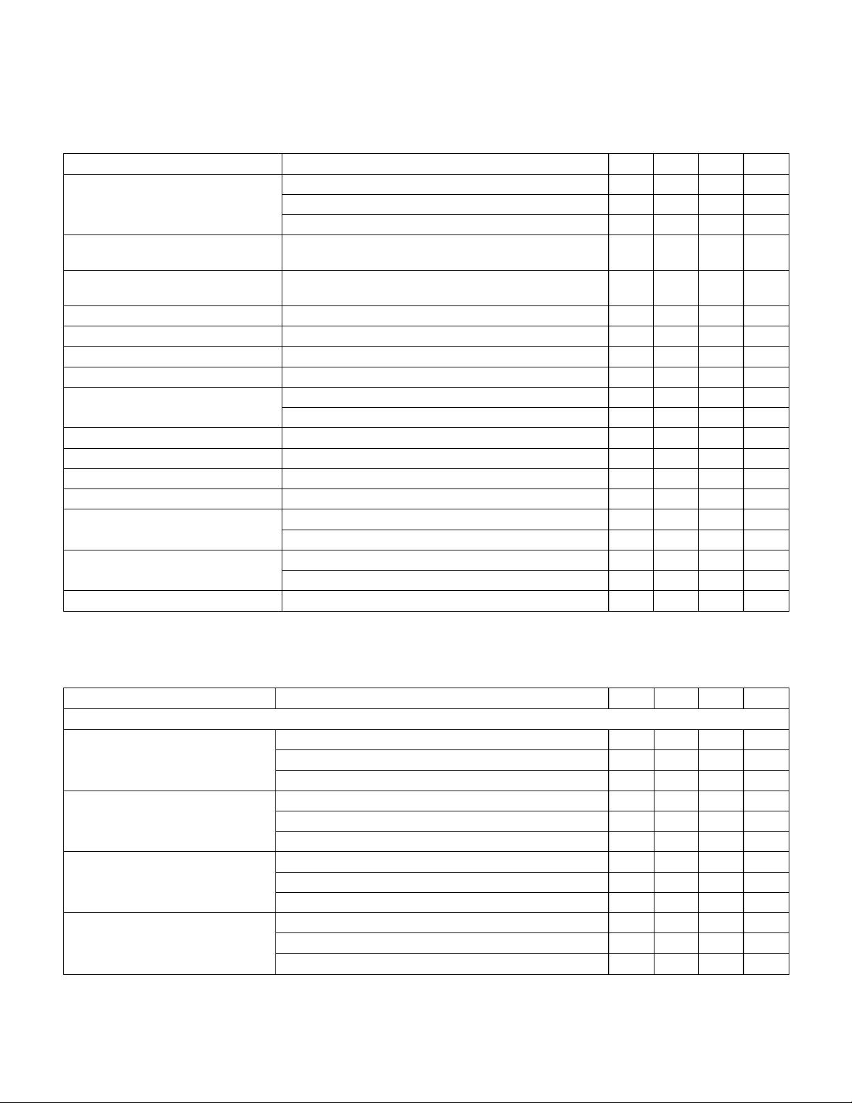
PARAMETER TEST CONDITIONS MIN TYP MAX UNITS
IN Supply Current OutputsLow 18 26 mA
V
Outputs High 14 18 mA
Enable = 0V 1 4 mA
A, B and Shutdown Inputs Low
0.8 V
Level
A, B and Shutdown Inputs High
2.0 V
Level
A, B Input Current Low V
A, B Input Current High V
A, B Input Leakage Current High V
Shutdown Input Current Low V
Shutdown Input Current High V
Enable Input Current Low V
Enable Input Current High V
A,B = 0.4V -1 -0.6 mA
A,B = 2.4V -200 50 µA
A,B = 35.3V 200 µA
SHUTDOWN = 0.4V 20 100 µA
SHUTDOWN = 2.4V 170 500 µA
SHUTDOWN = 6.2V 0.6 1.5 mA
V
ENABLE = 0V -600 -460 200 µA
ENABLE = 6.2V 200 µA
Enable Threshold Rising 2.8 3.6 V
Enable Threshold Falling 1.0 2.4 3.4 V
Output High Sat., V
Output Low Sat., V
IN -VOUT IOUT = -50mA 2.0 V
OUT = -500mA 2.5 V
I
OUT IOUT = 50mA 0.5 V
OUT = 500mA 2.5 V
I
Thermal Shutdown 155 °C
SWITCHING CHARACTERISTICS (Figure 1), (VIN = 20V, delays measured to 10% output change.)
PARAMETER TEST CONDITIONS MIN TYP MAX UNITS
From A,B Input to Output:
Rise Time Delay (TPLH) CL = 0pF 25 40 ns
CL = 1000pF (Note 3) 25 40 ns
CL = 2200pF 30 45 ns
10% to 90% Rise (TTLH) CL = 0pF 55 75 ns
CL = 1000pF (Note 3) 25 50 ns
CL = 2200pF 40 55 ns
Fall Time Delay (TPHL) CL = 0pF 25 40 ns
CL = 1000pF (Note 3) 25 45 ns
CL = 2200pF 35 50 ns
90% to 10% Fall (TTHL) CL = 0pF 15 20 ns
CL = 1000pF (Note 3) 25 45 ns
CL = 2200pF 40 55 ns
NOTE 3: These parameters, specified at 1000pF, although ensured over recommended operating conditions, are not tested in
production.
3
Page 4
UC1708
UC2708
UC3708
SWITCHING CHARACTERISTICS (Figure 1), (VIN = 20V, delays measured to 10% output change.)
From Shutdown Input to Output
Rise Time Delay (TPLH) CL = 0pF 25 75 ns
CL = 1000pF (Note 3) 30 75 ns
CL = 2200pF 35 75 ns
10% to 90% Rise (TTLH) CL = 0pf 50 75 ns
CL = 1000pF (Note 3) 25 50 ns
CL = 2200pF 40 55 ns
Fall Time Delay (TPHL) CL = 0pF 25 45 ns
CL = 1000pF (Note 3) 30 50 ns
CL = 2200pF 35 55 ns
90% to 10% Fall (TTHL) CL = 0pF 25 20 ns
CL = 1000pF (Note 3) 25 45 ns
CL = 2200pF 40 55 ns
Total Supply Current F = 200kHz, 50% duty cycle, both channels; CL = 0pF 23 25 mA
F = 200kHz, 50% duty cycle, both channels; CL = 2200pF 38 45 mA
NOTE 3: These parameters, specified at 1000pF, although ensured over recommended operating conditions, are not tested in
production.
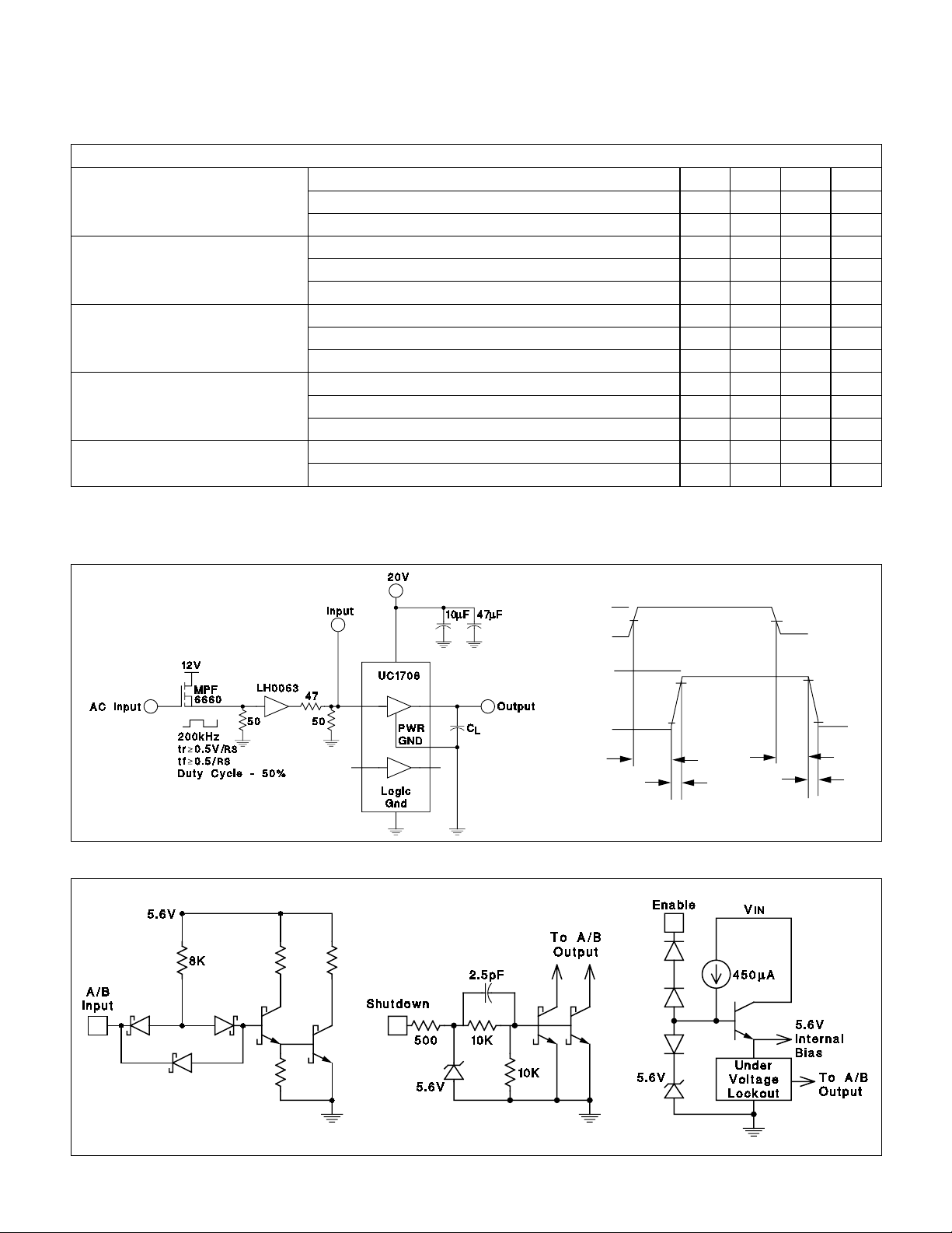
Figure 1: AC Test Circuit and Switching Time Waveforms
Figure 2: Equivalent Input Circuits
4.3V
INPUT
OUTPUT
TP
0V
20V
0V
LH
50%
90%
10%
TP
HL
TT
LH
50%
90%
10%
TT
HL
UDG-92026
Note: Shutdown feature available only in JE, NE or DW Packages.
UDG-92025
4
Page 5
PACKAGE OPTION ADDENDUM
www.ti.com
PACKAGING INFORMATION
Orderable Device Status
5962-0051401Q2A ACTIVE LCCC FK 20 1 TBD POST-PLATE Level-NC-NC-NC
5962-0051401QEA ACTIVE CDIP J 16 1 TBD A42 SNPB Level-NC-NC-NC
5962-0051401QPA ACTIVE CDIP JG 8 1 TBD A42 SNPB Level-NC-NC-NC
5962-0051401V2A ACTIVE LCCC FK 20 1 TBD Call TI Level-NC-NC-NC
5962-0051401VEA ACTIVE CDIP J 16 1 TBD Call TI Level-NC-NC-NC
5962-0051401VPA ACTIVE CDIP JG 8 1 TBD A42 Level-NC-NC-NC
UC1708J ACTIVE CDIP JG 8 1 TBD A42 SNPB Level-NC-NC-NC
UC1708J883B ACTIVE CDIP JG 8 1 TBD A42 SNPB Level-NC-NC-NC
UC1708JE ACTIVE CDIP J 16 1 TBD A42 SNPB Level-NC-NC-NC
UC1708JE883B ACTIVE CDIP J 16 1 TBD A42 SNPB Level-NC-NC-NC
UC1708L883B ACTIVE LCCC FK 20 1 TBD POST-PLATE Level-NC-NC-NC
UC2708D OBSOLETE UTR TBD Call TI Call TI
UC2708DW ACTIVE SOIC DW 16 40 Green (RoHS &
UC2708DWG4 ACTIVE SOIC DW 16 40 Green (RoHS &
UC2708DWTR ACTIVE SOIC DW 16 2000 Green(RoHS &
UC2708DWTRG4 ACTIVE SOIC DW 16 2000 Green (RoHS &
UC2708J OBSOLETE UTR TBD Call TI Call TI
UC2708JE OBSOLETE UTR TBD Call TI Call TI
UC2708N ACTIVE PDIP P 8 50 Green (RoHS &
UC2708NE ACTIVE PDIP N 16 25 Green (RoHS &
UC2708NG4 ACTIVE PDIP P 8 50 Green (RoHS &
UC2708Q OBSOLETE UTR TBD Call TI Call TI
UC3708DW ACTIVE SOIC DW 16 40 Green (RoHS &
UC3708DWG4 ACTIVE SOIC DW 16 40 Green (RoHS &
UC3708DWTR ACTIVE SOIC DW 16 2000 Green(RoHS &
UC3708DWTRG4 ACTIVE SOIC DW 16 2000 Green (RoHS &
UC3708J ACTIVE CDIP JG 8 1 TBD A42 SNPB Level-NC-NC-NC
UC3708JE ACTIVE CDIP J 16 1 TBD A42 SNPB Level-NC-NC-NC
UC3708N ACTIVE PDIP P 8 50 Green (RoHS &
UC3708NE ACTIVE PDIP N 16 25 Green (RoHS &
UC3708NEG4 ACTIVE PDIP N 16 25 Green (RoHS &
UC3708NG4 ACTIVE PDIP P 8 50 Green (RoHS & CU NIPDAU Level-NC-NC-NC
(1)
Package
Type
Package
Drawing
Pins Package
Qty
Eco Plan
no Sb/Br)
no Sb/Br)
no Sb/Br)
no Sb/Br)
no Sb/Br)
no Sb/Br)
no Sb/Br)
no Sb/Br)
no Sb/Br)
no Sb/Br)
no Sb/Br)
no Sb/Br)
no Sb/Br)
no Sb/Br)
(2)
Lead/Ball Finish MSL Peak Temp
CU NIPDAU Level-2-260C-1YEAR
CU NIPDAU Level-2-260C-1YEAR
CU NIPDAU Level-2-260C-1YEAR
CU NIPDAU Level-2-260C-1YEAR
CU NIPDAU Level-NC-NC-NC
Call TI Level-NC-NC-NC
CU NIPDAU Level-NC-NC-NC
CU NIPDAU Level-2-260C-1YEAR
CU NIPDAU Level-2-260C-1YEAR
CU NIPDAU Level-2-260C-1YEAR
CU NIPDAU Level-2-260C-1YEAR
CU NIPDAU Level-NC-NC-NC
Call TI Level-NC-NC-NC
Call TI Level-NC-NC-NC
4-Nov-2005
(3)
Addendum-Page 1
Page 6

PACKAGE OPTION ADDENDUM
www.ti.com
Orderable Device Status
(1)
Package
Type
Package
Drawing
Pins Package
Qty
Eco Plan
(2)
Lead/Ball Finish MSL Peak Temp
4-Nov-2005
(3)
no Sb/Br)
UC3708Q OBSOLETE UTR TBD Call TI Call TI
(1)
The marketing status values are defined as follows:
ACTIVE: Product device recommended for new designs.
LIFEBUY: TI has announced that the device will be discontinued, and a lifetime-buy period is in effect.
NRND: Not recommended for new designs. Device is in production to support existing customers, but TI does not recommend using this part in
a new design.
PREVIEW: Device has been announced but is not in production. Samples may or may not be available.
OBSOLETE: TI has discontinued the production of the device.
(2)
Eco Plan - The planned eco-friendly classification: Pb-Free (RoHS) or Green (RoHS & no Sb/Br) - please check
http://www.ti.com/productcontent for the latest availability information and additional product content details.
TBD: The Pb-Free/Green conversion plan has not been defined.
Pb-Free (RoHS): TI's terms "Lead-Free" or "Pb-Free" mean semiconductor products that are compatible with the current RoHS requirements
for all 6 substances, including the requirement that lead not exceed 0.1% by weight in homogeneous materials. Where designed to be soldered
at high temperatures, TI Pb-Free products are suitable for use in specified lead-free processes.
Green (RoHS & no Sb/Br): TI defines "Green" to mean Pb-Free (RoHS compatible), and free of Bromine (Br) and Antimony (Sb) based flame
retardants (Br or Sb do not exceed 0.1% by weight in homogeneous material)
(3)
MSL, Peak Temp. -- The Moisture Sensitivity Level rating according to the JEDEC industry standard classifications, and peak solder
temperature.
Important Information and Disclaimer:The information provided on this page represents TI's knowledge and belief as of the date that it is
provided. TI bases its knowledge and belief on information provided by third parties, and makes no representation or warranty as to the
accuracy of such information. Efforts are underway to better integrate information from third parties. TI has taken and continues to take
reasonable steps to provide representative and accurate information but may not have conducted destructive testing or chemical analysis on
incoming materials and chemicals. TI and TI suppliers consider certain information to be proprietary, and thus CAS numbers and other limited
information may not be available for release.
In no event shall TI's liability arising out of such information exceed the total purchase price of the TI part(s) at issue in this document sold by TI
to Customer on an annual basis.
Addendum-Page 2
Page 7

MECHANICAL DATA
MCER001A – JANUARY 1995 – REVISED JANUARY 1997
JG (R-GDIP-T8) CERAMIC DUAL-IN-LINE
0.400 (10,16)
0.355 (9,00)
0.063 (1,60)
0.015 (0,38)
0.100 (2,54)
8
1
5
4
0.065 (1,65)
0.045 (1,14)
0.020 (0,51) MIN
0.023 (0,58)
0.015 (0,38)
0.280 (7,11)
0.245 (6,22)
0.310 (7,87)
0.290 (7,37)
0.200 (5,08) MAX
Seating Plane
0.130 (3,30) MIN
0°–15°
0.014 (0,36)
0.008 (0,20)
NOTES: A. All linear dimensions are in inches (millimeters).
B. This drawing is subject to change without notice.
C. This package can be hermetically sealed with a ceramic lid using glass frit.
D. Index point is provided on cap for terminal identification.
E. Falls within MIL STD 1835 GDIP1-T8
4040107/C 08/96
POST OFFICE BOX 655303 • DALLAS, TEXAS 75265
Page 8

Page 9

MECHANICAL DATA
MLCC006B – OCTOBER 1996
FK (S-CQCC-N**) LEADLESS CERAMIC CHIP CARRIER
28 TERMINAL SHOWN
A SQ
B SQ
19
20
21
22
23
24
25
12826 27
12
1314151618 17
0.020 (0,51)
0.010 (0,25)
MIN
0.342
(8,69)
0.442
0.640
0.739
0.938
1.141
A
0.358
(9,09)
0.458
(11,63)
0.660
(16,76)
0.761
(19,32)(18,78)
0.962
(24,43)
1.165
(29,59)
NO. OF
TERMINALS
**
11
10
9
8
7
6
5
432
20
28
44
52
68
84
0.020 (0,51)
0.010 (0,25)
(11,23)
(16,26)
(23,83)
(28,99)
MINMAX
0.307
(7,80)
0.406
(10,31)
0.495
(12,58)
0.495
(12,58)
0.850
(21,6)
1.047
(26,6)
0.080 (2,03)
0.064 (1,63)
B
MAX
0.358
(9,09)
0.458
(11,63)
0.560
(14,22)
0.560
(14,22)
0.858
(21,8)
1.063
(27,0)
0.055 (1,40)
0.045 (1,14)
0.028 (0,71)
0.022 (0,54)
0.050 (1,27)
NOTES: A. All linear dimensions are in inches (millimeters).
B. This drawing is subject to change without notice.
C. This package can be hermetically sealed with a metal lid.
D. The terminals are gold plated.
E. Falls within JEDEC MS-004
POST OFFICE BOX 655303 • DALLAS, TEXAS 75265
0.045 (1,14)
0.035 (0,89)
0.045 (1,14)
0.035 (0,89)
4040140/D 10/96
Page 10

MECHANICAL DATA
MPDI001A – JANUARY 1995 – REVISED JUNE 1999
P (R-PDIP-T8) PLASTIC DUAL-IN-LINE
0.400 (10,60)
0.355 (9,02)
8
5
0.260 (6,60)
0.240 (6,10)
1
0.021 (0,53)
0.015 (0,38)
NOTES: A. All linear dimensions are in inches (millimeters).
B. This drawing is subject to change without notice.
C. Falls within JEDEC MS-001
4
0.070 (1,78) MAX
0.020 (0,51) MIN
0.200 (5,08) MAX
0.125 (3,18) MIN
0.100 (2,54)
0.010 (0,25)
Seating Plane
M
0.325 (8,26)
0.300 (7,62)
0.015 (0,38)
Gage Plane
0.010 (0,25) NOM
0.430 (10,92)
MAX
4040082/D 05/98
For the latest package information, go to http://www.ti.com/sc/docs/package/pkg_info.htm
POST OFFICE BOX 655303 • DALLAS, TEXAS 75265
Page 11

Page 12

Page 13

IMPORTANT NOTICE
Texas Instruments Incorporated and its subsidiaries (TI) reserve the right to make corrections, modifications,
enhancements, improvements, and other changes to its products and services at any time and to discontinue
any product or service without notice. Customers should obtain the latest relevant information before placing
orders and should verify that such information is current and complete. All products are sold subject to TI’s terms
and conditions of sale supplied at the time of order acknowledgment.
TI warrants performance of its hardware products to the specifications applicable at the time of sale in
accordance with TI’s standard warranty. Testing and other quality control techniques are used to the extent TI
deems necessary to support this warranty . Except where mandated by government requirements, testing of all
parameters of each product is not necessarily performed.
TI assumes no liability for applications assistance or customer product design. Customers are responsible for
their products and applications using TI components. To minimize the risks associated with customer products
and applications, customers should provide adequate design and operating safeguards.
TI does not warrant or represent that any license, either express or implied, is granted under any TI patent right,
copyright, mask work right, or other TI intellectual property right relating to any combination, machine, or process
in which TI products or services are used. Information published by TI regarding third-party products or services
does not constitute a license from TI to use such products or services or a warranty or endorsement thereof.
Use of such information may require a license from a third party under the patents or other intellectual property
of the third party, or a license from TI under the patents or other intellectual property of TI.
Reproduction of information in TI data books or data sheets is permissible only if reproduction is without
alteration and is accompanied by all associated warranties, conditions, limitations, and notices. Reproduction
of this information with alteration is an unfair and deceptive business practice. TI is not responsible or liable for
such altered documentation.
Resale of TI products or services with statements different from or beyond the parameters stated by TI for that
product or service voids all express and any implied warranties for the associated TI product or service and
is an unfair and deceptive business practice. TI is not responsible or liable for any such statements.
Following are URLs where you can obtain information on other Texas Instruments products and application
solutions:
Products Applications
Amplifiers amplifier.ti.com Audio www.ti.com/audio
Data Converters dataconverter.ti.com Automotive www.ti.com/automotive
DSP dsp.ti.com Broadband www.ti.com/broadband
Interface interface.ti.com Digital Control www.ti.com/digitalcontrol
Logic logic.ti.com Military www.ti.com/military
Power Mgmt power.ti.com Optical Networking www.ti.com/opticalnetwork
Microcontrollers microcontroller.ti.com Security www.ti.com/security
Telephony www.ti.com/telephony
Video & Imaging www.ti.com/video
Wireless www.ti.com/wireless
Mailing Address: Texas Instruments
Post Office Box 655303 Dallas, Texas 75265
Copyright 2005, Texas Instruments Incorporated
Page 14

Copyright © Each Manufacturing Company.
All Datasheets cannot be modified without permission.
This datasheet has been download from :
www.AllDataSheet.com
100% Free DataSheet Search Site.
Free Download.
No Register.
Fast Search System.
www.AllDataSheet.com
 Loading...