

Page 1
查询UC1635供应商
Phase Locked Frequency Co ntroller
FEATURES DESCRIPTION
•
Precision Phase Locked Frequency
Control System
•
Crystal Oscillator
•
Programmable Reference Frequency
Dividers
•
Phase Detector with Absolute Frequency
Steering
•
Separate Divider Outputs and Phase
Detector Input Pins
•
Double Edge Option on the Frequency
Feedback Sensing Amplifier
•
Two High Current Op Amps
•
5V Reference Output
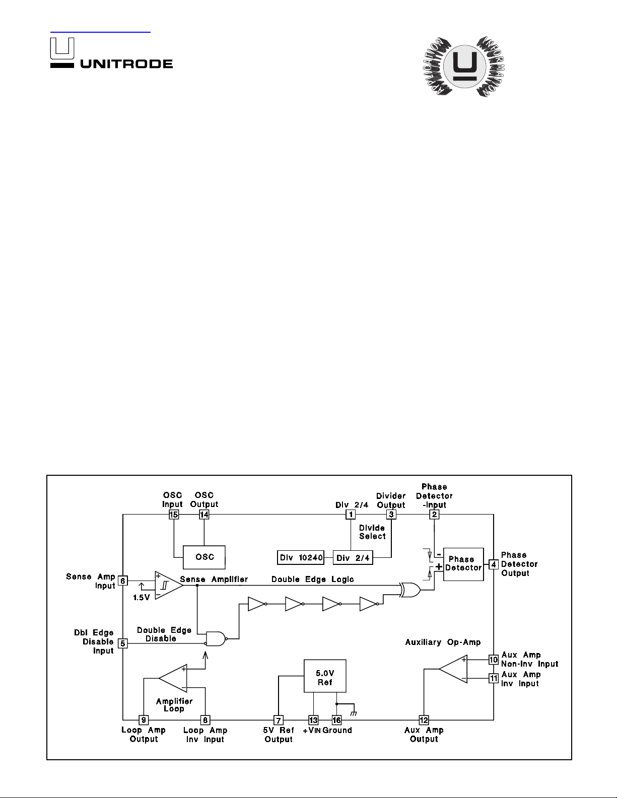
The UC1635 fa mily of i ntegra ted circui ts was desi gned for use in precision speed c ontrol of DC motors. An extension to the UC1633 line of
phase locked controllers, these devices provide access to both of the
digital phase detector ’s inputs, and include a reference frequency divider output pin. With this added flexibility, this family of controllers can
be used to obtain phase synchronization of multiple motors.
A reference frequency can be generated using the device’s crystal oscillator and pro grammabl e divide rs. The osc illator operates using a broad
range of cr ystals, or, can functi on as a buffer stage to an external frequency source.
The phase de tector responds proportional ly to the phase error between
the detector’s minus input pin and the sense amplifier output. This
phase detector includes absolute frequency steering to provide maximum drive sign als when any frequency error exists. This feature allows
optimum start-up and lock times to be realized.
UC1635
UC2635
UC3635
BLOCK DIAGRAM
Two op-amps are included that can be confi gure d to provide necessary
loop filtering. The outputs of these op-amps will source or sink in excess
of 16mA, s o they c an pr ovide a low i mpedan ce cont rol signal to driving
circuits.
Additional features include a double edge option on the sens e amplifier
that can be used to doubl e the loop reference frequency for increased
loop bandwi dths. A 5V reference output can be used to accurately set
DC operating levels.
7/97
UDG-92019
Page 2
UC1635
UC2635
UC3635
ABSOLUTE MAXIMUM RATINGS
Input Supply Voltage (+VIN) . . . . . . . . . . . . . . . . . . . . +20V
Reference Output Current . . . . . . . . . . . . . . . . . . . . . -30mA
Op-Amp Output Currents . . . . . . . . . . . . . . . . . . . . ±30mA
Op-Amp Input Voltages . . . . . . . . . . . . . . . . . . -0.3 to +20V
Phase Detector Input Voltage . . . . . . . . . . . . . -0.3V to +5V
Phase Detector Output Current . . . . . . . . . . . . . . . . ±10mA
Lock Indicator Output Current . . . . . . . . . . . . . . . . . +15mA
Lock Indicator Output Voltage . . . . . . . . . . . . . . . . . . . +20V
Divide Select Input Voltages . . . . . . . . . . . . -0.3V to +10V
Double Edge Disable Input Voltage . . . . . . . -0.3V to +10V
Oscillator Input Voltage . . . . . . . . . . . . . . . . . . -0.3V to +5V
Sense Amplifier Input Voltage . . . . . . . . . . . . -0.3V to +20V
Power Dissipation at TA = 25°C, (Note 2) . . . . . . . 1000mW
Power Dissipation at TC = 25°C, (Note 2) . . . . . . . 2000mW
Operating Junction Temperature . . . . . . . . . -55° to 150°C
Storage Temperature . . . . . . . . . . . . . . . . . -65° to +150°C
Lead Temperature (Soldering, 10 Seconds) . . . . . . . 300°C
Note 1: Vo lt ag es are ref ere nc ed to gro un d, (Pin 16). Currents
are positive into, negative out of, the specified terminals.
Note 2: Consult Uni tro de Int eg rated Circuits databook for in formation regarding therm al specifications and limitations of
packages.
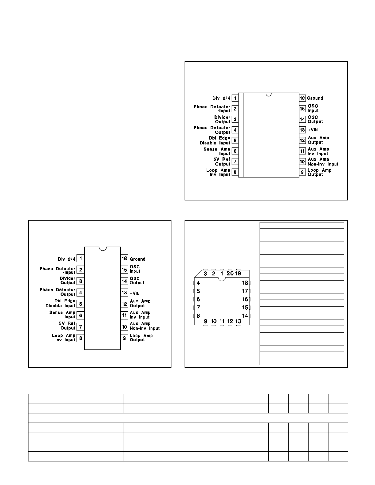
DIL–16 (Top View)
J & N Packages
CONNECTION DIAGRAMS
SOIC–16 (Top View)
DW Package
PLCC-20 & LCC-20
(Top View)
Q & L Packages
N/C 1
Div 2/4 2
Phase Detector Input 3
Divider Output 4
Phase Detector Output 5
N/C 6
Dbl Edge Disable Input 7
Sense Amp Input 8
5V Ref Output 9
Loop Amp Inv Input 10
N/C 11
Loop Amp Output 12
Aux Amp Non-Inv Input 13
Aux Amp Inv Input 14
Aux Amp Output 15
N/C 16
+V
OSC Output 18
OSC Input 19
Ground 20
PACKAGE PIN FUNCTION
FUNCTION
IN
PIN
17
ELECTRICAL
CHARACTERISTICS:
PARAMETER TEST CONDITIONS MIN TYP MAX UNITS
Supply Current +VIN = 15V 20 28 mA
Reference
Output Voltage (V
Load Regulation I
Line Regulation +V
Short Circuit Current V
REF
Unless otherwise stated, specifications hold for T
the UC2635 and -55°C to +125°C for the UC1635, +V
) 4.75 5.0 5.25 V
= 0 to 7mA 5.0 20 mV
OUT
= 8 to 15V 2.0 20 mV
IN
= 0V 15 35 mA
OUT
= 0°C to +70°C for the UC3635, -25°C to +85°C for
A
= 12V. TA = T
IN
J.
2
Page 3

ELECTRICAL CHARACTERISTICS:
-25°C to +85°C for the UC2635 and -55°C to +125°C for the UC1635, +Vin = 12V. T
Unless otherwise stated, spec ifications hold for TA = 0°C to +70°C for the UC3635,
= T
A
J.
PARAMETER TEST CONDITIONS MIN TYP MAX UNITS
Oscillator
DC Voltage Gain Oscillator Input to Oscillator Output 12 16 20 dB
Input DC Level
(VIB)
Input Impedance (Note 2) V
Output DC Level Oscillator Input Pin Open, T
Oscillator Input Pin Open, TJ = 25°C 1.15 1.3 1.45 V
= VIB ±0.5V, TJ = 25°C 1.3 1.6 1.9 kΩ
IN
= 25°C 1.2 1.4 1.6 V
J
Maximum Operating Frequency 10 MHz
Dividers
Maximum Inp ut Frequency Input = 1Vpp at Oscillator Input 10 MHz
Div 2/4 Input Current Input = 5V (Div. by 2) 150 500 µA
Input = 0V (Div. by 4) -5.0 0.0 5.0
Div 2/4 Threshold 0.5 1.6 2.2 V
Divider Output High Level (w/6.8k Load to GND) 4.0 4.5 V
Low Level (Open Collector Leakage) 10 µA
Sense Amplifier
Threshold Voltage Percent of V
REF
27 30 33 %
Threshold Hysteresis 10 mV
Input Bias Current Input = 1.5V -1.0 -0.2 µA
Double Edge Disable Input
Input Current Input = 5V (Disabled) 150 500
Input = 0V (Enabled) -5.0 0.0 5.0 µA
Threshold Voltage 0.5 1.6 2.2 V
Phase Detector
-Input Threshold Detector R esponds to Falling Edge 0.5 1.6 2.2 V
-Input Current Input = 2.2V 100 250
High Output Level Positive Phase/Freq. Error, Volts Below V
REF
0.2 0.5 V
Low Output Level Negative Phase/Freq. Error 0.2 0.5 V
Mid Output Level Zero Phase/Freq. Error, Percent of V
High Level Maximum Source
= 4.3V 2.0 8.0 mA
V
OUT
REF
47 50 53 %
Current
Low Level Maximum Sink Current V
Mid Level Outpu t Im pe da nc e
0.7V 2.0 5.0 mA
OUT
= -200 to +200µA, TJ = 25°C 4.5 6.0 7.5 k
I
OUT
(Note 3)
Loop Amplifier
Non-Inv Reference Voltage Percent of V
REF
47 50 53 %
Input Bias Current Input = 2.5V -0.8 -0.2
AVOL 60 75 dB
PSRR +V
Short Circuit Current Source, V
= 8 to 15V 70 100 dB
IN
= 0V 16 35 mA
OUT
Sink, V
= 5V 16 30 mA
OUT
UC1635
UC2635
UC3635
µ
A
µ
A
µ
A
Ω
µ
A
Note 3: These impedance levels will vary with TJ at about 1700ppm/ °C.
3
Page 4

UC1635
UC2635
UC3635
ELECTRICAL CHARACTERISTICS (cont.):
UC3635, -25°C to +85°C for the UC2635 and -55°C to +125°C for the UC1635, +Vin = 12V. T
Unless otherwise stated, specific at io ns hol d fo r TA = 0°C to +70°C for the
= T
A
J.
PARAMETER TEST CONDITIONS MIN TYP MAX UNITS
Auxiliary Op-Amp
Input Offset Voltage V
Input Bias Current V
Input Offset Current V
= 2.5V 8 mV
CM
= 2.5V -0.8 -0.2 µA
CM
= 2.5V .01 0.1 µA
CM
AVOL 70 120 dB
PSRR +V
CMRR V
Short Circuit Current Source, V
= 8 to 15V 70 100 dB
IN
= 0 to 10V 70 100 dB
CM
= 0V 16 35 mA
OUT
Sink, V
= 5V 16 30 mA
OUT
Application and Operation Information
(For Additional Application Information see the UC1633 Data Sheet)
(Pin numbers refer to DIL and SOIC packages)
Phase Detector Input Detail
Reference Divider Output Detail
UNITRODE CORPORATI ON
7 CONTINENTAL BLVD. • MERRIMACK, NH 03054
TEL. (603) 424- 24 10 • FAX (603) 424-3460
UDG-92012
UDG-92011-1
4
Page 5

IMPORTANT NOTICE
T exas Instruments and its subsidiaries (TI) reserve the right to make changes to their products or to discontinue
any product or service without notice, and advise customers to obtain the latest version of relevant information
to verify, before placing orders, that information being relied on is current and complete. All products are sold
subject to the terms and conditions of sale supplied at the time of order acknowledgement, including those
pertaining to warranty, patent infringement, and limitation of liability.
TI warrants performance of its semiconductor products to the specifications applicable at the time of sale in
accordance with TI’s standard warranty. Testing and other quality control techniques are utilized to the extent
TI deems necessary to support this warranty . Specific testing of all parameters of each device is not necessarily
performed, except those mandated by government requirements.
CERTAIN APPLICA TIONS USING SEMICONDUCT OR PRODUCTS MAY INVOLVE POTENTIAL RISKS OF
DEATH, PERSONAL INJURY, OR SEVERE PROPERTY OR ENVIRONMENTAL DAMAGE (“CRITICAL
APPLICATIONS”). TI SEMICONDUCTOR PRODUCTS ARE NOT DESIGNED, AUTHORIZED, OR
WARRANTED TO BE SUITABLE FOR USE IN LIFE-SUPPORT DEVICES OR SYSTEMS OR OTHER
CRITICAL APPLICA TIONS. INCLUSION OF TI PRODUCTS IN SUCH APPLICATIONS IS UNDERST OOD TO
BE FULLY AT THE CUSTOMER’S RISK.
In order to minimize risks associated with the customer’s applications, adequate design and operating
safeguards must be provided by the customer to minimize inherent or procedural hazards.
TI assumes no liability for applications assistance or customer product design. TI does not warrant or represent
that any license, either express or implied, is granted under any patent right, copyright, mask work right, or other
intellectual property right of TI covering or relating to any combination, machine, or process in which such
semiconductor products or services might be or are used. TI’s publication of information regarding any third
party’s products or services does not constitute TI’s approval, warranty or endorsement thereof.
Copyright 1999, Texas Instruments Incorporated
 Loading...