

Page 1
Philips Semiconductors Linear Products Product specification
µA747CDual operational amplifier
54
August 31, 1994 853-0899 13721
DESCRIPTION
The 747 is a pair of high-performance monolithic operational
amplifiers constructed on a single silicon chip. High common-mode
voltage range and absence of “latch-up” make the 747 ideal for use
as a voltage-follower. The high gain and wide range of operating
voltage provides superior performance in integrator, summing
amplifier, and general feedback applications. The 747 is short-circuit
protected and requires no external components for frequency
compensation. The internal 6dB/octave roll-off insures stability in
closed-loop applications. For single amplifier performance, see
µA741 data sheet.
FEATURES
•No frequency compensation required
•Short-circuit protection
•Offset voltage null capability
•Large common-mode and differential voltage ranges
•Low power consumption
•No latch-up
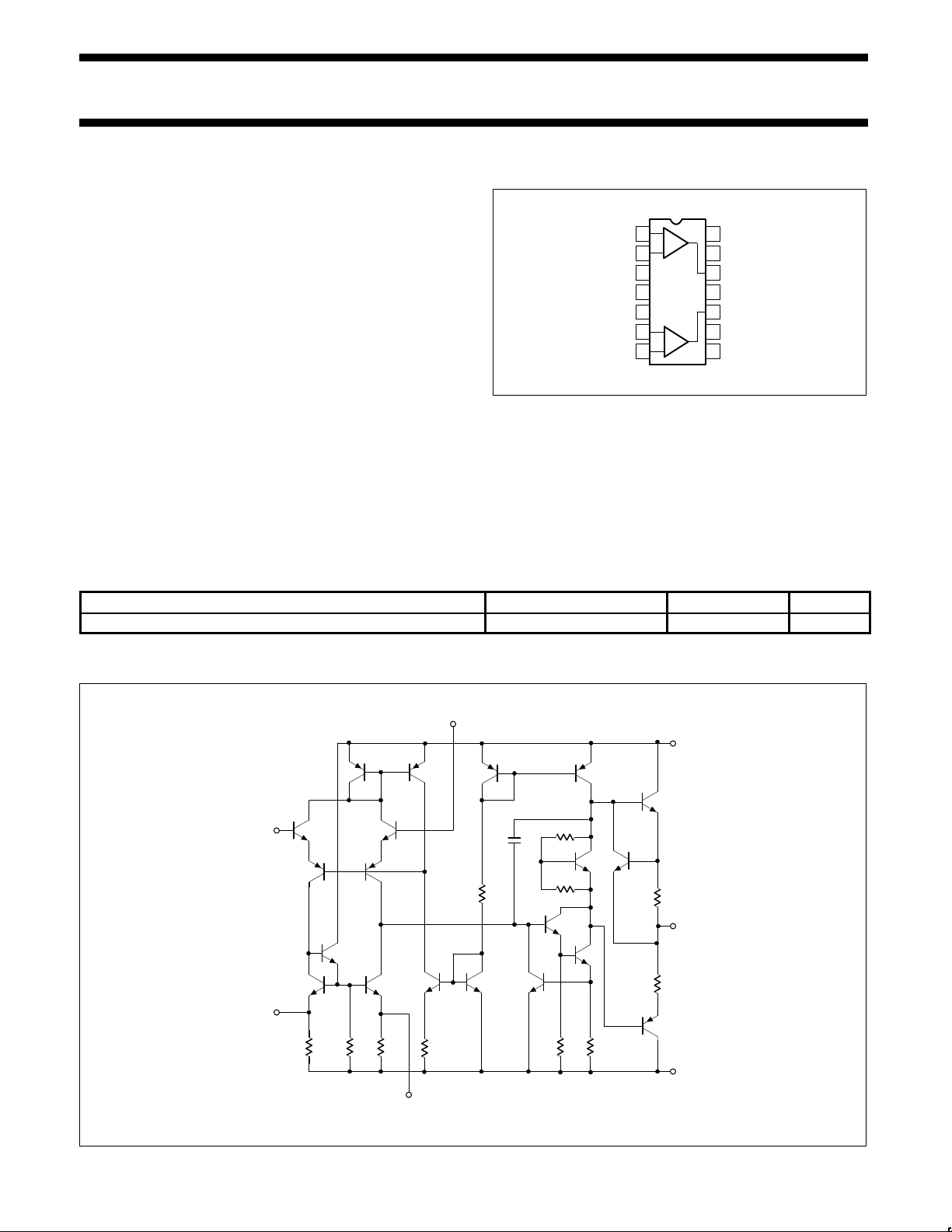
PIN CONFIGURATION
+
B
A
–
INVERTING INPUT B
NON–INVERTING INPUT B
OFFSET NULL B
V–
OFFSET NULL A
NON–INVERTING INPUT A
INV. INPUT A
OFFSET NULL B
V + B
OUTPUT B
1
2
3
4
5
6
7 8
14
13
12
11
10
9
OFFSET NULL A
V + A
OUTPUT A
NO CONNECT
N Package
TOP VIEW
–
+
ORDERING INFORMATION
DESCRIPTION TEMPERATURE RANGE ORDER CODE DWG #
14-Pin Plastic DIP 0°C to 70°C µA747CN 0405B
EQUIVALENT SCHEMATIC
NON–INVERTING
INPUT
Q1
Q8
Q2
Q3
Q4
Q7
Q5
Q6
R1
1KΩR350KΩ
R2
1KΩ
Q9
Q13
R5
39KΩ
Q10 Q11 Q22
V+
Q14
R9
25Ω
OUTPUT
R10
50Ω
Q20
Q16
Q17
Q18 Q15
V–
R11
50Ω
R12
50kΩ
R7
4.5Ω
R8
7.5KΩ
R4
5kΩ
30pF
Q12
OFFSET NULL
INVERTING INPUT
OFFSET NULL
Page 2
Philips Semiconductors Linear Products Product specification
µA747CDual operational amplifier
August 31, 1994
55
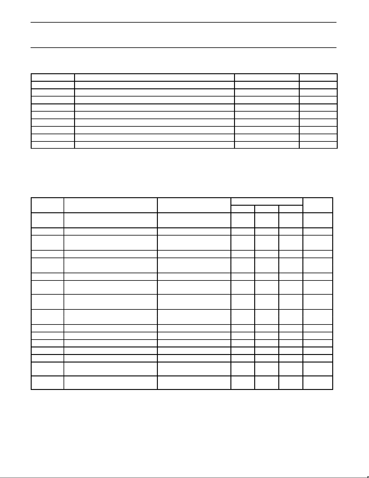
ABSOLUTE MAXIMUM RATINGS
SYMBOL PARAMETER RATING UNIT
V
S
Supply voltage ±18 V
P
D MAX
Maximum power dissipation TA=25°C (still air)
1
1500 mW
V
IN
Differential input voltage ±30 V
V
IN
Input voltage
2
±15 V
Voltage between offset null and V- ±0.5 V
T
STG
Storage temperature range -65 to +150 °C
T
A
Operating temperature range 0 to +70 °C
T
SOLD
Lead temperature (soldering, 10sec) 300 °C
I
SC
Output short-circuit duration Indefinite
NOTES:
1. Derate above 25°C at the following rates:
N package at 12mW/°C
2. For supply voltages less than ±15V, the absolute maximum input voltage is equal to the supply voltage.
DC ELECTRICAL CHARACTERISTICS
TA=25°C, V
CC
= ±15V unless otherwise specified.
µA747C
SYMBOL
PARAMETER
TEST CONDITIONS
Min Typ Max
UNIT
V
OS
Offset voltage RS≤10kΩ 2.0 6.0 mV
RS≤10kΩ, over temp. 3.0 7.5 mV
∆VOS/∆T 10 µV/°C
I
OS
Offset current 20 200 nA
Over temperature 7.0 300 nA
∆IOS/∆T 200 pA/°C
I
BIAS
Input current 80 500 nA
Over temperature 30 800 nA
∆IB/∆T 1 nA/°C
V
OUT
Output voltage swing
RL≥2kΩ, over temp.
R
L
≥10kΩ, over temp.
±10
±12
±13
±14
V
V
I
CC
Supply current each side 1.7 2.8 mA
Over temperature 2.0 3.3 mA
P
d
Power consumption 50 85 mW
Over temperature 60 100 mW
C
IN
Input capacitance 1.4 pF
Offset voltage adjustment range ±15 mV
R
OUT
Output resistance 75 Ω
Channel separation 120 dB
PSRR Supply voltage rejection ratio RS≤10kΩ, over temp. 30 150 µV/V
A
VOL
Large-signal voltage gain (DC)
RL≥2kΩ, V
OUT
=±10V
Over temperature
25,000
15,000
V/V
V/V
CMRR Common-mode rejection ratio
RS≤10kΩ, VCM=±12V
Over temperature
70 dB
Page 3
Philips Semiconductors Linear Products Product specification
µA747CDual operational amplifier
August 31, 1994
56
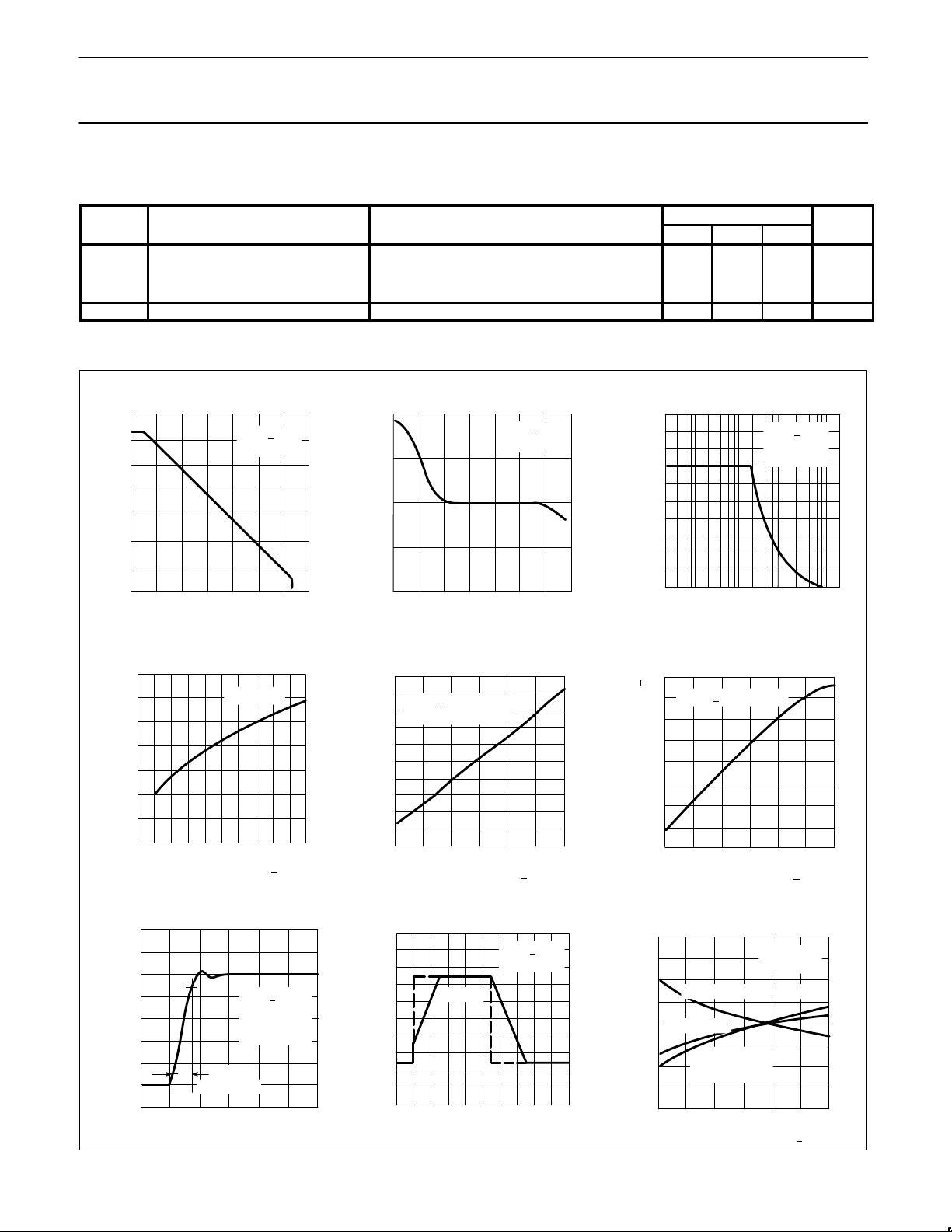
AC ELECTRICAL CHARACTERISTICS
TA=25°C, V
S
= ±15V unless otherwise specified.
µA747C
SYMBOL
PARAMETER
TEST CONDITIONS
Min Typ Max
UNIT
Transient response VIN=20mV, RL=2kΩ, CL<100pF
t
R
Rise time Unity gain CL≤100pF 0.3 µs
Overshoot Unity gain CL≤100pF 5.0 %
SR Slew rate RL>2kΩ 0.5 V/µs
TYPICAL PERFORMANCE CHARACTERISTICS
COMMON MODE VOLTAGE RANGE — V
+
–55oC < TA < +125oC
16
14
12
10
8
6
4
2
0
5 10 15 20
SUPPLY VOLTAGE — +
V
Frequency Characteristics as a
Function of Supply Voltage
VOLTAGE GAIN
VS = + 15V
T
A
= 25oC
10
6
10
5
10
4
10
3
10
2
10
1
1 10 100 1K 10K 100K 1M 10M
FREQUENCY — Hz
Open–Looped Voltage Gain
as a Function of Frequency
PHASE DEGREES
1 10 100 1K 10K 100K 1M 10M
VS = + 15V
T
A
= 25oC
0
–45
–90
–135
–180
FREQUENCY — Hz
Open–Looped Voltage Response
as a Function of Frequency
PEAK–TO–PEAK OUTPUT SWING — V
40
36
32
28
24
20
16
12
8
4
0
100 1k 10k 100k 1M
FREQUENCY — Hz
VS = + 15V
T
A
= 25oC
R
L
= 10kΩ
Output Voltage Swing
as a Function of Frequency
115
110
105
100
95
90
85
80
0 4 8 12 15 20
SUPPLY VOLTAGE — +
V
VOLTAGE GAIN — dB
TA = 25OC
Open–Loop Voltage Gain as a
Function of Supply Voltage
PEAK TO PEAK OUTPUT SWING — V
–55oC < TA < +125oC
R
L
> 2kΩ
40
36
32
28
24
20
16
12
8
4
0
5 10 15 20
SUPPLY VOLTAGE — +
V
Output Voltage Swing as a
Function of Supply Voltage
OUTPUT — mV
28
24
20
16
12
8
4
0
0 0.5 1.0 1.5 2.0 2.5
TIME — µs
VS = + 15V
T
A
= 25oC
R
L
= 2kΩ
C
L
= 100pF
10%
RISE TIME
Transient Response
10
8
6
4
2
0
–2
–4
–6
–8
–10
0 10 20 30 40 50 60 70 80 90
TIME — µS
OUTPUT
INPUT
VS = + 15V
T
A
= 25oC
OUTPUT VOLTAGE — V
Voltage-follower Large-Signal
Pulse Response
1.4
1.2
1.0
0.8
0.6
5 10 15 20
SUPPLY VOLTAGE — +
V
RELATIVE VALUE
TRANSIENT RESPONSE
SLEW RATE
CLOSED
LOOP
BANDWIDTH
T
A
= 25
o
C
Input Common–Mode Voltage Range
as a Function of Supply voltage
–1
Page 4
Philips Semiconductors Linear Products Product specification
µA747CDual operational amplifier
August 31, 1994
57
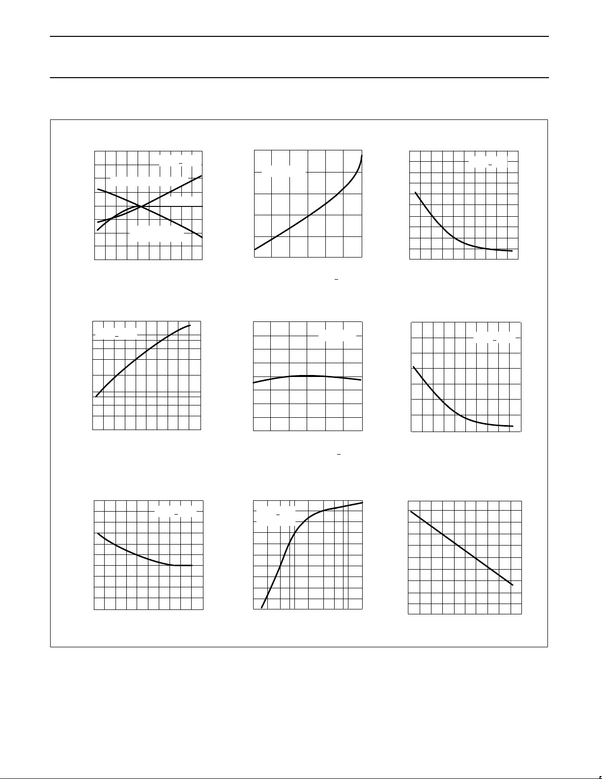
TYPICAL PERFORMANCE CHARACTERISTICS (Continued)
Power Consumption as a Function
of Ambient Temperature
Output Short–Circuit Current
as a Function of
Ambient Temperature
RELATIVE VALUE
Frequency Characteristics as a
Function of Ambient Temperature
1.4
1.2
1.0
0.8
0.6
TRANSIENT RESPONSE
–60 –20 20 80 100 140
TEMPERATURE —
o
C
VS = + 15V
CLOSED LOOP
BANDWIDTH
SLEW RATE
POWER CONSUMPTION — mW
TA = 25oC
100
80
60
40
20
0
5 10 15 20
TA = 25oC
SUPPLY VOLTAGE — +
V
Power Consumption as a
Function of Supply Voltage
INPUT BIAS CURRENT — nA
VS = +15V
500
400
300
200
100
0
–60 –20 20 60 100 140
TEMPERATURE —
o
C
Input Bias Current as a Function
of Ambient Temperature
INPUT RESISTANCE — MΩ
10.0
5.0
3.0
1.0
0.5
0.3
0.1
–60 –20 20 60 100 140
TEMPERATURE —
o
C
Input Resistance as a Function
of Ambient Temperature
VS = + 15V
40
30
20
10
0
5 10 15 20
SUPPLY VOLTAGE —
+V
INPUT OFFSET CURRENT — nA
TA = 25oC
Input Offset Current as a
Function of Supply Voltage
140
120
100
80
60
40
20
0
–60 –20 20 60 100 140
TEMPERATURE
—
o
C
INPUT OFFSET CURRENT — nA
VS = + 15V
Input Offset Current as a Function
of Ambient Temperature
70
60
50
40
30
–60 –20 20 60 100 140
TEMPERATURE
—
o
C
POWER CONSUMPTION — mW
VS = + 15V
PEAK–TO–PEAK OUTPUT SWING — V
VS = +15V
T
A
= 25oC
28
26
24
22
20
18
16
14
12
10
8
0.1 0.2 0.5 1.0 2.0 5.0 10
LOAD RESISTANCE — kΩ
Output Voltage Swing as a
Function of Load Resistance
SHORT CIRCUIT CURRENT — mA
35
30
25
20
15
10
–60 –20 20 60 100 140
TEMPERATURE —
o
C
Page 5
Philips Semiconductors Linear Products Product specification
µA747CDual operational amplifier
August 31, 1994
58
TYPICAL PERFORMANCE CHARACTERISTICS (Continued)
MEAN SQUARE VOLTAGE — V Hz
2
10
–13
10
–14
10
–15
10
–16
10
–17
10
–18
10 100 1K 10K 100K
FREQUENCY — Hz
VS = + 15V
T
A
= 25oC
MEAN SQUARE VOLTAGE — V Hz
2
MEAN SQUARE NOISE CURRENT
10
–21
10
–22
10
–23
10
–24
10
–25
10
–26
10 100 1K 10K 100K
FREQUENCY — Hz
Broadband Noise for
Various Bandwidths
TOTAL NOISE REFERRED TO INPUT — Vrmsµ
10–1kHz
100
10
1
0.1
100 1K 10K 100K
10–100kHz
10–10kHz
SOURCE RESISTANCE — Ω
VS = + 15V
T
A
= 25oC
Input Noise Current
as a Function of Frequency
Input Noise Voltage
as a Function of Frequency
VS = + 15V
T
A
= 25oC
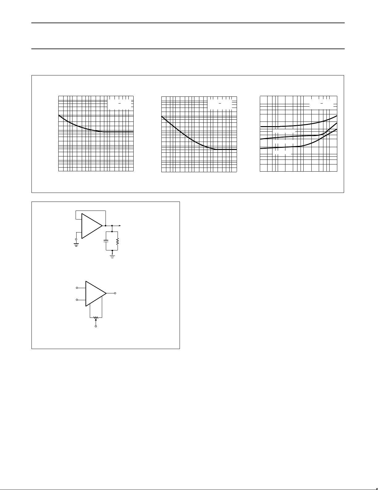
TEST CIRCUITS
+
–
µA747C
V
IN
C
L
R
L
V
OUT
10KΩ
–V
+
–
µA747C
Transient Response Test Circuit
Voltage Offset Null Circuit
 Loading...