

Datasheet U631H64BSC45, U631H64BSC35, U631H64BSC25, U631H64SC25, U631H64BDK45 Datasheet (ZMD)
...Page 1
Features
p
High-performance CMOS nonvolatile static RAM 8192 x 8 bits
p
25, 35 and 45 ns Access Times
p
12, 20 and 25 ns Output Enable
Access Times
p
Software STORE Initiation
(STORE Cycle Time < 10 ms)
p
Automatic STORE Timing
p
105 STORE cycles to EEPROM
p
10 years data retention in
EEPROM
p
Automatic RECALL on Power Up
p
Software RECALL Initiation
(RECALL Cycle Time < 20 µs)
p
Unlimited RECALL cycles from
EEPROM
p
Unlimited Read and Write to
SRAM
p
Single 5 V ± 10 % Operation
p
Operating temperature ranges:
p
CECC 90000 Quality Standard
p
ESD characterization according
MIL STD 883C M3015.7-HBM
(classification see IC Code
Numbers)
0 to 70 °C
-40 to 85 °C
p
Packages:PDIP28 (300 mil)
SOP28 (330 mil)
Description
The U631H64 has two separate
modes of operation: SRAM mode
and nonvolatile mode. In SRAM
mode, the memory operates as an
ordinary static RAM. In nonvolatile
operation, data is transferred in
parallel from SRAM to EEPROM or
from EEPROM to SRAM. In this
mode SRAM functions are disabled.
The U631H64 is a fast static RAM
(25, 35, 45 ns), with a nonvolatile
electrically erasable PROM
(EEPROM) element incorporated
in each static memory cell. The
SRAM can be read and written an
unlimited number of times, while
independent nonvolatile data resides in EEPROM. Data transfers
from the SRAM to the EEPROM
(the STORE operation), or from the
EEPROM to the SRAM (the
RECALL operation) are initiated
through software sequences.
U631H64
SoftStore
The U631H64 combines the high
performance and ease of use of a
fast SRAM with nonvolatile data
integrity.
Once a STORE cycle is initiated,
further input or output are disabled
until the cycle is completed.
Because a sequence of addresses
is used for STORE initiation, it is
important that no other read or write
accesses intervene in the sequence
or the sequence will be aborted.
Internally, RECALL is a two step
procedure. First, the SRAM data is
cleared and second, the nonvolatile
information is transferred into the
SRAM cells.
The RECALL operation in no way
alters the data in the EEPROM
cells. The nonvolatile data can be
recalled an unlimited number of
times.
8K x 8 nvSRAM
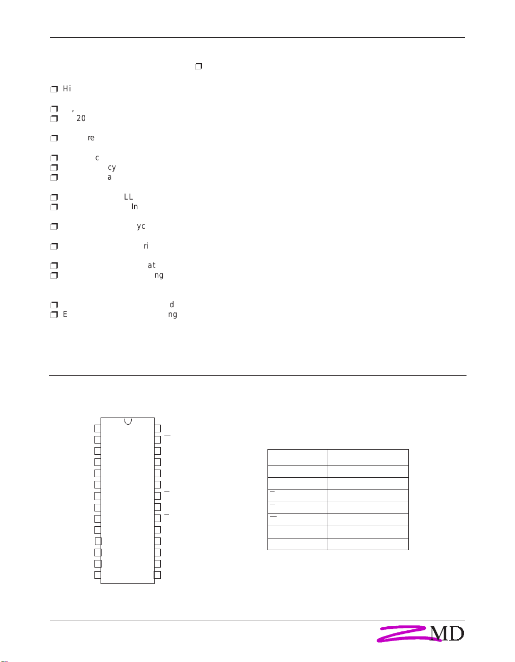
Pin Configuration Pin Description
PDIP
SOP
28
VCC
27
W
26
n.c.
25
A8
24
A9
23
A11
22
G
21
A10
20
E
19
DQ7
18
DQ6
17
DQ5
16
DQ4
15
DQ3
Signal Name Signal Description
A0 - A12 Address Inputs
DQ0 - DQ7 Data In/Out
E
G
W
VCC Power Supply Voltage
VSS Ground
1
1
n.c.
2
A12
3
A7
4
A6
5
A5
6
A4
7
A3
8
A2
9
A1
10
A0
11
DQ0
12
DQ1
13
DQ2
14
VSS
Top View
December 12, 1997
Chip Enable
Output Enable
Write Enable
Page 2
U631H64
Block Diagram
A5
A6
A7
A8
A9
A11
A12
DQ0
DQ1
DQ2
DQ3
DQ4
DQ5
DQ6
DQ7
64 x 8 Columns
Row Decoder
Column Decoder
Input Buffers
A0 A1 A2 A3 A4A10
EEPROM Array
Array
128 Rows x
Column I/O
128 x (64 x 8)
STORE
RECALLSRAM
Store/
Recall
Control
Software
Detect
Truth Table for SRAM Operations
Operating Mode E W G DQ0 - DQ7
Standby/not selected H
**
Internal Read L H H High-Z
Read L H L Data Outputs Low-Z
Write L L
*
Data Inputs High-Z
*H or L
V
V
V
G
E
W
High-Z
CC
SS
CC
A0 - A12
Characteristics
All voltages are referenced to VSS = 0 V (ground).
All characteristics are valid in the power supply voltage range and in the operating temperature range specified.
Dynamic measurements are based on a rise and fall time of ≤ 5 ns, measured between 10 % and 90 % of V
input levels of V
with the exception of the t
Absolute Maximum Rating
Power Supply Voltage V
Input Voltage V
Output Voltage V
Power Dissipation P
Operating Temperature C-Type
Storage Temperature T
a:Stresses greater than those listed under „Absolute Maximum Ratings“ may cause permanent damage to the device. This is a stress
rating only, and functional operation of the device at condition above those indicated in the operational sections of this specification is
not implied. Exposure to absolute maximum rating conditions for extended periods may affect reliability.
= 0 V and VIH = 3 V. The timing reference level of all input and output signals is 1.5 V,
IL
-times and ten-times, in which cases transition is measured ± 200 mV from steady-state voltage.
dis
a
K-Type
Symbol Min. Max. Unit
CC
I
O
D
T
a
stg
-0.5 7 V
-0.3 VCC+0.5 V
-0.3 VCC+0.5 V
0
-40
-65 150 °C
2
,as well as
I
1W
70
85
°C
°C
December 12, 1997
Page 3
U631H64
Recommended Operation
Conditions
Power Supply Voltage V
Input Low Voltage V
Input High Voltage V
Symbol Conditions Min. Max. Unit
CC
-2 V at Pulse Width
IL
10 ns permitted
IH
DC Characteristics Symbol Conditions
Operating Supply Current
Average Supply Current during
c
STORE
Standby Supply Current
(Cycling TTL Input Levels)
b
d
I
V
CC1
V
V
t
t
t
V
I
CC2
E
W
V
V
I
CC(SB)1VCC
E
= 5.5 V
CC
= 0.8 V
IL
= 2.2 V
IH
= 25 ns
c
= 35 ns
c
= 45 ns
c
= 5.5 V
CC
≥ V
-0.2 V
CC
≥ V
-0.2 V
CC
≤ 0.2 V
IL
≥ V
IH
CC
-0.2 V
= 5.5 V
≥ V
IH
4.5 5.5 V
-0.3 0.8 V
2.2 VCC+0.3 V
C-Type K-Type
Min. Max. Min. Max.
90
80
75
95
85
80
67mA
Unit
mA
mA
mA
t
= 25 ns
c
= 35 ns
t
c
= 45 ns
t
c
Average Supply Current
at t
= 200 ns
cR
(Cycling CMOS Input Levels)
Standby Supply Current
(Stable CMOS Input Levels)
b:I
and I
CC1
The current I
c:I
is the average current requird for the duration of the STORE cycle (STORE Cycle Time).
CC2
d: Bringing E
table. The current I
b
d
are dependent on output loading and cycle rate. The specified values are obtained with outputs unloaded.
CC3
is measured for WRITE/READ - ratio of 1/2.
CC1
≥ VIH will not produce standby current levels until any nonvolatile cycle in progress has timed out. See MODE SELECTION
is measured for WRITE/READ - ratio of 1/2.
CC(SB)1
I
CC(SB)
December 12, 1997
I
CC3
V
= 5.5 V
CC
≥ V
W
≤ 0.2 V
V
IL
≥ V
V
IH
V
= 5.5 V
CC
≥ V
E
≤ 0.2 V
V
IL
≥ V
V
IH
3
CC
CC
CC
CC
-0.2 V
-0.2 V
-0.2 V
-0.2 V
30
23
20
34
27
23
mA
mA
mA
15 15 mA
11mA
Page 4
U631H64
DC Characteristics Symbol Conditions
Output High Voltage
Output Low Voltage
Output High Current
Output Low Current
Input Leakage Current
Output Leakage Current
High at Three-State- Output
Low at Three-State- Output
High
Low
V
V
I
I
OH
OL
I
OH
I
OL
I
IH
I
IL
OHZ
OLZ
V
CC
I
OH
I
OL
V
CC
V
OH
V
OL
V
CC
V
IH
V
IL
V
CC
V
OH
V
OL
= 4.5 V
=-4 mA
= 8 mA
= 4.5 V
= 2.4 V
= 0.4 V 8
= 5.5 V
= 5.5 V
= 0 V -1
= 5.5 V
= 5.5 V
= 0 V -1
SRAM MEMORY OPERATIONS
Switching Characteristics
No.
Read Cycle
1 Read Cycle Time
2 Address Access Time to Data Valid
f
g
3 Chip Enable Access Time to Data Valid t
4 Output Enable Access Time to Data Valid t
5E
HIGH to Output in High-Z
6G
HIGH to Output in High-Z
h
h
7E LOW to Output in Low-Z t
8G
LOW to Output in Low-Z t
9 Output Hold Time after Addr. Change
g
10Chip Enable to Power Activee t
11Chip Disable to Power Standby
d, e
Symbol 25 35 45
Alt.IECMin.Max.Min.Max.Min.Max.
t
AVAVtcR
t
AVQVta(A)
ELQVta(E)
GLQVta(G)
t
EHQZtdis(E)
t
GHQZtdis(G)
ELQXten(E)
GLQXten(G)
t
AXQXtv(A)
t
ELICCH
t
EHICCL
PU
t
PD
C-Type K-Type
Unit
Min. Max. Min. Max.
2.4
0.4
-4
1
1
2.4
-1
-1
8
0.4VV
-4 mA
mA
1 µA
µA
1 µA
µA
Unit
25 35 45 ns
25 35 45 ns
25 35 45 ns
12 20 25 ns
13 17 20 ns
13 17 20 ns
555ns
000ns
333ns
000ns
25 35 45 ns
e: Parameter guaranteed but not tested.
f: Device is continuously selected with E
g:Address valid prior to or at the same time with E
h:Measured ± 200 mV from steady state output voltage.
and G both LOW.
transition LOW.
4
December 12, 1997
Page 5

U631H64
AAAA
AAAA
AAAA
AAAA
AAAA
AAAA
AAAA
AAAA
AAAA
AAAA
AAAA
AAAA
Read Cycle 1: Ai-controlled (during Read cycle: E = G = VIL, W = VIH)
1
t
Ai
DQi
Output
Previous
Data Valid
9
t
v(A)
Read Cycle 2: G-, E-controlled (during Read cycle: W = VIH)
t
t
en(E)
t
en(G)
10
t
PU
Address Valid
2
a(A)
7
8
Ai
E
G
DQi
Output
I
CC
High Impedance
ACTIVE
STANDBY
Address Valid
2
t
a(A)
1
t
cR
3
t
a(E)
4
t
a(G)
cR
g
Output Data
Valid
f
Output Data
Valid
5
t
dis(E)
6
t
dis(G)
11
t
PD
Switching Characteristics
No.
Write Cycle
12Write Cycle Time t
13Write Pulse Width t
14Write Pulse Width Setup Time t
15Address Setup Time t
16Address Valid to End of Write t
17Chip Enable Setup Time t
18Chip Enable to End of Write t
19Data Setup Time to End of Write t
20Data Hold Time after End of Write t
21Address Hold after End of Write t
22W
LOW to Output in High-Z
23W
HIGH to Output in Low-Z t
h, i
December 12, 1997
Symbol 25 35 45
Alt. #1Alt. #2 IEC Min. Max. Min. Max. Min. Max.
t
AVAVtAVAV
WLWH
WLEHtsu(W)
AVWLtAVELtsu(A)
AVWHtAVEH
ELWH
ELEHtw(E)
DVWHtDVEHtsu(D)
WHDXtEHDXth(D)
WHAXtEHAXth(A)
t
WLQZ
WHQX
t
w(W)
t
su(A-WH)
t
su(E)
t
dis(W)
t
en(W)
25 35 45 ns
cW
20 30 35 ns
20 30 35 ns
000ns
20 30 35 ns
20 30 35 ns
20 30 35 ns
12 18 20 ns
000ns
000ns
10 13 15 ns
555ns
5
Unit
Page 6

U631H64
A
A
A
AAAA
AAAA
A
A
A
AAAA
AAAA
AAAA
A
A
A
A
AAAA
AAAA
A
A
A
A
AAAA
AAAA
AAAA
AAAA
AAAA
AAAA
AAAA
AAAA
AAAA
AAAA
AAAA
AAAA
AAAA
AAAA
AAAA
AAAA
AAAA
AAAA
AAAA
AAAA
AAAA
AAAA
AAAA
AAAA
AAA
AAA
AAA
AAA
AAA
AAA
AAAA
AAAA
AAAA
AAAA
AAAA
AAAA
A
A
A
AAAA
AAAA
AAAA
AAAA
AAAA
AAAA
AAA
AAA
AAA
AAAA
AAAA
AAAA
AAAA
AAAA
AAAA
AAAA
AAAA
AAAA
AAAA
AAAA
AAAA
AAAA
AAAA
AAAA
AAAA
AAAA
AAAA
AAAA
AAAA
AAAA
AAA
AAA
AAA
Write Cycle #1: W-controlled
Ai
E
W
DQi
Input
DQi
Output
Write Cycle #2: E-controlled
Ai
E
W
DQi
Input
DQi
Output
j
15
t
su(A)
Previous Data
j
15
t
su(A)
12
t
cW
Address Valid
17
t
su(E)
16
t
su(A-WH)
13
t
w(W)
19 20
t
su(D)
Input Data
Valid
22
t
dis(W)
High Impedance
12
t
cW
Address Valid
18 21
t
w(E)
14
t
su(W)
19
t
su(D)
Input Data
Valid
High Impedance
t
t
h(D)
23
en(W)
t
h(A)
21
t
h(A)
20
t
h(D)
AAA
AAAA
AAA
AAA
AAAA
undefined
i: If W is LOW and when E goes LOW, the outputs remain in the high impedance state.
j: E
or W must be
>
during address transitions.
V
IH
AAA
AAAA
AAA
AAA
L- to H-level
AAA
AAA
AAA
AAAA
AAAA
AAAA
6
AAAA
AAAA
AAAA
H- to L-level
AAA
AAA
AAA
AAAA
AAAA
AAAA
AAAA
AAAA
AAAA
December 12, 1997
Page 7

NONVOLATILE MEMORY OPERATIONS
AAAA
AAAA
AAAA
AAAA
AAAA
AAAA
AAAA
AAAA
AAAA
AAAA
AAAA
A
U631H64
STORE CYCLE INHIBIT and
No.
AUTOMATIC POWER UP RECALL
24Power Up RECALL Duration
k, e
Low Voltage Trigger Level V
k:t
starts from the time VCC rises above V
RESTORE
SWITCH
.
Symbol
Alt. IEC
t
RESTORE
SWITCH
STORE CYCLE INH IBIT and AUTOMATIC POWER UP RECALL
V
CC
5.0 V
V
SWITCH
Power Up
RECALL
24
t
RESTORE
Min. Max. Unit
650 µs
4.0 4.5 V
t
STORE inhibit
SOFTWARE MODE SELECTION
E
W
A12 - A0
(hex)
LH0000
1555
0AAA
1FFF
10F0
0F0F
LH0000
1555
0AAA
1FFF
10F0
0F0E
l: The six consecutive addresses must be in order listed (0000, 1555, 0AAA, 1FFF, 10F0, 0F0F) for a Store cycle or (0000, 1555, 0AAA,
1FFF, 10F0, 0F0E) for a RECALL cycle. W
diagrams for further details.
The following six-address sequence is used for testing purposes and should not be used: 0000, 1555, 0AAA, 1FFF, 10F0, 139C.
m: I/O state assumes that G
≤ VIL. Activation of nonvolatile cycles does not depend on the state of G .
must be high during all six consecutive cycles. See STORE cycle and RECALL cycle tables and
December 12, 1997
Mode I/O Power Notes
Read SRAM
Read SRAM
Read SRAM
Read SRAM
Read SRAM
Nonvolatile STORE
Read SRAM
Read SRAM
Read SRAM
Read SRAM
Read SRAM
Nonvolatile RECALL
Output Data
Output Data
Output Data
Output Data
Output Data
Output High Z
Output Data
Output Data
Output Data
Output Data
Output Data
Output High Z
Active
I
CC2
Active l, m
7
l, m
l, m
l, m
l, m
l, m
l
l, m
l, m
l, m
l, m
l
Page 8

U631H64
AAAA
AAAA
AAAA
AAAA
AAAA
AAAA
AAAA
AAAA
AAAA
AAAA
AAAA
AAAA
AAAA
AAAA
AAAA
A
A
A
AAAA
AAAA
AAAA
AAAA
AAAA
AAAA
AAAA
AAAA
AAAA
AAAA
AAAA
AAAA
AAAA
AAAA
AAAA
AAAA
AAAA
AAAA
AAAA
AAAA
AAAA
AAAA
AAAA
AAAA
AAAA
AAAA
AAAA
AAAA
AAAA
AAAA
AAAA
AAAA
AAAA
AAAA
AAAA
AAAA
AAAA
AAAA
AAAA
AAAA
AAAA
AAAA
AAAA
AAAA
AAAA
AAAA
AAAA
AAAA
AAAA
AAAA
AAAA
AAAA
AAAA
AAAA
AAAA
AAAA
AAAA
AAAA
A
A
A
A
AAAA
AAAA
AAAA
AAA
AAA
AAA
AAAA
AAAA
AAAA
AAAA
A
A
A
A
AAAA
AAAA
AAAA
AAAA
AAAA
AAAA
AAAA
AAAA
AAAA
AAAA
AAAA
AAAA
A
A
A
AAAA
AAAA
AAAA
AA
AA
AA
No.Software Controlled STORE/RECALL
25STORE/RECALL Initiation Time t
26Chip Enable to Output Inactive
27STORE Cycle Time
28RECALL Cycle Time
29Address Setup to Chip Enable
30Chip Enable Pulse Width
31Chip Disable to Address Change
n:The software sequence is clocked with E controlled READs.
o:Once the software controlled STORE or RECALL cycle is initiated, it completes automatically, ignoring all inputs.
p:Note that STORE cycles (but not RECALL) are aborted by V
q: An automatic RECALL also takes place at power up, starting when V
V
r: Noise on the E
s: If the Chip Enable Pulse Width is less than t
the end of the low pulse, however the STORE or RECALL will still be initiated.
SOFTWARE CONTROLLED STORE/RECALL CYCLE
l, n
Cycle
o
p
q
r
r, s
r
once it has been exceeded for the RECALL to function properly.
SWITCH
pin may trigger multiple READ cycles from the same address and abort the address sequence.
(see Read Cycle) but greater than or equal t
a(E)
25
t
cR
Ai
ADDRESS 1
Alt. IEC Min. Max. Min. Max. Min. Max.
< V
t
cR
(STORE inhibit).
SWITCH
exceeds V
CC
r, s, t, u
(E = HIGH after STORE initiation)
AVAV
t
ELQZtdis(E)SR
t
ELQXStd(E)S
t
ELQXRtd(E)R
t
AVELNtsu(A)SR
t
ELEHNtw(E)SR
t
EHAXNth(A)SR
CC
Symbol
25 35 45
25 35 45 ns
600 600 600 ns
10 10 10 ms
20 20 20 µs
000ns
20 25 35 ns
000ns
SWITCH
25
t
cR
ADDRESS 6
and takes t
, than the data may not be valid at
w(E)SR
. VCC must not drop below
RESTORE
31
t
E
High Impedance
DQi
Output
SOFTWARE CONTROLLED STORE/RECALL CYCLE
Ai
t
w(E)SR
29
t
su(A)SR
t
h(A)SR
31
VALID VALID
25
t
cR
ADDRESS 1
29 5
t
su(A)SR
r, s, t, u
(E = LOW after STORE initiation)
30
t
w(E)SR
30
E
29
t
su(A)SR
High Impedance
DQi
Output
t: W must be HIGH when E is LOW during the address sequence in order to initiate a nonvolatile cycle. G may be either HIGH or LOW
throughout. Addresses 1 through 6 are found in the mode selection table. Address 6 determines whether the U631H64 performs a STORE
or RECALL.
u:E
must be used to clock in the address sequence for the Software controlled STORE and RECALL cycles.
t
h(A)SR
31
t
su(A)SR
29
VALID VALID
30
t
w(E)SR
ADDRESS 6
h(A)SR
t
dis(E)
26
t
dis(E)SR
t
dis(E)SR
27 28/
t
/ t
d(E)S
d(E)R
31
t
h(A)SR
27 28/
t
/ t
d(E)S
d(E)R
26
Unit
8
December 12, 1997
Page 9

Test Configuration for Functional Check
U631H64
V
CC
A0
A1
A2
A3
A4
V
IH
V
IL
Input level acco rding to the
v:In measurement of t
w:Between V
CC
Capacitance
Input Capacitance
Output Capacitance
All pins not under test must be connected with ground by capacitors.
-times and ten-times the capacitance is 5 pF.
dis
and VSS must be connected a high frequency bypass capacitor 0.1 µF to avoid disturbances.
e
V
CC
V
I
f
T
a
A5
A6
A7
A8
A9
A10
A11
A12
relevant test measurement
E
W
G
V
SS
Conditions Symbol Min. Max. Unit
= 5.0 V
= V
SS
= 1MHz
= 25 °C
IC Code Numbers
w
DQ0
DQ1
DQ2
DQ3
DQ4
DQ5
DQ6
DQ7
C
I
C
O
5 V
480
V
O
Simultaneous measure-
ment of all 8 output pins
255
30 pF
v
8pF
7pF
Example
DU631H64 25C
B
Type
ESD Class
blank > 2000 V
x
B > 1000 V
Package Access Time
D = PDIP (300 mil) 25 = 25 ns
S = SOP (330 mil) 35 = 35 ns (on special request)
45 = 45 ns (on special request)
Operating Temperature Range
C = 0 to 70 °C
K = -40 to 85 °C
The date of manufacture is given by the last 4 digits of the mark, the first 2 digits indicating the year, and the last 2
digits the calendar week.
x: ESD protection > 2000 V under development
December 12, 1997
9
Page 10

U631H64
Device Operation
The U631H64 has two separate modes of operation:
SRAM mode and nonvolatile mode. In SRAM mode,
the memory operates as a standard fast static RAM. In
nonvolatile mode, data is transferred from SRAM to
EEPROM (the STORE operation) or from EEPROM to
SRAM (the RECALL operation). In this mode SRAM
functions are disabled.
SRAM READ
The U631H64 performs a READ cycle whenever E
G
are LOW while W is HIGH. The address specified on
and
pins A0 - A12 determines which of the 8192 data bytes
will be accessed. When the READ is initiated by an
address transition, the outputs will be valid after a delay
of t
. If the READ is initiated by E or G, the outputs will
cR
be valid at t
outputs will repeatedly respond to address changes
within the t
on any control input pins, and will remain valid until
another address change or until E
HIGH or W
or at t
a(E)
access time without the need for transition
cR
, whichever is later. The data
a(G)
or G is brought
is brought LOW.
SRAM WRITE
A WRITE cycle is performed whenever E
and W are
LOW. The address inputs must be stable prior to
entering the WRITE cycle and must remain stable until
either E
or W goes HIGH at the end of the cycle. The
data on pins DQ0 - 7 will be written into the memory if it
is valid t
t
su(D)
It is recommended that G
before the end of a W controlled WRITE or
su(D)
before the end of an E controlled WRITE.
is kept HIGH during the entire WRITE cycle to avoid data bus contention on the
common I/O lines. If G
turn off the output buffers t
is left LOW, internal circuitry will
after W goes LOW.
dis(W)
NOISE CONSIDERATION
The U631H64 is a high speed memory and therefore it
must have a high frequency bypass capacitor of approximately 0.1 µF connected between V
leads and traces that are as short as possible. As with
and VSS using
CC
all high speed CMOS ICs, normal carefull routing of
power, ground and signals will help prevent noise
problems.
SOFTWARE NONVOLATILE STORE
The U631H64 software controlled STORE cycle is
initiated by executing sequential READ cycles from six
specific address locations. By relying on READ cycles
only, the U631H64 implements nonvolatile operation
while remaining compatible with standard 8K x 8
SRAMs. During the STORE cycle, an erase of the pre-
vious nonvolatile data is first performed, followed by
parallel programming of all nonvolatile elements. Once
a STORE cycle is initiated, further inputs and outputs
are disabled until the cycle is completed.
Because a sequence of addresses is used for STORE
initiation, it is important that no other READ or WRITE
accesses intervene in the sequence or the sequence
will be aborted and no STORE or RECALL will take
place.
To initiate the STORE cycle the following READ
sequence must be performed:
1. Read address 0000 (hex)Valid READ
2. Read address 1555 (hex)Valid READ
3. Read address 0AAA(hex)Valid READ
4. Read address 1FFF(hex)Valid READ
5. Read address 10F0 (hex)Valid READ
6. Read address 0F0F(hex)Initiate STORE
Once the sixth address in the sequence has been
entered, the STORE cycle will commence and the chip
will be disabled. It is important that REA D cycles and
not WRITE cycles are used in the sequence. It is not
necessary that G
After the t
will again be activated for READ and WRITE opera-
is LOW for the sequence to be valid.
cycle time has been fulfilled, the SRAM
STORE
tion.
SOFTWARE NONVOLATILE RECALL
A RECALL cycle of the EEPROM data into the SRAM
is initiated with a sequence of READ operations in a
manner similar to the STORE initiation. To initiate the
RECALL cycle the following sequence of READ operations must be performed:
1. Read address 0000 (hex)Valid READ
2. Read address 1555 (hex)Valid READ
3. Read address 0AAA(hex)Valid READ
4. Read address 1FFF(hex)Valid READ
5. Read address 10F0 (hex)Valid READ
6. Read address 0F0E(hex)Initiate RECALL
Internally, RECALL is a two step procedure. First, the
SRAM data is cleared and second, the nonvolatile
information is transferred into the SRAM cells. The
RECALL operation in no way alters the data in the
EEPROM cells. The nonvolatile data can be recalled
an unlimited number of times.
AUTOMATIC POWER UP RECALL
On power up, once V
V
, a RECALL cycle is automatically initiated. The
SWITCH
voltage on the V
once it has risen above it in order for the RECALL to
exceeds the sense voltage of
CC
pin must not drop below V
CC
SWITCH
operate properly.
10
December 12, 1997
Page 11

U631H64
Due to this automatic RECALL, SRAM operation
cannot commence until t
V
.
SWITCH
If the U631H64 is in a WRITE state at the end of power
after VCC exceeds
RESTORE
up RECALL, the SRAM data will be corrupted.
To help avoid this situation, a 10 KΩ resistor should be
connected between W
and V
CC
.
HARDWARE PROTECTION
The U631H64 offers hardware protection against inadvertent STORE operation through V
For V
< V
CC
tion will be inhibited.
the software initiated STORE opera-
SWITCH
sense.
CC
LOW AVERAGE ACTIVE POWER
The U631H64 has been designed to draw significantly
less power when E
is LOW (chip enabled) but the
access cycle time is longer than 55 ns.
When E
is HIGH the chip consumes only standby current.
The overall average current drawn by the part depends
on the following items:
1. CMOS or TTL input levels
2. the time during which the chip is disabled (E
3. the cycle time for accesses (E
LOW)
HIGH)
4. the ratio of READs to WRITEs
5. the operating temperature
6. the V
CC
level
December 12, 1997
11
Page 12

Memory Products 1998
SoftStore 8K x 8 nvSRAM U631H64
LIFE SUPPORT POLICY
ZMD products are not designed, intended, or authorized for use as components in
systems intend for surgical implant into the body, or other applications intended to
support or sustain life, or for any other application in which the failure of the ZMD
product could create a situation where personal injury or death may occur.
Components used in life-support devices or systems must be expressly authorized
by ZMD for such purpose.
The information describes the type of component and shall not be considered as
assured characteristics.
Terms of delivery and rights to change design reserved.
Zentrum Mikroelektronik Dresden GmbH
Grenzstraße 28
Phone: +49 351 88 22-3 06 • Fax: +49 351 88 22-3 37 • Email: sales@zmd.de
• D-01109 Dresden • P. O. B. 80 01 34 • D-01101 Dresden • Germany
Internet Web Site: http://www.zmd.de
 Loading...