

Page 1
2.9 GHz PLL for SAT TV Tuner with UNi-Bus
Description
The U6239B is a single-chip frequency synthesizer with
2
bidirectional I
C bus control and unidirectional 3-wire
bus control, developed for SAT TV-tuner and cable tuner
applications.
Features
D
2.9 GHz divide-by-16 prescaler integrated
D
UNi-BUS:
2
C bus and 3-wire bus
I
2
C bus software compatible to U6223B
I
3-wire bus software compatible to LC7215 (Sanyo)
2
C bus mode:
D
I
4 bidirectional ports (open collector)
2 unidirectional ports (open collector)
5 level ADC or unidirectional port (open collector)
Address mode select function (AMS, Pin 3):
3 or 4 addresses selectable via Pin 10
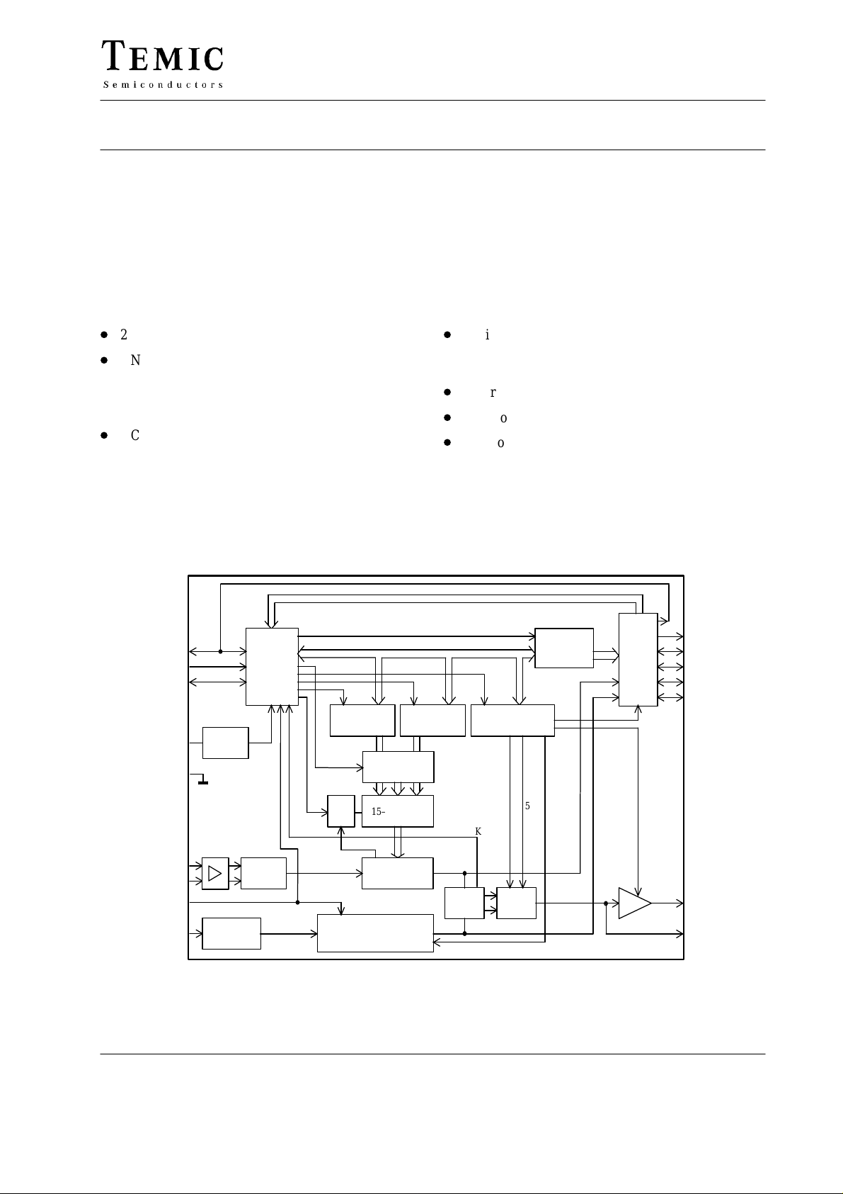
This IC contains an integrated preamplifier, a high
frequency prescaler, a reference divider with multiple
programmable divider ratios, a crystal oscillator, a phase/
frequency detector together with a charge pump, a tuning
amplifier and an analog-to-digital converter.
D
3-wire bus mode:
4 unidirectional ports (open collector)
Lock output (open collector)
D
Programmable reference divider
D
Low power consumption (typ. 5 V / 23 mA)
D
Electrostatic protection according to MIL-STD 883
U6239B
Block Diagram
AS / ENABLE / P3
RDS / AMS
SCL
SDA
GND15
RFi
XTAL
10
5
4
Power–on
12 Vs
reset
14
13
3
2
Oscillator
UNI–BUS
Control
POR
div. by 16
Prescaler
14–bit Shift Reg.
15–bit Latch
Sync
Sync
AMS
SET
RDS
divide by 256/512/off/1024
divide by 25/50/140/250
divide by 50/100/280/500
15/14–bit
counter
11
5–bit Latch
T1
RD1,2,3
FP
FR
LOCK
Phase
detector
7–bit Latch
T0 5I
Charge
pump
8–bit Latch7–bit Latch
ADC
I/O
Ports
OS
9611809
9
8
7
6
16VD
1PD
P0/Lock
P4
P5
P6 / ADC
P7
TELEFUNKEN Semiconductors
Rev . A3, 28-May-97
Figure 1.
1 (15)
Page 2
U6239B
Á
Á
Á
Á
Á
Á
Ordering Information
Extended Type Number Package Remarks
U6239B-AFPG3 SO16, plastic package Taped and reeled
SSO16 package on request
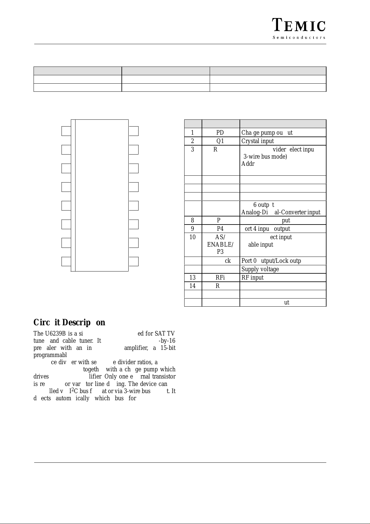
Pin Configuration
Pin Symbol Function
PD
Q1
RDS/AMS
SDA
SCL
P7
P6/ ADC
P5
1
2
3
4
5
6
7
8
95 10947
VD
16
GND
15
RFi
14
RFi
13
V
S
12
P0/ Lock
11
AS/ENABLE/
10
P3
P4
9
1
2
PD
Q1
3 RDS/
AMS
4
5
6
7
Á
8
9
10
Á
SDA
SCL
P7
P6/
ÁÁÁ
ADC
P5
P4
AS/
ENABLE/
ÁÁÁ
P3
11
12
13
14
15
16
P0/Lock
V
RFi
RFi
GND
VD
Charge pump output
Crystal input
Reference divider select input
(3-wire bus mode)
Address mode select input
(I
Data input/ output
Clock input
Port 7 input/ output
Port 6 output
Analog-Digital-Converter input
Port 5 input/ output
Port 4 input/ output
Address select input
Enable input
Port 3 output
Port 0 output/Lock output
S
Supply voltage
RF input
RF input
Ground
Active filter output
2
C bus mode)
ББББББББ
ББББББББ
Circuit Description
The U6239B is a single-chip PLL designed for SAT TV
tuner and cable tuner. It consists of a divide-by-16
prescaler with an integrated preamplifier, a 15-bit
programmable divider, a crystal oscillator, and a
reference divider with selectable divider ratios, a phase/
frequency detector together with a charge pump which
drives the tuning amplifier. Only one external transistor
is required for varactor line driving. The device can be
controlled via I
detects automatically which bus format has been
received. Therefore, there is no need for a bus selection
pin. In I
or one fixed and three programmable I
depending on the voltage level at Pin 3. They are
2 (15)
2
C bus format or via 3-wire bus format. It
2
C bus mode, the device has four programmable
2
C bus addresses,
programmed by applying a specific input voltage to the
address select input Pin 10, enabling the use of up to four
synthesizers in a system. If the fixed address is used, this
pin can be used as a normal output port. The same pin
serves as the enable signal input in 3-wire bus mode.
Depending whether the fixed address is used or not there
are five or six open collector outputs for switching
functions available. In 3-wire bus mode there are four
open collector outputs and one lock signal output. All
open collector outputs are capable of sinking at least
2
10 mA. In I
C bus mode an analog-to-digital converter
(ADC) is available for digital AFC (automatic frequency
control) applications and the ports P4, P5 and P7 can also
be used as input ports.
TELEFUNKEN Semiconductors
Rev . A3, 28-May-97
Page 3
U6239B
Á
Á
Á
Á
Á
Á
Á
Á
Á
Á
Á
Functional Description
The U6239B is programmed via a 2-wire I2C bus or
3-wire bus depending on the received data format. In
2
C bus mode the three bus input pins 4, 5, 10 are used as
I
SDA, SCL and address select inputs or in 3-wire bus
mode as date, clock and enable inputs, respectively. The
data include the scaling factor SF and port output
information. In I
functions available (ADC, bidirectional ports, etc.)
Oscillator frequency calculation :
f
VCO
: Locked frequency of voltage controlled oscillator
f
vco
SPF : Scaling factor of programmable divider (15 bit in
2
C bus mode, 14 bit in 3-wire bus mode)
I
SRF : Scaling factor of reference divider
(B25/B50/B140/B250/B256/B512/B1024
in I
B
280/B500 in 3-wire bus mode)
: Reference oscillator frequency:
f
refosc
3.2/ 4 MHz crystal or external reference
frequency (max. 8 MHz)
The input amplifier together with a divide-by-16
prescaler provides excellent sensitivity (see “Typical
2
C bus mode there are some additional
= 16 SPF f
2
C bus mode, B25/B50/B100/B140/B250
refosc
/SRF
prescaler input sensitivity”). The input impedance is
shown in the diagram “Typical input impedance”. When
a new divider ratio is entered according to the requested
, the phase detector and charge pump adjusts the
f
VCO
control voltage of the VCO together with the tuning
amplifier until the output signals of the programmable
divider and the reference divider are in frequency locked
and phase locked. The reference frequency may be provided by an external source, capacitively coupled into
Pin 2, or by using an on-board crystal with an 18 pF capacitor in series. The crystal operates in the series
resonance mode. The reference divider division ratio
is selectable to B25/ B50/ B140/ B250/ B256/ B512/
2
B
1024 in the I
B
140/ B250/ B280/ B500 in the 3-wire bus mode.
C bus mode and B25/ B50/ B100/
In I2C bus mode, the division ratio may be set via three
bits, in 3-wire bus mode via two bits and a voltage at the
reference divider select input Pin 3. In addition, there are
port outputs available for band switching and other
purposes.
Application
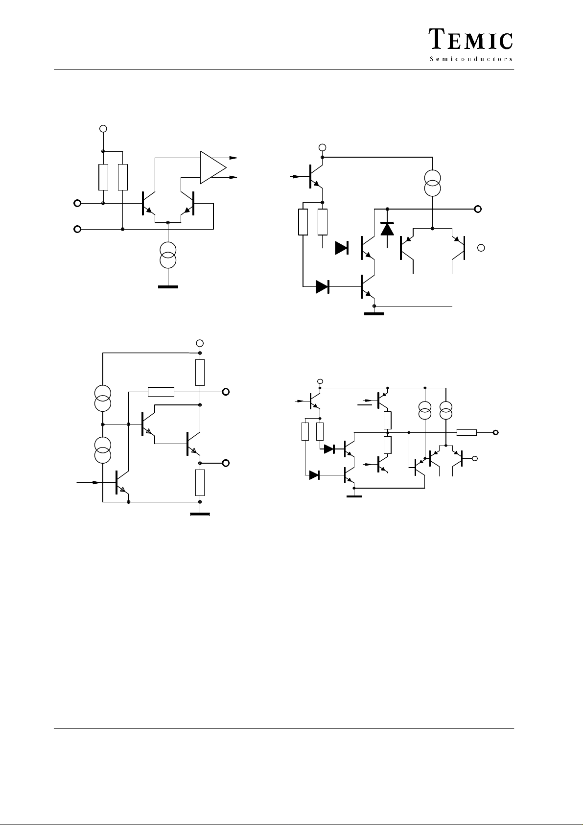
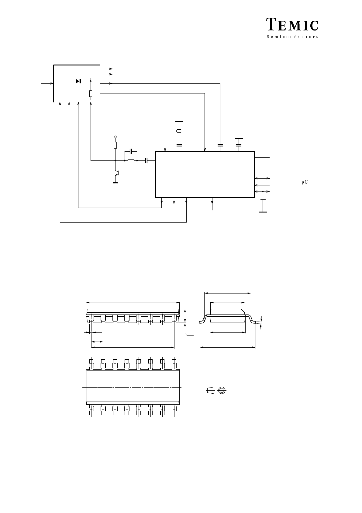
A typical application is shown on page 14. All input/
output interface circuits are shown on the pages 12 and
13. Some special features which are related to test- and
alignment procedures for tuner production are explained
together with the bus mode descriptions.
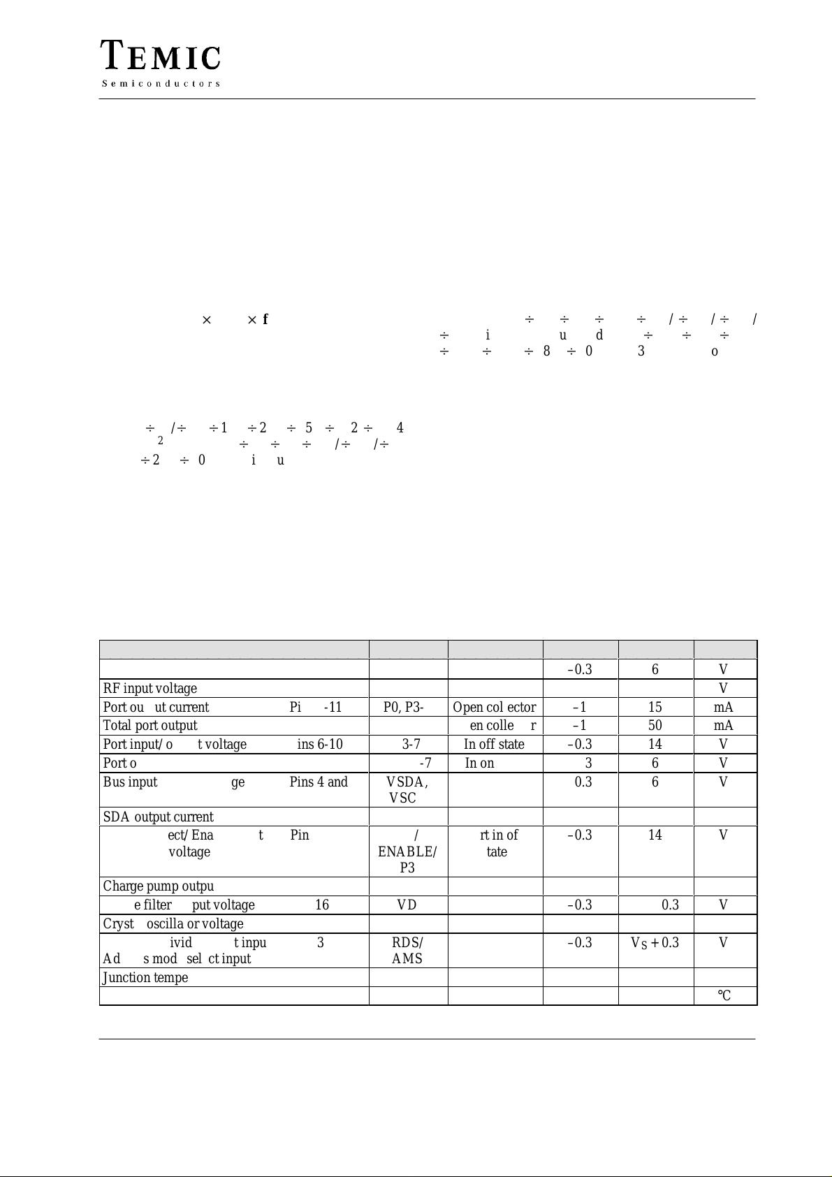
Absolute Maximum Ratings
All voltages are referred to GND (Pin 15)
Parameters Symbol Conditions Min. Max. Unit
Supply voltage Pin 12
RF input voltage Pins 13, 14
Port output current Pins 6-11
Total port output current Pins 6-11
Port input/ output voltage Pins 6-10
Port output voltage Pins 6-11
Bus input/ output voltage Pins 4 and 5
ББББББББББББ
SDA output current Pin 4
Address select/ Enable input Pin 10
Port output voltage
ББББББББББББ
Charge pump output voltage Pin 1
Active filter output voltage Pin 16
Crystal oscillator voltage Pin 2
Reference divider select input/ Pin 3
Address mode select input
Junction temperature T
Storage temperature T
P0, P3-7
P0, P3-7
P0, P3-7
VSDA,
ÁÁ
ENABLE/
ÁÁ
Vs
RFi
P3-7
VSCL
ISDA
AS/
P3
PD
VD
Q1
RDS/
AMS
j
stg
–0.3
–0.3
Open collector
Open collector
In off state
In on state
ÁÁÁÁÁÁÁ
Open collector
Port in off
state
ÁÁÁÁ
–1
–1
–0.3
–0.3
–0.3
–1
–0.3
ÁÁ
–0.3
–0.3
–0.3
–0.3 V
–40 125 °C
–40 125 °C
6
Vs + 0.3
15
50
14
6
6
ÁÁÁ
5
14
ÁÁÁ
Vs + 0.3
Vs + 0.3
Vs + 0.3
+ 0.3 V
S
V
V
mA
mA
V
V
V
ÁÁ
mA
V
ÁÁ
V
V
V
TELEFUNKEN Semiconductors
Rev . A3, 28-May-97
3 (15)
Page 4
U6239B
Á
Á
Á
Á
Á
Á
Á
Á
Á
Á
Á
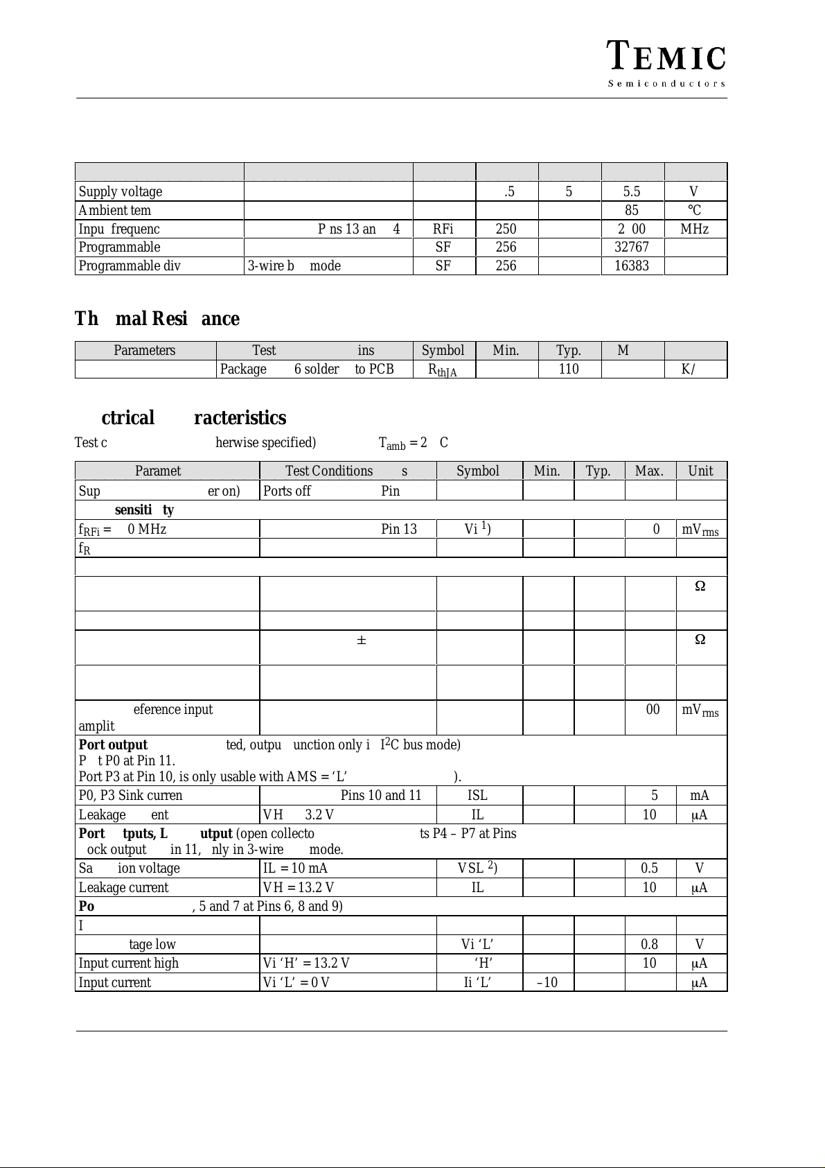
Operating Range
All voltages are referred to GND (Pin 15)
Parameters Test Conditions / Pins Symbol Min. Typ. Max. Unit
Supply voltage
Ambient temperature
Input frequency
Programmable divider
Programmable divider
I2C bus mode
3-wire bus mode
Thermal Resistance
Parameters Test Conditions / Pins Symbol Min. Typ. Max. Unit
Junction ambient Package SO16 soldered to PCB R
Electrical Characteristics
Test conditions (unless otherwise specified): V
Parameters Test Conditions / Pins Symbol Min. Typ. Max. Unit
Supply current (prescaler on)
Input sensitivity
f
= 250 MHz
RFi
f
= 750 -2900 MHz
RFi
Crystal oscillator
Recommended crystal series
ББББББББ
resistance
Crystal oscillator drive level
Crystal oscillator source
ББББББББ
impedance
External reference input
frequency
External reference input
ББББББББ
amplitude
Port outputs (current limited, output function only in I2C bus mode)
Port P0 at Pin 11.
Port P3 at Pin 10, is only usable with AMS = ‘L’ (= 3 address mode).
P0, P3 Sink current VH = 12 V, Pins 10 and 11 ISL 0.7 1 1.5 mA
Leakage current VH = 13.2 V IL 10
Port outputs, Lock output (open collector, locked = ‘L’. Ports P4 – P7 at Pins 6–9)
Lock output at Pin 11, only in 3-wire bus mode.
Saturation voltage IL = 10 mA VSL 2) 0.5 V
Leakage current VH = 13.2 V IL 10
Port inputs (Ports 4, 5 and 7 at Pins 6, 8 and 9)
Input voltage high Vi ‘H’ 2.7 V
Input voltage low Vi ‘L’ 0.8 V
Input current high Vi ‘H’ = 13.2 V Ii ‘H’ 10
Input current low Vi ‘L’ = 0 V Ii ‘L’ –10
Ports off Pin 12
БББББББÁÁÁÁÁÁÁ10ÁÁÁÁ
Nominal spread " 15%
БББББББ
AC coupled sinewave
AC coupled sinewave
БББББББ
Pin 12
Pins 13 and 14
= 5 V, T
S
amb
Pin 13
Pin 13
Pin 2
Pin 2
Pin 2
Pin2
V
T
RFi
SF
SF
S
amb
thJA
4.5
–20
250
256
256
5
110 K/W
= 25°C
ICC
Vi 1)
Vi 1)
ÁÁÁÁÁÁ
100
20
2
ÁÁÁÁÁÁ70ÁÁÁÁ
23
50
–650
ÁÁ
5.5
85
2900
32767
16383
300
300
200
ÁÁÁÁ
8
200
V
°C
MHz
mA
mV
mV
ÁÁ
mV
MHz
mV
ÁÁ
m
m
m
m
rms
rms
W
rms
W
rms
A
A
A
A
4 (15)
TELEFUNKEN Semiconductors
Rev . A3, 28-May-97
Page 5
U6239B
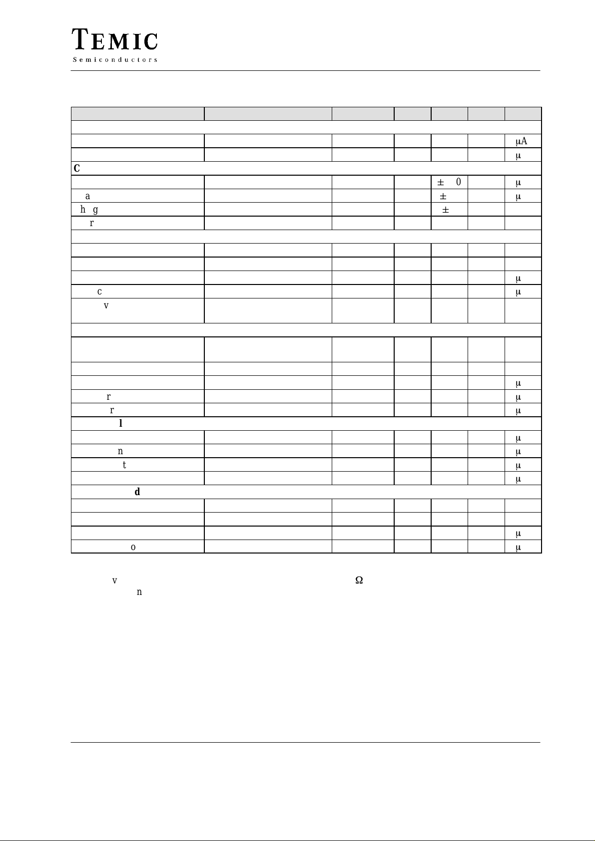
Electrical Characteristics (continued)
Parameters Test Conditions / Pins Symbol Min. Typ. Max. Unit
ADC input (ADC, Pin 7, see page 8 for ADC-levels)
Input current high Vi ‘H’ = 13.2 V Ii ‘H’ 10
Input current low Vi ‘L’ = 0 V Ii ‘L’ –10
Charge pump output (PD)
Charge pump current ‘H’ 5I = 1, VPD = 1.7 V, Pin 1 IPDH
Charge pump current ‘L’ 5I = 0, VPD = 1.7 V, Pin 1 IPDL
Charge pump leakage current T0 = 1, VPD = 1.7 V, Pin 1 IPDTRI
Charge pump amplifier gain Pins 1 and 16 6400
Bus inputs Data and Clock (SDA, SCL) I2C bus mode and 3-wire bus mode
Input voltage high Pins 4 and 5 Vi ‘H’ 3 5.5 V
Input voltage low Pins 4 and 5 Vi ‘L’ 1.5 V
Input current high Vi ‘H’ = VS, Pins 4 and 5 Ii ‘H’ 10
Input current low Vi ‘L’ = 0 V, Pins 4 and 5 Ii ‘L’ –20
Output voltage SDA
(open collector)
Bus input Enable, 3-wire bus mode (ENABLE, Pin 10)
Input voltage high Pin 10 Vi ‘H’ 75%
Input voltage low Pin 10 Vi ‘L’ 1.0 V
Input current high Vi ‘H’ = VS, Pin 10 Ii ‘H’ 10
Input current low (RDS = ‘L’) Vi ‘L’ = 0 V, Pin 10 Ii ‘L’ –10
Input current low (RDS = ‘H’) Vi ‘L’ = 0 V, Pin 10 Ii ‘L’ –100
Address selection / port output (AS/P3, Pin 10)
Input current low (AMS = L) Vi ‘L’ = 0 V (3 address) Ii ‘L’ –10
Input current high (AMS = L) Vi ‘H’ = 13.2 V (3 address) Ii ‘H’ 10
Input current low (AMS = H) Vi ‘L’ = 0 V (4 address) Ii ‘L’ –100
Input current high (AMS = H) Vi ‘H’ = VS (4 address) Ii ‘H’ 10
Reference divider select/Address mode select (RDS, AMS)
Input voltage high Pins 4 and 5 Vi ‘H’ 3 5.5 V
Input voltage low Pins 4 and 5 Vi ‘L’ 1.5 V
Input current high Vi ‘H’ = VS, Pins 4 and 5 Ii ‘H’ 10
Input current low Vi ‘L’ = 0 V, Pins 4 and 5 Ii ‘L’ –20
ISDA‘L’ = 3 mA, Pin 4 VSDA ‘L’ 0.4 V
V
"
180
"
50
"
5 nA
VS +
S
0.3 V
m
A
m
A
m
A
m
A
m
A
m
A
V
m
A
m
A
m
A
m
A
m
A
m
A
m
A
m
A
m
A
Notes:
1
) RMS - voltage calculated from the measured available power on 50 W.
2
) T ested with one port active. The collector voltage of an active port must not exceed 6 V.
TELEFUNKEN Semiconductors
Rev . A3, 28-May-97
5 (15)
Page 6
U6239B
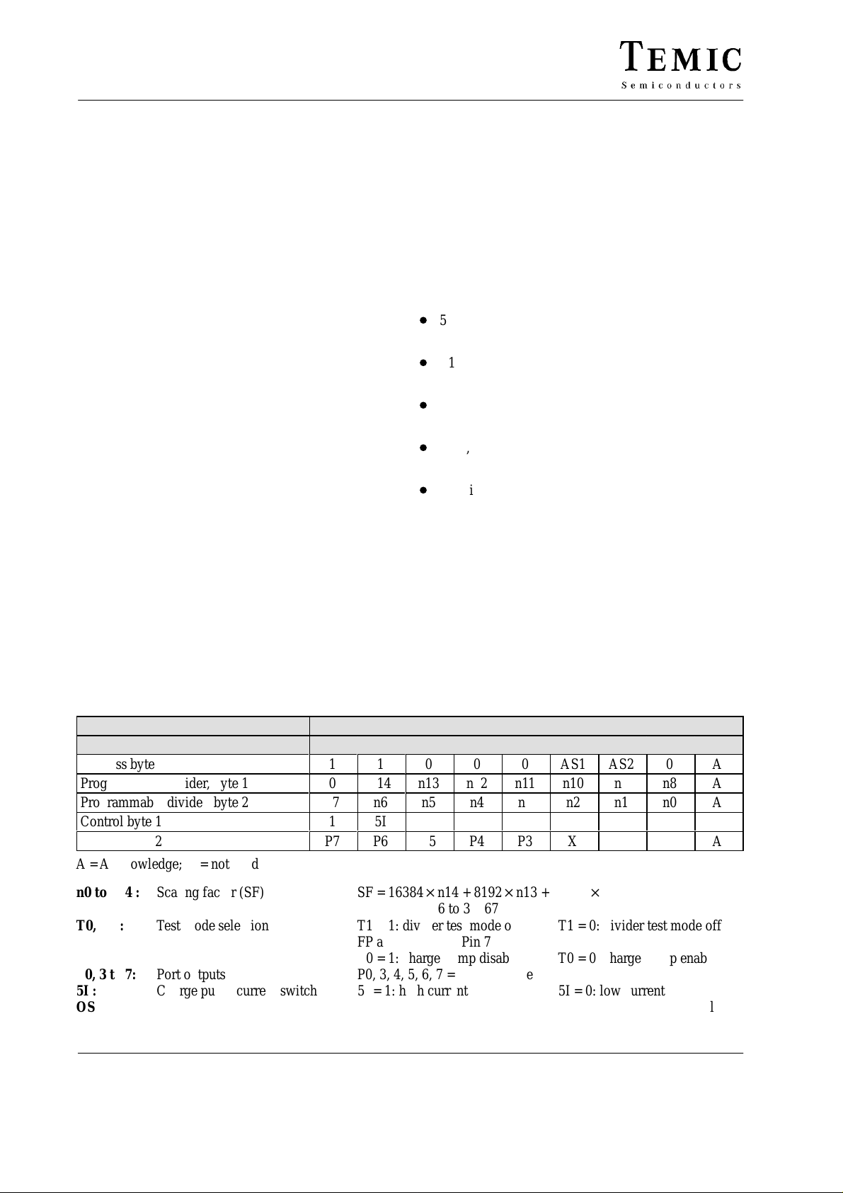
I2C Bus Description
Functional Description
When the U6239B is controlled via a 2-wire I2C bus
format, then data and clock signals are fed into the SDA
and SCL lines respectively. Depending on the LSB of the
address byte, the device can either accept new data (write
mode: LSB = 0) or send data (read mode: LSB = 1).
Depending on the voltage at the address mode select
input, the device has one fixed and three programmable
or four programmable I
2
“I
C bus write data format” and “I2C bus read data
format” describe the format of the data and show how to
select the device addresses by applying the appropriate
voltages at address select Pin 10 and the address mode
select Pin 3.
Write Mode (Address byte LSB = 0)
When write mode is activated and the correct address byte
is received, the SDA line is pulled low by the device
during the acknowledge period. The SDA line is also
pulled low during the acknowledge periods, when additional data bytes are programmed. After the address
transmission (first byte), data bytes can be sent to the device. There are four data bytes requested to fully program
the device. Once the correct address is received and acknowledged, the first bit of the following byte determines
whether that byte is interpreted as byte 2 or 4; a logic 0 for
divider information and a logic 1 for control and port output information. If byte 2 has been received, the device
always expects byte 3 next. Likewise if byte 4 has been
received, byte 5 is expected. Additional data bytes can be
entered without the need to re-address the device until an
2
C bus stop condition is recognized. This allows a
I
2
C bus addresses. The tables
smooth frequency sweep for fine tuning AFC purposes.
The table “I
sible data transfer examples. In addition, the stop
condition is not a must, the device may be programmed
by using the start condition only.
The programmable divider bytes PDB1 and PDB2 are
stored in a 15-bit latch and control the division ratio of the
15-bit programmable divider. The control byte CB1 enables the controlling of the following special functions:
D
5I bit switches between low and high charge pump
current
D
T1 bit enables divider test mode when it is set to
logic 1
D
T0 bit enables the charge pump to be disabled when
it is set to logic 1
D
RD3, 2 and 1 - bits enable selection of the reference
divider ratio
D
OS-bit disables the charge pump drive amplifier output when it is set to logic 1.
The charge pump current can only be controlled in I
bus mode. In 3-wire bus mode, the high charge pump current is always active.
The OS-bit function disables the complete PLL function.
This enables the tuner alignment by supplying the tuning
voltage directly through the 30 V supply voltage of the
tuner. The control byte CB2 programs the port outputs P0
and P3 - 7.
2
C bus pulse diagram” provides some pos-
2
C
Description I2C Bus Data Format
MSB LSB
Address byte
Programmable divider, byte 1
Programmable divider, byte 2
Control byte 1
Control byte 2
A = Acknowledge; X = not used
n0 to n14 : Scaling factor (SF) SF = 16384 n14 + 8192 n13 + ... + 2 n1 + n0
T0, T1 : Test mode selection T1 = 1: divider test mode on, T1 = 0: divider test mode off
P0, 3 to 7: Port outputs P0, 3, 4, 5, 6, 7 = 1: port active
5I : Charge pump current switch 5I = 1: high current 5I = 0: low current
OS : Output switch OS = 1: varicap drive disable OS = 0: varicap drive enable
6 (15)
1
0
n7
1
P7
1
n14
n6
5I
P6
SF - range: 256 to 32767
FP at Pin 6, FR at Pin 7
T0 = 1: charge pump disable T0 = 0: charge pump enable
0
n13
n5
T1
P5
0
n12
n4
T0
P4
0
AS1
n11
n3
RD3
P3
n10
n2
RD2
TELEFUNKEN Semiconductors
AS2
n9
n1
RD1
X
X
Rev . A3, 28-May-97
0
n8
n0
OS
P0
A
A
A
A
A
Page 7
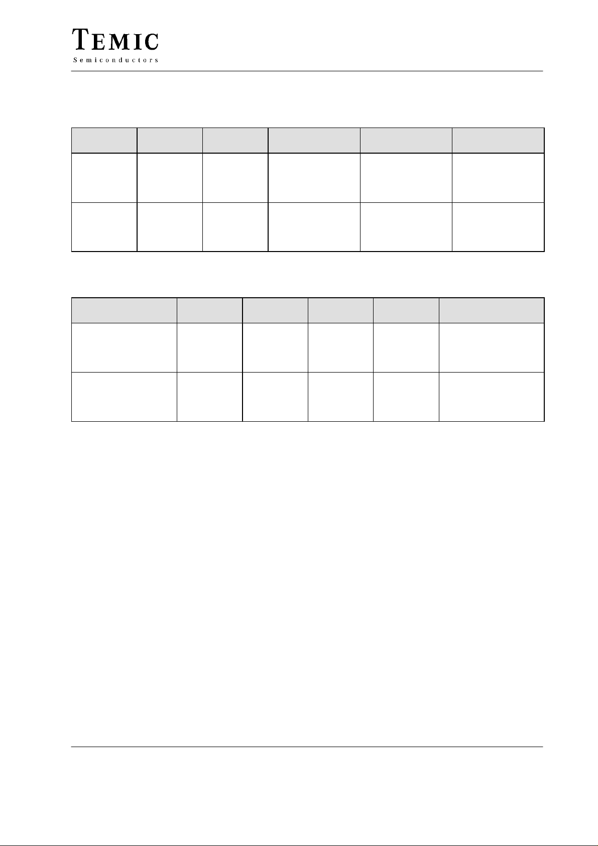
I2C Bus Description (continued)
Reference divider selection RD1, RD2, RD3:
U6239B
RD3 RD2 RD1 Reference
1
1
1
1
0
0
0
0
* when a 4MHz crystal is used
Address selection AS1, AS2, AMS:
AMS
Voltage at Pin 3
< 0.8 V or open
< 0.8 V or open
< 0.8 V or open
< 0.8 V or open
> 2.4
> 2.4
> 2.4
> 2.4
0
0
1
1
0
0
1
1
AS1 AS2 Address Dec. Value Voltage at Pin 10
0
1
0
1
0
1
0
1
0
0
1
1
0
0
1
1
0
1
0
1
0
1
0
1
Divider Ratio
1024
off
256
512
140
25
250
50
C0
C2
C4
C6
C0
C2
C4
C6
Frequency
Step Size*
62.5 kHz
–
250 kHz
125 kHz
457.14 kHz
2560 kHz
256 kHz
1280 kHz
192
194
196
198
192
194
196
198
Max. Operating
Frequency*
2.047 GHz
–
2.9 GHz
2.9 GHz
2.9 GHz
2.9 GHz
2.9 GHz
2.9 GHz
0 to 10% V
always valid
40 to 60% V
90% VS to 13.2 V
0 to 10% V
40 to 60% V
90% VS to V
S
S
S
open
S
S
Read Mode (Address byte LSB = 1)
After the address transmission (first byte), the status byte
can be read from the device on the SDA line (MSB first).
Data is valid on the SDA line during logic high of the SCL
signal. The controller accepting the data has to pull the
SDA line to low-level during all status-byte acknowledge
periods to read another status byte. If the controller fails
to pull the SDA line to low-level during this period, the
device will then release the SDA line to allow the
controller to generate a STOP condition.
The POR bit (power-on-reset) is set to a logic 1 when the
supply voltage V
(at 25°C) and also when the device is initially turned on.
The POR bit is reset to a logic 0 when the read sequence
is terminated by a STOP condition. When the POR bit is
set high (at low V
of the device has dropped below 3 V
S
), this indicates that all the
S
programmed information is lost and the port outputs are
all set to high impedance state.
The FL bit indicates whether the loop is in phase lock
condition (logic 1) or not (logic 0).
If the ADC or the ports are to be used as inputs, the
corresponding outputs must be programmed to a high
impedance state (logic 1).
The bits I2, I1 and I0 show the status of the I/O ports P7,
P5 and P4 respectively. A logic 0 indicates a LOW level
and a logic 1 a HIGH level (TTL levels).
The bits A2, A1 and A0 represent the digital information
of the 5-level ADC. This converter can be used to feed
AFC information to the controller from the IF section of
the receiver, as shown in the typical application circuit on
page 14.
TELEFUNKEN Semiconductors
Rev . A3, 28-May-97
7 (15)
Page 8
U6239B
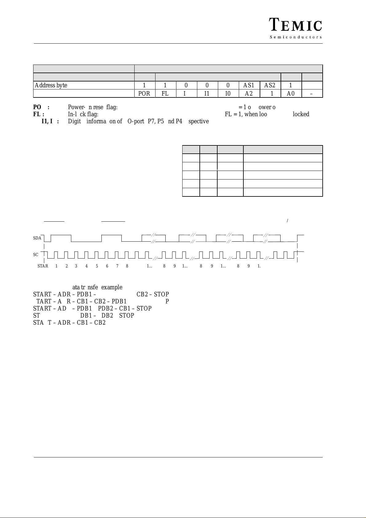
I2C Bus Description (continued)
Description I2C Bus Read Data Format
MSB LSB
Address byte
Status byte
POR : Power-on reset flag: POR = 1 on power on
FL : In-lock flag: FL = 1, when loop is phase locked
I2, I1, I0 : Digital information of I/O-ports P7, P5 and P4 respectively
A2, A1, A0 : Digital data of the 5-level ADC. see next table
1
POR
1
FL
I2
0
I1
0
I0
0
AS1
A2
AS2
A1
1
A0
A
–
A/D Converter Levels:
I2C Bus Pulse Diagram
/ A /
Address byte
SDA
SCL
STAR T 1 2 3 4 5 6 7 8
Data transfer examples
START – ADR – PDB1 – PDB2 – CB1 – CB2 – STOP
START – ADR – CB1 – CB2 – PDB1 – PDB2 – STOP
START – ADR – PDB1 – PDB2 – CB1 – STOP
START – ADR – PDB1 – PDB2 – STOP
START – ADR – CB1 – CB2 – STOP
START – ADR – CB1 – STOP
1.Byte / A /2.Byte
9
81... 9 81... 9 1... 8 9 1... 8 STOP9
A2 A1 A0 Input voltage to ADC Pin 9
1
/ A /
0
0
1
Á0Á1ÁÁ0ББББББББ
0
0
0
0
0
60% Vs to 13.2 V
1
45% to 60% Vs
30% to 45% Vs
1
15% to 30% Vs
0
0 V to 15% Vs
/ A /3.Byte 4.Byte / A /
9611811
Description
START = Start condition
ADR = Address byte
PDB1 = Programmable divider byte 1
PDB2 = Programmable divider byte 2
CB1 = Control byte 1
CB2 = Control byte 2
STOP = Stop condition
8 (15)
TELEFUNKEN Semiconductors
Rev . A3, 28-May-97
Page 9
I2C Bus Description (continued)
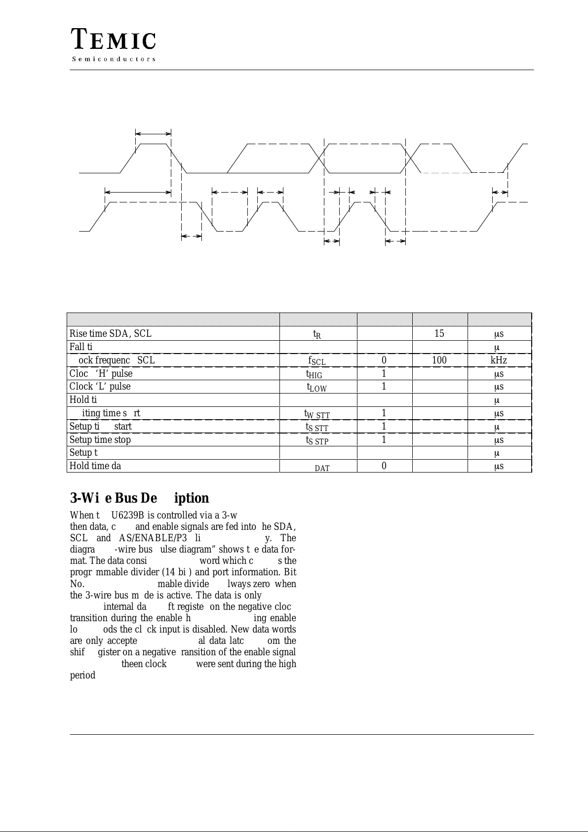
I2C Bus Timing
t
W STT
SDA
U6239B
9611812
t
SCL
START CLOCK DATACHANGE STOP
Rise time SDA, SCL
Fall time SDA, SCL
Clock frequency SCL
Clock ‘H’ pulse
Clock ‘L’ pulse
Hold time start
Waiting time start
Setup time start
Setup time stop
Setup time data
Hold time data
t
H STT
tt t
HIGHLOWS STT
Figure 2.
R F S STP
t
t
t
H DATS DAT
t
Parameters Symbol Min. Max. Unit
t
R
t
F
f
SCL
t
HIGH
t
LOW
t
H STT
t
W STT
t
S STT
t
S STP
tS
DAT
t
H DAT
0
1
1
1
1
1
1
0.25
0
15
15
100
m
m
kHz
m
m
m
m
m
m
m
m
s
s
s
s
s
s
s
s
s
s
3-Wire Bus Description
When the U6239B is controlled via a 3-wire bus format,
then data, clock and enable signals are fed into the SDA,
SCL and AS/ENABLE/P3 lines respectively. The
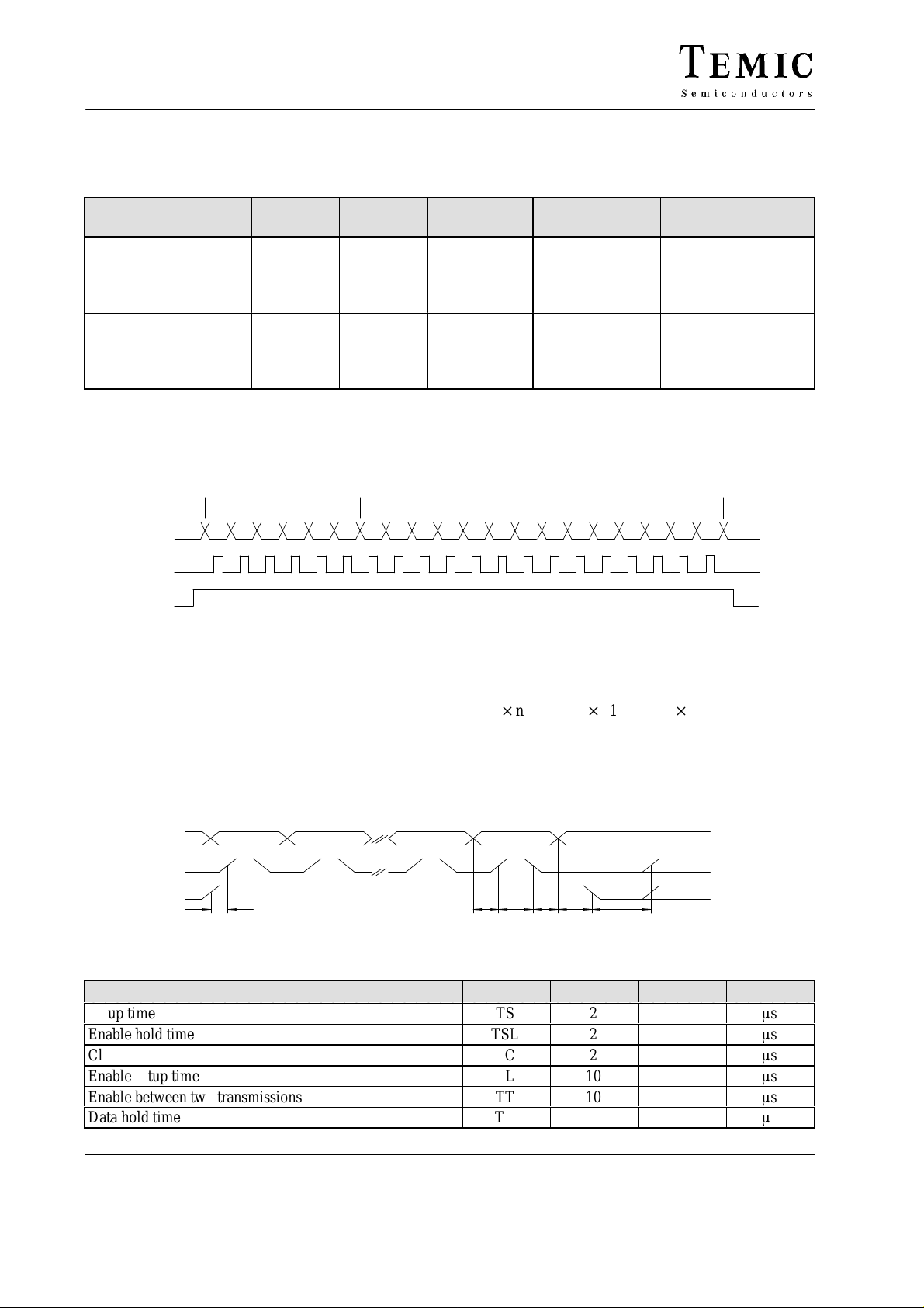
diagram “3-wire bus pulse diagram” shows the data format. The data consist of a single word which contains the
programmable divider (14 bit) and port information. Bit
No. 15 of the programmable divider is always zero, when
the 3-wire bus mode is active. The data is only clocked
into the internal data shift register on the negative clock
transition during the enable high period. During enable
low periods the clock input is disabled. New data words
are only accepted by the internal data latches from the
shift register on a negative transition of the enable signal
if exactly eigtheen clock pulses were sent during the high
period of the enable. The data sequence and the timing is
described in the following diagrams.
TELEFUNKEN Semiconductors
Rev . A3, 28-May-97
In 3-wire bus mode Pin 9 automatically becomes the
lock-signal output. An improved lock detect circuit
generates a flag when the loop has attained lock. ‘In lock’
is indicated by a low impedance state (on) of the open
collector output.
In 3-wire bus mode the high charge pump current is
always active. The charge pump current can only be con-
2
trolled in I
C bus mode.
The complete PLL function can be disabled by
programming a normally not used division ratio of zero.
This allows the tuner alignment by supplying the tuning
voltage directly through the 33 V supply voltage of the
tuner.
In 3-wire bus mode the division ratio of the reference
divider is controlled via information RD1, RD2 and the
reference divider select input Pin 3.
9 (15)
Page 10
U6239B
3-Wire Bus Description (continued)
Reference divider selection RD1, RD2, RDS:
RDS Voltage at
RD2 RD1 Reference
Pin 3
0 to 10% VS or open
0 to 10% V
0 to 10% V
0 to 10% V
90 to 100% V
90 to 100% V
90 to 100% V
90 to 100% V
or open
S
or open
S
or open
S
S
S
S
S
* when a 4-MHz crystal is used
3-Wire Bus Pulse Diagram
4 Port bits/ 2 Ref.Div. bits
RD1 RD2
P5
SDA
SCL
ENABLE
Frequency
Divider Ratio
0
0
1
1
0
0
1
1
P6P4
0
1
0
1
0
1
0
1
MSB
P7
n13 n0
280
50
500
100
140
25
250
50
14-bit scaling factor SF
Step Size*
228.57 kHz
1280 kHz
128 kHz
640 kHz
457.14 kHz
2560kHz
256 kHz
1280 kHz
Maximum Operating
Frequency*
2.9 GHz
2.9 GHz
2.097 GHz
2.9 GHz
2.9 GHz
2.9 GHz
2.9 GHz
2.9 GHz
LSB
9611813
Figure 3.
n0 to n13 Scaling factor (SF) SF = 8192 n13 + 4096 n12 + ... +2 n1 + n0
SF - Range: 256..16383
P4 to P7 Port outputs P4 - P7 = 1: port active
RD1, RD2 Reference divider selection see table above
3-Wire Bus Timing
Data
Clock
Enable
TL
Figure 4.
Parameters Symbol Min. Max. Unit
Setup time
Enable hold time
Clock width
Enable setup time
Enable between two transmissions
Data hold time
LSB
TS
TSL
TC
TL
TT
TH
THTS
TSLTC
TT
9611880
2
2
2
10
10
2
m
s
m
s
m
s
m
s
m
s
m
s
10 (15)
TELEFUNKEN Semiconductors
Rev . A3, 28-May-97
Page 11
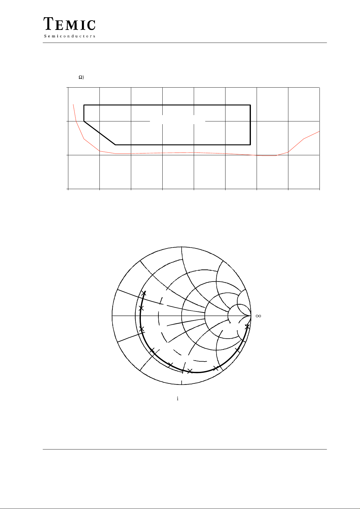
Typical Prescaler Input Sensitivity
U6239B
Vi (mV
1000
100
10
on 50 W)
rms
1
0
500 1000 1500
Typical Input Impedence
Operating window
2000 2500
Frequency (MHz)
j
3000 3500
4000
9611877
0.2j
0
–0.2j
0.5j
0.2
–0.5j
4.0 GHz
3.5 GHz
0.5
3.0 GHz
2.5 GHz
1
2.0 GHz
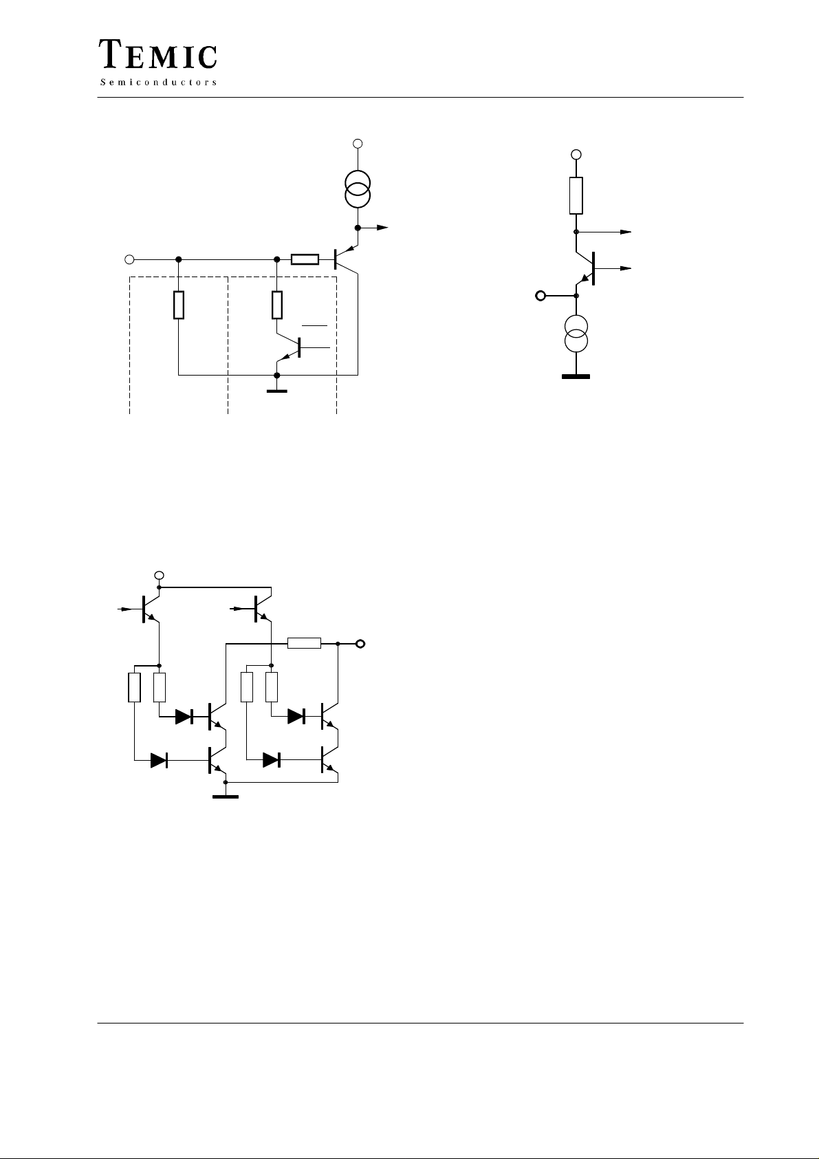
1.5 GHz
–j
Figure 5.
2
500 MHz
1 GHz
2j
5
100MHz
–2j
Z = 5 0
0
5j
1
–5j
Ω
9611878
TELEFUNKEN Semiconductors
Rev . A3, 28-May-97
11 (15)
Page 12
U6239B
Input/ Output Interface Circuits
Vref
Vs
RF1
RF2
1.5k
OS
1.5k
Figure 6. RF input
60
(O/P Disable)
2k
45k
9611853
PD
VD
Port
Vref
9611856
Figure 8. Ports P4, P5, P6, P7
Vs
P3
AMS
AMS
125k
375k
12k
AS / P3
ENABLE
Vref
9611857
12 (15)
Figure 7. Loop amplifier
9611854
Figure 9. Address select/ Enable input/ Port output P3
TELEFUNKEN Semiconductors
Rev . A3, 28-May-97
Page 13
U6239B
SDA/SCL/RDS/AMS
40 k
20
SDA onlyRDS/AMS only
Figure 10. SCL/SDA and RDS/AMS input
3 k
ACK
V
96 11855
S
Vs
XTAL Q1
9611858
Figure 11. Reference oscillator
P0
Vs
Lock
Figure 12. Port P0/ Lock output
12k
Port P0/Lock
9611810
TELEFUNKEN Semiconductors
Rev . A3, 28-May-97
13 (15)
Page 14
U6239B
Application Circuit
SAT–Tuner
f
SAT
f
IF
f
VCO
AFC
22k
Package Information
Package SO16
Dimensions in mm
33V
22n
39k
10.0
9.85
RDS/AMS
100n
4 MHz
ADC
18 p
1
16
P5P7 P0 / Lock
U6239B
9
86
P4
1 n
7
11
Figure 13.
5.2
4.8
3.7
RFi
1 n
141323
9611879
12
15
4
5
10
Vs
GND
SDA
from/to mC
SCL
AS / ENABLE / P3
100 p
14 (15)
1.4
0.4
1.27
8.89
16 9
18
0.25
0.10
3.8
6.15
5.85
technical drawings
according to DIN
specifications
TELEFUNKEN Semiconductors
0.2
13036
Rev . A3, 28-May-97
Page 15

U6239B
Ozone Depleting Substances Policy Statement
It is the policy of TEMIC TELEFUNKEN microelectronic GmbH to
1. Meet all present and future national and international statutory requirements.
2. Regularly and continuously improve the performance of our products, processes, distribution and operating systems
with respect to their impact on the health and safety of our employees and the public, as well as their impact on
the environment.
It is particular concern to control or eliminate releases of those substances into the atmosphere which are known as
ozone depleting substances (ODSs).
The Montreal Protocol ( 1987) and its London Amendments (1990 ) intend to severely restrict the use of ODSs and
forbid their use within the next ten years. Various national and international initiatives are pressing for an earlier ban
on these substances.
TEMIC TELEFUNKEN microelectronic GmbH semiconductor division has been able to use its policy of
continuous improvements to eliminate the use of ODSs listed in the following documents.
1. Annex A, B and list of transitional substances of the Montreal Protocol and the London Amendments respectively
2. Class I and II ozone depleting substances in the Clean Air Act Amendments of 1990 by the Environmental
Protection Agency (EPA) in the USA
3. Council Decision 88/540/EEC and 91/690/EEC Annex A, B and C (transitional substances) respectively.
TEMIC can certify that our semiconductors are not manufactured with ozone depleting substances and do not contain
such substances.
We reserve the right to make changes to improve technical design and may do so without further notice.
Parameters can vary in different applications. All operating parameters must be validated for each customer
application by the customer. Should the buyer use TEMIC products for any unintended or unauthorized
application, the buyer shall indemnify TEMIC against all claims, costs, damages, and expenses, arising out of,
directly or indirectly, any claim of personal damage, injury or death associated with such unintended or
unauthorized use.
TEMIC TELEFUNKEN microelectronic GmbH, P.O.B. 3535, D-74025 Heilbronn, Germany
Telephone: 49 (0)7131 67 2831, Fax number: 49 (0)7131 67 2423
TELEFUNKEN Semiconductors
Rev . A3, 28-May-97
15 (15)
 Loading...