

Page 1
Three-Tone Ringer for Telephone Sets
Description
The three-tone ringing integrated circuit U4076B, in
conjunction with a piezo transducer or loudspeaker
replaces the normal electromechanical telephone bell. It
is operated with the ringing current from the exchange.
Features
D
Three-tone ringing sequence with 800 Hz, 1067 Hz
and 1333 Hz
D
Sequence frequency adjustable between 2.5 Hz and
25 Hz
D
Adjustable volume
D
Push-pull output stage
D
Piezo transducer or loudspeaker connection
D
Common input for frequency and call recognition
There is also a possibility of operating the IC with the dc
supply voltage, being developed for large operating
range. The integrated circuit is overload protected.
D
Clock oscillator with ceramic resonator or LC series
cct possible
D
Input protective diode
D
On-chip rectifier bridge
D
Protection circuit against ringing in a parallel circuit
Benefit
U4076B
D
Reduced pulse duration for electromagnetic
transducers
22 F
m
4 (5) 6 (7) 10 (11) 8 (9)
7
5
Frequency
1
Three
state
a
~
~
b
m
0.8 F
R
2.2 k
L
W
(8)
(6)
14
(16)
(1)
Supply
Frequency
monitoring
W
600 k
Level
monitoring
Reset
b
D
Suitable for German Post Office Specification,
FTZ 121671 Pfl. 3, edition dated 24.03.82
W
43 k 4.7 nF
Tone sequence
oscillator
96 ms
127 ms
Divider
128:1
Divider
32:1
Divider
(10)9 (15) 13
Divider
2:1
Divider
14:1
Tone signal
generator
32:1
Reset
a
Ground: output signal
Open: output signal
Clock signal
generator
93 7792 e
12
(13)
11
(12)
2 (2)
3 (3)
100 k
log
455 kHz
W
Case: DIP14 or SO16-L (Pin connections for SO 16-L case in bracket)
TELEFUNKEN Semiconductors
Rev . A1, 15-May-96
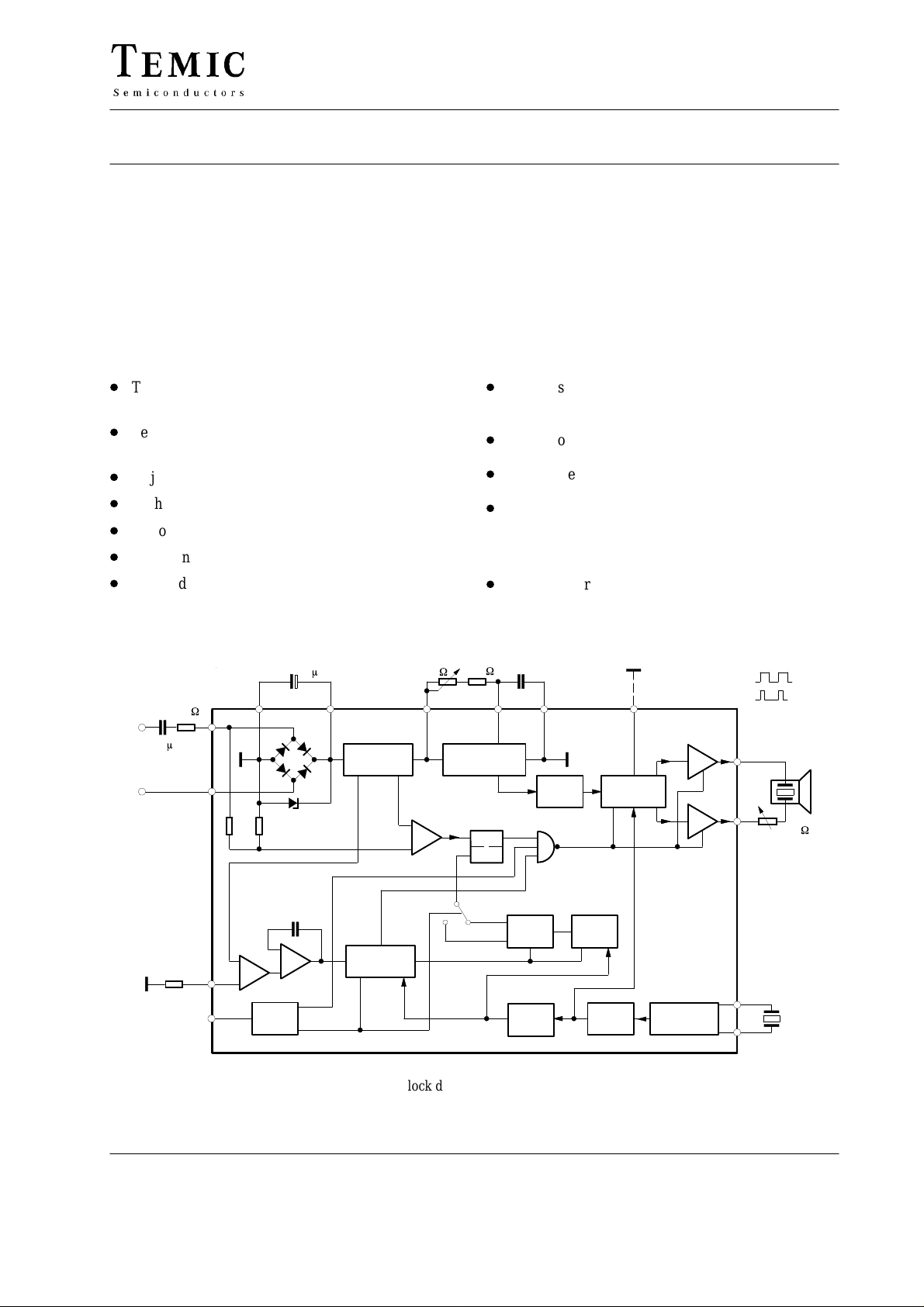
Figure 1. Block diagram and application circuit
1 (6)
Preliminary Information
Page 2
U4076B
Pin Description
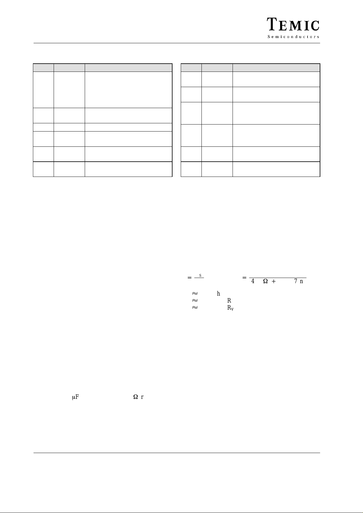
Pin Symbol Function
1 (1) Frequency monitoring
Open: 23 to 54 Hz
Ground: 12 to 54 Hz
With Pin 6 (7) connected:
Switched off
2, 3
(2, 3)
4 (5) Ground
5, 7
(6, 8)
6 (7) Charging capacitor, C
(8, 9,
10)
Clock signal generator
Power supply
bridge rectifier
Frequency oscillator
for
L,
Pin Connections and Functional
Description Including External
Circuitry
Pin 1: Frequency monitoring
Frequency is monitored via Pin 1. The following possibilities are available (three-state logic):
a) Pin 1 is open: ringing frequency is between 23 and
54 Hz.
b) Pin 1 is grounded: ringing frequency is between 12
and 54 Hz.
c) Pin 1 is connected to Pin 6 (7): ringing frequency has
no influence (dc operation)
Pins 2 and 3 (2, 3): Clock signal generator
A ceramic resonator for a frequency of 455 kHz must be
connected between Pin 2 (2) and Pin 3 (3). The clock
frequency of the generator is used for three-tone ringing
sequence and control signals for frequency identification.
Pin 4 (5): Ground
Reference point for all voltages.
Pins 5, 6 and 7 (6, 7, 8): Power supply
Pins 5 (6) and 7 (8) connect the circuit with a ringing ac
supplied by the exchange via lines a and b. A decoupling
capacitor of 1 mF in series with 2.2 kW resistance is
needed for overvoltage protection and the insertion loss
requirement of the German Post Office specifications.
The supplied ac current is rectified by the on-chip bridge
circuit. The rectified current charges the capacitor on
Pin 6 (7), which supplies the dc voltage for the integrated
Pin Symbol Function
8, 9,
10
(9, 10,
11)
11, 12
(12,
13)
13
(15)
14
(16)
(4,
14)
circuit. Instead of a ringing ac current supplied by the exchange, the IC can be driven by a dc voltage applied
directly to terminals 6 (7) (+) and 4 (5) (–). An integrated
Z diode limits the maximum supply voltage range up to
27 V.
Tone sequence
Frequency oscillator
Output signals
Output signal shape
Open = short pulse width
Ground = 1:1
Load resistance, R
Not connected
L
Pins 8, 9 and 10 (9, 10, 11):
Sequence frequency adjustment
The sequence of the three-tone ringing frequency (800,
1067 and 1333 Hz) is determined by the external network
calculated as follow:
f
OSC
+
f
2
if: k 0.95 then R
if: k 1 then R
if: k 1.2 then R
The sequence frequency adjustment is determined by the
frequency prescaler ratio in the IC.
192
whereas f
OSC
v
v
v
+
(43 kW)
= 0 to 20 kΩ
= 30 to 150 kΩ
> 200 kΩ
IC
R
)47nF
V
Pins 11 and 12 (12, 13): Output signal
The three-tone ringing sequence of 800 Hz, 1067 Hz and
1333 Hz is realized if the clock oscillator is synchronised
with a ceramic resonator of 455 kHz between Pins 2 (2)
and Pin 3 (3). This gives excellent tone frequency and
eliminates complicated frequency setting procedures.
The output signal without load is (2 V
output stage transducers in BTL configuration can process an average current of up to 20 mA, whereas a short
time current of 40 mA is possible in both direction when
t = 0.1 ms. An external current limitation is necessary
when the IC is operating with voltage between Pin 6(7)
and Pin 4 (5). The tone sequence always starts at the
lower frequency.
6(7)
– 2.5) V
pp.
The
2 (6)
TELEFUNKEN Semiconductors
Rev . A1, 15-May-96
Preliminary Information
Page 3
U4076B
Pin 13 (15): Output signal shape
Output signal has different duty cycles according to the
position of Pin 13 (15). When grounded it has a duty cycle
of 1:1. When using a dynamic loudspeaker (activation via transformer/capacitor), a reduced signal
is recommended. This can be achieved by connecting a
capacitor greater than 1 nF between Pin 13 (15) and
ground.
Pin 14 (16): Switched on/off
Switched on/off is controlled by Pin 14 (16). The dc
voltage on the charge capacitor between Pin 4 (5) and 6
(7) is loaded a dummy load as long as the tone ringing is
not switched-on. In on-position (amplitude and frequency
recognition), Pin 14 (16) is connected internally with
15
10 mF
2 kV
110
W
Pin 4 (5) and the dummy load is switched-off. In
off-position, Pin 14 (16) is connected with Pin 6 (7)
internally and the dummy load is switched on.
Overload protection
The integrated circuit can withstand an ac voltage of
110 V / 50 Hz for 15 seconds between terminals a and b.
The circuit will not be damaged by a surge voltage test
with the following conditions:
93 7575 e
= 2 kV
cs
Charging voltage of surge capacitance: V
Pulse shape: 10/700 µs
Pulse sequence: 30 s
No of surges: 10
Polarity change after five surges
W
25
0.22 mF
W
a
Tone ringing
Figure 1
b
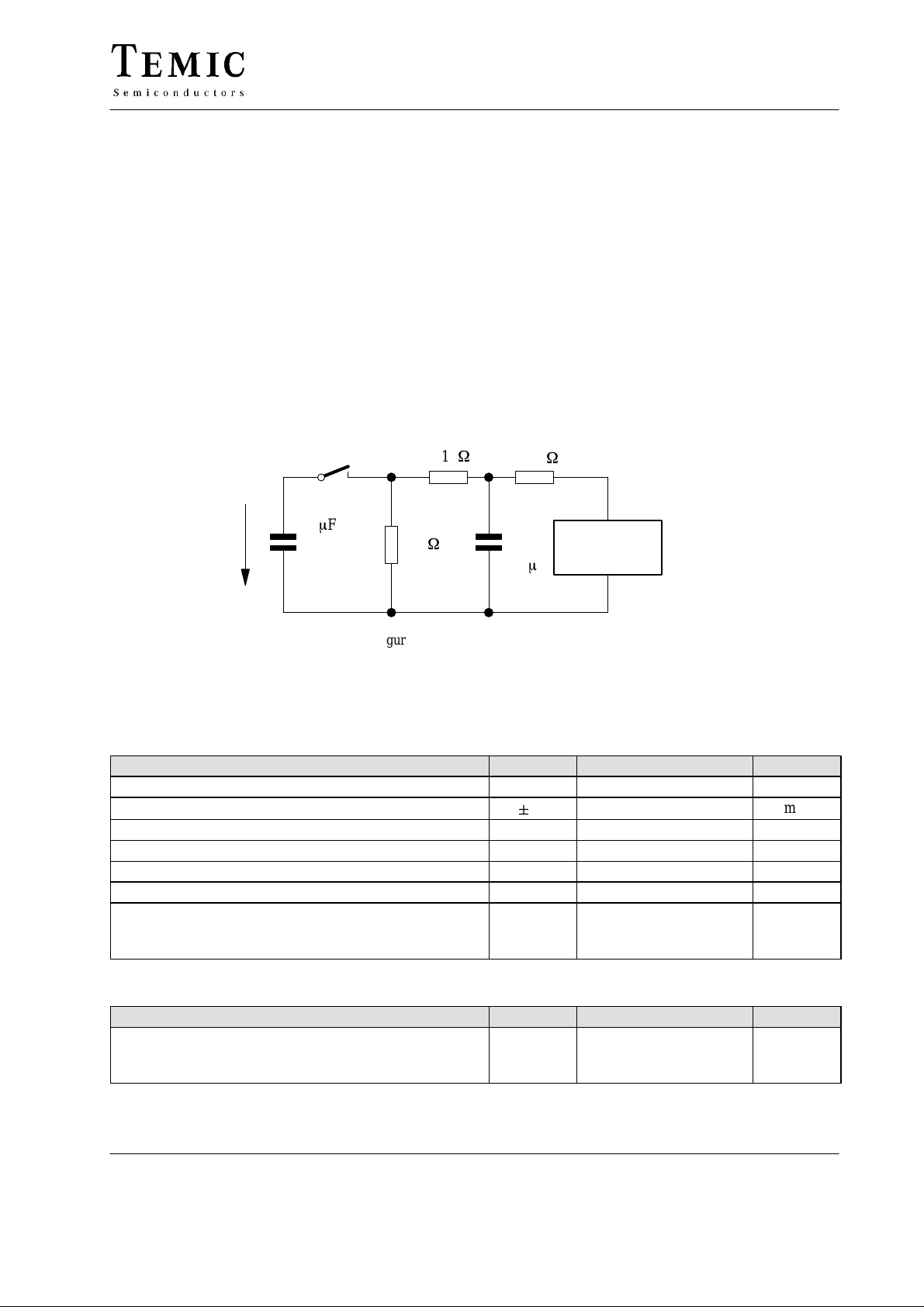
Figure 2. Surge voltage test circuit
Absolute Maximum Ratings
Reference point Pin 4 (5) unless otherwise specified
Parameters Symbol Value Unit
Supply current Pins 5 and 7 (6, 8) I
Output current Pins 11 and 12 (12, 13)
Junction temperature T
Ambient temperature range T
Storage temperature range T
Power dissipation
T
= 60 °C
amb
DIP14
SO16-L
Thermal Resistance
Parameters Symbol Value Unit
Junction ambient
DIP14
SO16-L
"
R
R
amb
stg
P
P
thJA
thJA
tot
tot
S
I
0
j
50 mA
50 mA
125 °C
–25 to +60 °C
–40 to +125 °C
860
720
75
90
mW
mW
K/W
K/W
TELEFUNKEN Semiconductors
Rev . A1, 15-May-96
3 (6)
Preliminary Information
Page 4
U4076B
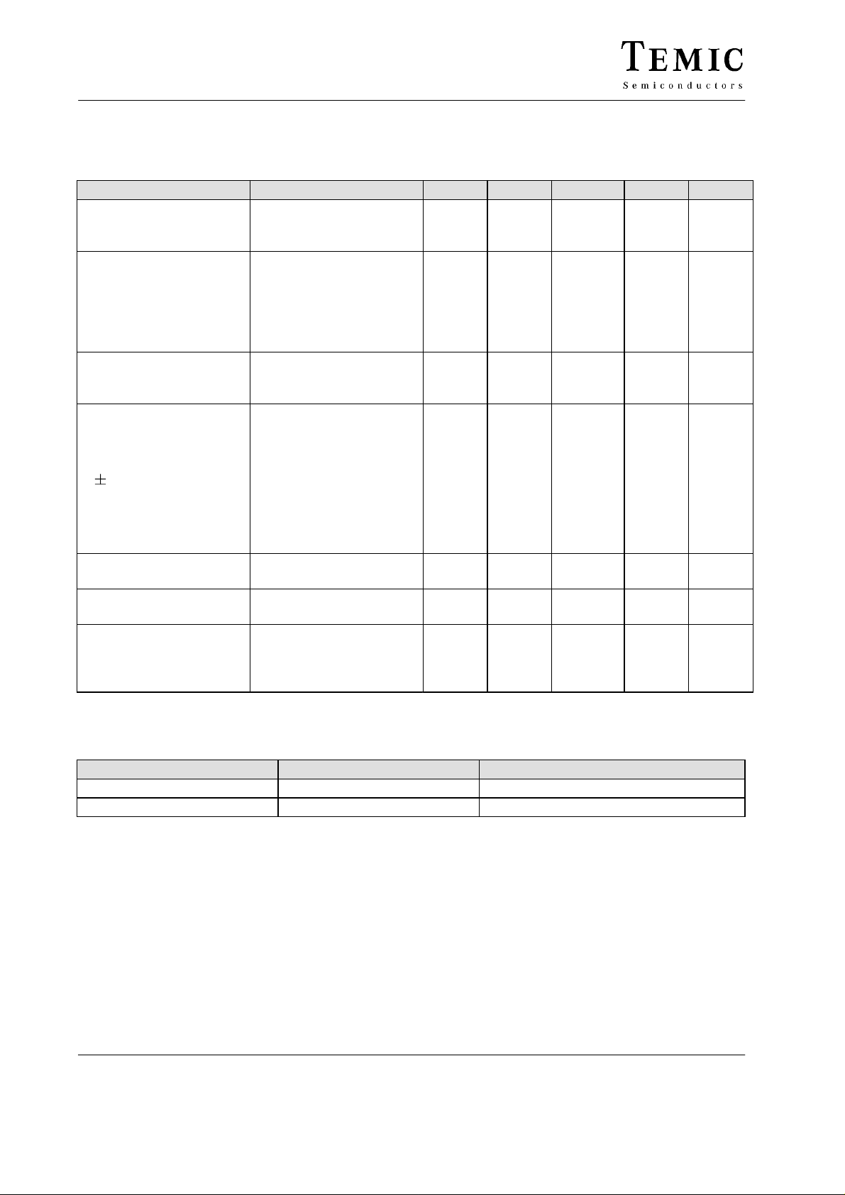
Electrical Characteristics
V
S
= 10 V, f
= 455 kHz,T
clock
Parameters Test Conditions / Pins Symbol Min. Typ. Max. Unit
Supply current (no load)
outputs open V
= +25°C
T
amb
6(7)
= 10 V
Frequency range of the
ringing input current
a) Pin 1 - open
b) Pin 1 - grounded
c) Pin 1 - connected to
Pin 6 (7)
AC-operation
Switch-on threshold
Switch-off threshold
DC-operation
Switch-on threshold
Switch-off threshold
Output on resistances
20 mA
at
Output signal frequency
Build-up time of clock
oscillator
Internal voltage limitation
=1 mA
I
Z
Repetition rate oscillator:
Low state
High state
Allowable resistor
= 25 to 60°C. Reference point Pin 4 (5), Pin 13 (15) ground, unless otherwise specified.
amb
Pins 5 and 7 (6)
I
S
0.9 1.15 1.3 mA
Pins 5 and 7 (6, 8)
23 to 54
f
ring
12 to 54
DC
operation
Pin 6 (7) 6.5
Pin 6 (7)
Pin 6 (7)
Pin 11 (12)
Pin 12 (13)
Pins 11 and 12 (12,13)
V
6–4 (7–5)
3.5
2.75
2.0
R
on
R
on
f
0
f
1
f
2
f
3
t
B
448/455
800/812
1067/1083
1333/1354
10 ms
25 27 30 V
8.5
5.5
4.75
4.0
400
400
Pin 6 (7)
Pin 8 (9)
Pin 8 (9)
Pins 8-10 (9-11)
V
8(9)
V
8(9)
R
0.5
0.043
0.6
2.0
0.7
2
Hz
V
V
V
W
W
kHz
Hz
Hz
Hz
V
V
MΩ
Ordering Information
Extended Type Number Package Remarks
U4076B-FL SO16
U4076B DIP14
4 (6)
TELEFUNKEN Semiconductors
Preliminary Information
Rev . A1, 15-May-96
Page 5
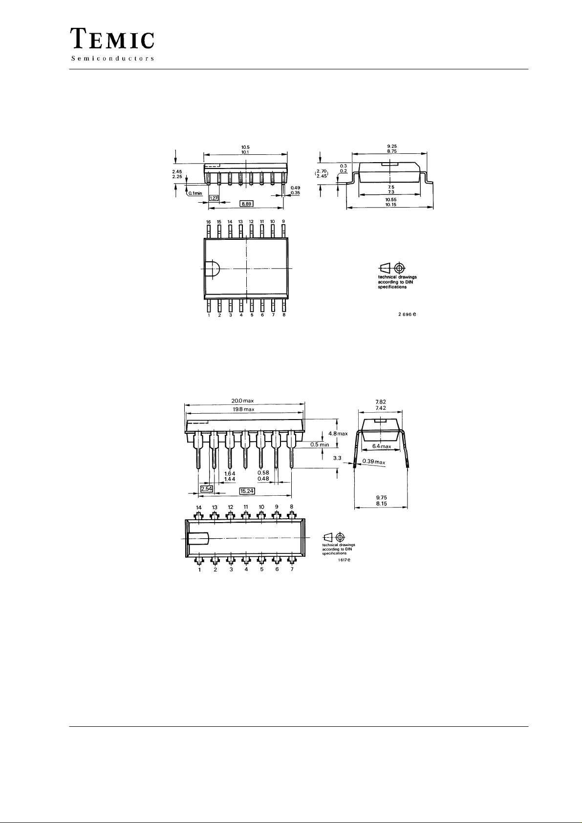
Dimensions in mm
Package: SO16-L
U4076B
Package: DIP14
TELEFUNKEN Semiconductors
Rev . A1, 15-May-96
5 (6)
Preliminary Information
Page 6

U4076B
Ozone Depleting Substances Policy Statement
It is the policy of TEMIC TELEFUNKEN microelectronic GmbH to
1. Meet all present and future national and international statutory requirements.
2. Regularly and continuously improve the performance of our products, processes, distribution and operating systems
with respect to their impact on the health and safety of our employees and the public, as well as their impact on
the environment.
It is particular concern to control or eliminate releases of those substances into the atmosphere which are known as
ozone depleting substances (ODSs).
The Montreal Protocol ( 1987) and its London Amendments (1990) intend to severely restrict the use of ODSs and
forbid their use within the next ten years. Various national and international initiatives are pressing for an earlier ban
on these substances.
TEMIC TELEFUNKEN microelectronic GmbH semiconductor division has been able to use its policy of
continuous improvements to eliminate the use of ODSs listed in the following documents.
1. Annex A, B and list of transitional substances of the Montreal Protocol and the London Amendments respectively
2. Class I and II ozone depleting substances in the Clean Air Act Amendments of 1990 by the Environmental
Protection Agency (EPA) in the USA
3. Council Decision 88/540/EEC and 91/690/EEC Annex A, B and C (transitional substances) respectively.
TEMIC can certify that our semiconductors are not manufactured with ozone depleting substances and do not contain
such substances.
We reserve the right to make changes to improve technical design and may do so without further notice.
Parameters can vary in different applications. All operating parameters must be validated for each customer
application by the customer. Should the buyer use TEMIC products for any unintended or unauthorized
application, the buyer shall indemnify TEMIC against all claims, costs, damages, and expenses, arising out of,
directly or indirectly, any claim of personal damage, injury or death associated with such unintended or
unauthorized use.
6 (6)
TEMIC TELEFUNKEN microelectronic GmbH, P.O.B. 3535, D-74025 Heilbronn, Germany
Telephone: 49 (0)7131 67 2831, Fax number: 49 (0)7131 67 2423
TELEFUNKEN Semiconductors
Rev . A1, 15-May-96
Preliminary Information
 Loading...