

Page 1
查询U2894B供应商
Modulation PLL for GSM, DCS and PCS Systems
Description
The U2894B is a monolithic integrated circuit. It is
realized using TEMIC’s advanced silicon bipolar UHF5S
technology. The device integrates a mixer, an I/Q modulator, a phase-frequency detector (PFD) with two
synchronous programmable dividers, and a charge pump.
The U2894B is designed for cellular phones such as
GSM900, DCS1800, and PCS1900, applying a
transmitter architecture at which the VCO operates at the
TX output frequency. No duplexer is needed since the outof-band noise is very low. The U2894B exhibits low
power consumption. Broadband operation gives you high
flexibility for multi-band frequency mappings. The IC is
available in a shrinked small-outline 28-pin package
(SSO28).
The U2893B offers the same functionality with other
divider ratios.
Electrostatic sensitive device.
Observe precautions for handling.
U2894B
Features
D
Supply voltage range 2.7 V to 5.5 V
D
Current consumption 50 mA
D
Power-down functions
D
High-speed PFD and charge pump (CP)
D
Small CP saturation voltages (0.5/0.6 V)
D
Programmable dividers and CP polarity
D
Low-current standby mode
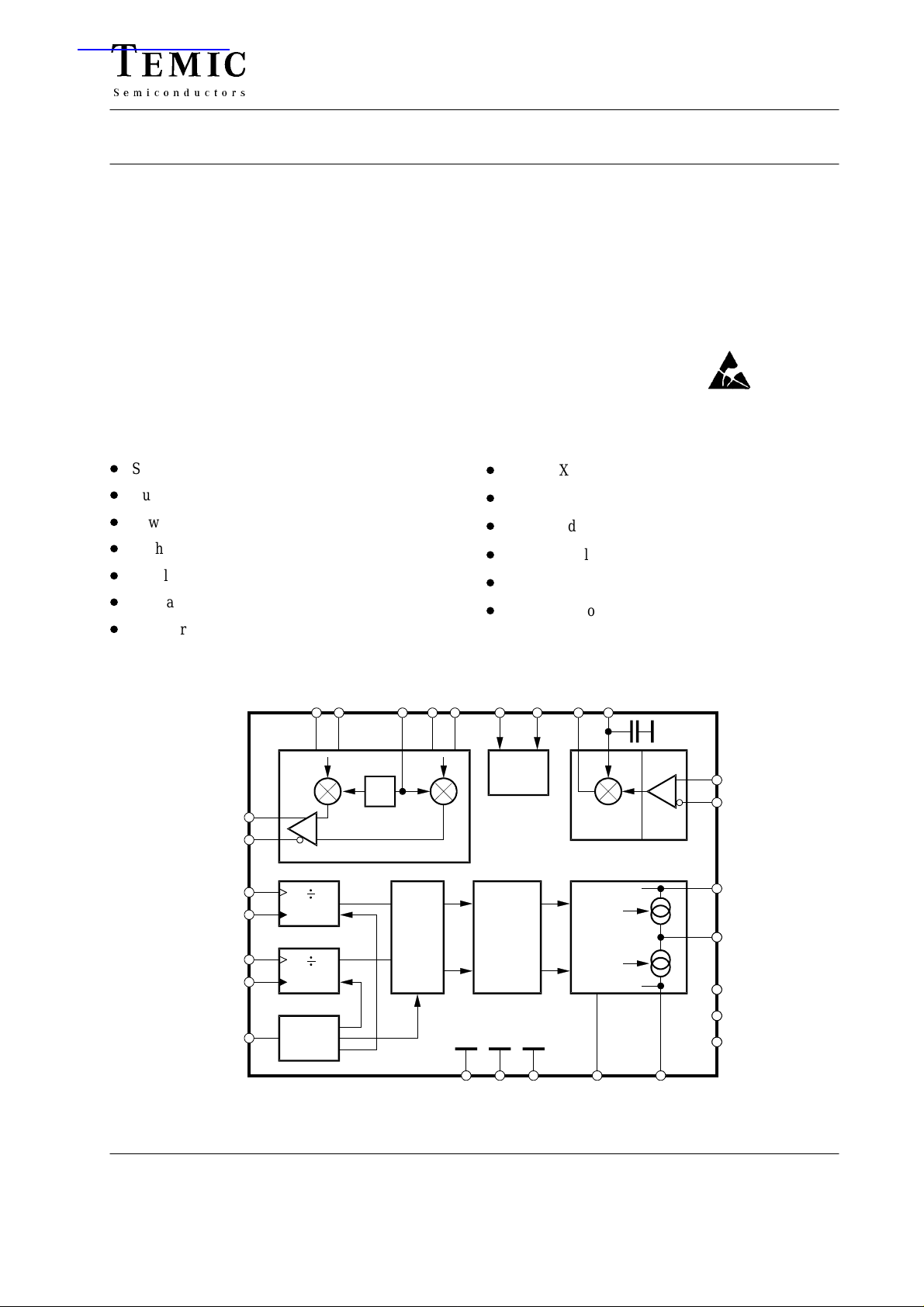
Block Diagram
I NI MDLO Q NQ PUMIX PU MIXO MIXLO
ND
RD
MC
5
6
16
17
13
14
15
+
N1
divider
R1
divider
Mode
control
MDO
NMDO
NND
NRD
90°
I/Q modulator
MUX
Benefits
D
Novel TX architecture saves filter costs
D
Extended battery operating time without duplexer
D
Less board space (few external components)
D
VCO control without voltage doubler
D
Small SSO28 package
D
One device for all GSM bands
19122728321
25 20
Voltage
reference
PFD
Mixer
Charge
pump
101124184
22
23
21
26
RF
NRF
8
VSP
9
CPO
7
VS1
VS2
VS3
GND CPC GNDP
Figure 1. Block diagram
12494
Rev . A4, 30-Sep-98 1 (16)
Page 2
U2894B
ББББББББББ
ББББББББББ
ББББББББББ
ББББББББББ
ББББББББББ
ББББББББББ
ББББББББББ
ББББББББББ
ББББББББББ
ББББББББББ
ББББББББББ
ББББББББББ
ББББББББББ
ББББББББББ
ББББББББББ
ББББББББББ
Á
Á
ББББББББББ
Á
Á
ББББББББББ
ББББББББББ
ББББББББББ
ББББББББББ
ББББББББББ
ББББББББББ
ББББББББББ
ББББББББББ
Ordering Information
Extended Type Number Package Remarks
U2894B-AFSG3 SSO28 T aped and reeled
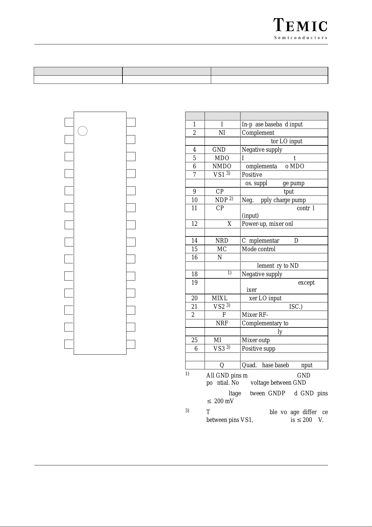
Pin Description
NI
MDLO
GND
MDO
NMDO
VS1
VSP
CPO
GNDP
CPC
PUMIX
RD
NRD
Pin Symbol Function
1
I
2
3
4
5
6
28
27
26
25
24
23
Q
NQ
VS3
MIXO
GND
NRF
10
11
1
2
3
4
5
6
7
8
9
I
NI
MDLO
GND
MDO
NMDO
VS1
VSP
CPO
GNDP
CPC
In-phase baseband input
Complementary to I
I/Q-modulator LO input
1)
Negative supply
I/Q-modulator output
Complementary to MDO
3)
Positive supply (I/Q MOD)
Pos. supply charge pump
Charge-pump output
2)
Neg. supply charge pump
Charge-pump current control
(input)
7
8
9
10
11
12
13
14
12495
Figure 2. Pinning
22
21
20
19
18
17
16
15
RF
VS2
MIXLO
PU
GND
NND
ND
MC
12
13
14
15
16
17
18
19
Á
20
21
22
23
24
25
26
27
28
1)
PUMIX
RD
NRD
MC
ND
NND
GND
PU
ÁÁÁ
MIXLO
VS2
RF
NRF
GND
MIXO
VS3
NQ
Q
Power-up, mixer only
R-divider input
Complementary to RD
Mode control
N-divider input
Complementary to ND
1)
Negative supply
Power-up, whole chip except
ББББББББ
mixer
Mixer LO input
3)
Positive supply (MISC.)
Mixer RF-input
Complementary to RF
1)
Negative supply
Mixer output
3)
Positive supply (mixer)
Complementary to Q
Quad.-phase baseband input
All GND pins must be connected to GND
potential. No DC voltage between GND pins!
2)
3)
Max. voltage between GNDP and GND pins
v
200 mV
The maximum permissible voltage difference
between pins VS1, VS2 and VS3 is v200 mV.
Rev . A4, 30-Sep-982 (16)
Page 3
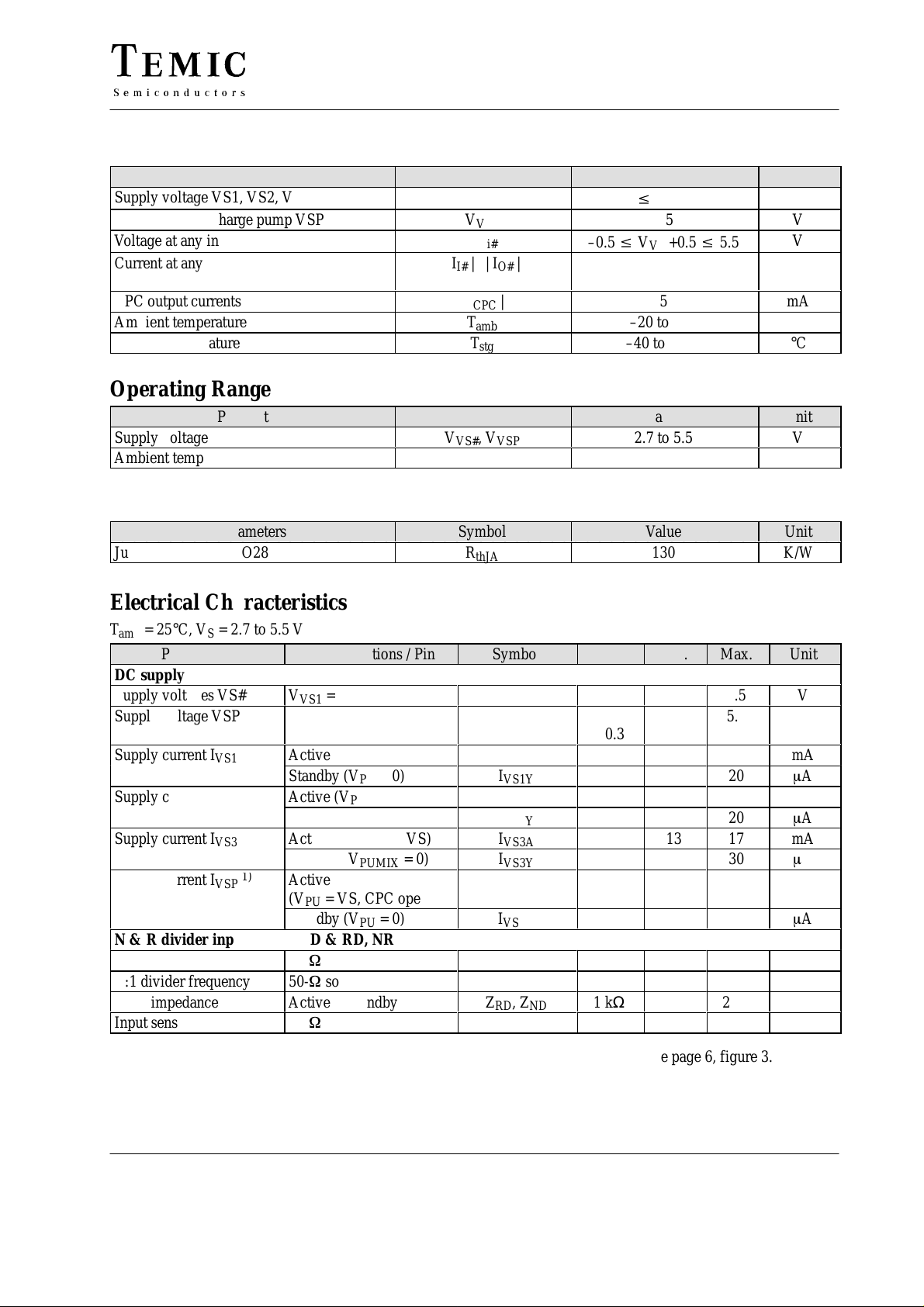
Absolute Maximum Ratings
Á
Á
Á
Á
ÁÁÁ
Á
Á
Á
ÁÁÁ
Á
Á
Á
ÁÁÁ
pp y
ÁÁÁ
pp y
ÁÁÁ
ÁÁÁ
pp y
ÁÁÁ
Á
1)
Á
Á
Á
ÁÁÁ
Á
Á
Á
Á
ÁÁÁ
ÁÁÁ
ÁÁÁ
ÁÁÁ
Parameters Symbol Value Unit
Supply voltage VS1, VS2, VS3
Supply voltage charge pump VSP
Voltage at any input
Current at any input / output pin
БББББББББББ
except CPC
CPC output currents
Ambient temperature
Storage temperature
Operating Range
Parameters Symbol Value Unit
Supply voltage
Ambient temperature
Thermal Resistance
Parameters Symbol Value Unit
Junction ambient SSO28
V
VS#
V
VSP
V
Vi#
| II# | | IO# |
ББББББ
| I
|
CPC
T
amb
T
stg
V
, V
VS#
VSP
T
amb
R
thJA
U2894B
v
V
VSP
5.5
–0.5 v V
БББББББ
+0.5 v 5.5
VS
2
5
–20 to +85
–40 to +125
2.7 to 5.5
–20 to +85
130
V
V
V
mA
ÁÁÁ
mA
°C
°C
V
°C
K/W
Electrical Characteristics
T
= 25°C, VS = 2.7 to 5.5 V
amb
Parameters T est Conditions / Pin Symbol Min. T yp. Max. Unit
DC supply
Supply voltages VS#
Supply voltage VSP
ББББББ
Supply current I
Supply current I
Supply current I
Supply current I
ББББББ
VS1
VS2
VS3
VSP
N & R divider inputs ND, NND & RD, NRD
N:1 divider frequency
R:1 divider frequency
Input impedance
Input sensitivity
V
= V
VS1
БББББББÁÁÁÁÁ
VS2
= V
Active (VPU = VS)
Standby (VPU = 0)
Active (VPU = VS)
Standby (VPU = 0)
Active (V
Standby (V
PUMIX
PUMIX
Active
(V
= VS, CPC open)
БББББББ
PU
Standby (VPU = 0)
50-W source
50-W source
Active & standby
50-W source
VS3
= VS)
= 0)
V
VS#
V
VSP
I
VS1A
I
VS1Y
I
VS2A
I
VS2Y
I
VS3A
I
VS3Y
I
VSPA
ÁÁÁÁ
I
VSPY
f
ND
f
RD
ZRD, Z
ND
VRD, V
ND
2.7
V
VS#
ÁÁ
– 0.3
ÁÁ
100
100
1 kΩ
20
5.5
5.5
ÁÁÁÁ
18
23
20
17
22
20
13
17
30
1.4
Á
1.8
ÁÁ
20
600
600
2 pF
200
V
V
ÁÁ
mA
m
A
mA
m
A
mA
m
A
mA
ÁÁ
m
A
MHz
MHz
–
mV
rms
1) Mean value measured with FND = 151 MHz, FRD = 150 MHz, current vs. time, see page 6, figure 3.
Rev . A4, 30-Sep-98 3 (16)
Page 4
U2894B
Á
Á
Á
Á
Á
Á
Á
Á
Á
Á
Á
Á
Á
4)
Á
Á
Á
Á
Á
Á
Á
Á
Á
Á
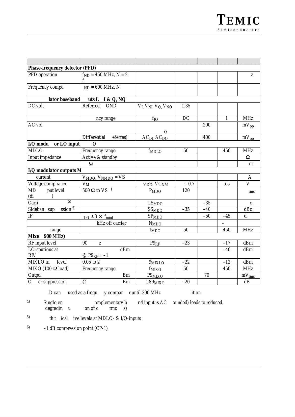
Electrical Characteristics (continued)
T
= 25°C, VS = 2.7 to 5.5 V
amb
Parameters T est Conditions / Pin Symbol Min. Typ. Max. Unit
Phase-frequency detector (PFD)
PFD operation
Frequency comparison
ББББББ
3)
only
I/Q modulator baseband inputs I, NI & Q, NQ
DC voltage
ББББББ
MD_IQ
AC voltage
ББББББ
I/Q modulator LO input MDLO
MDLO
Input impedance
Input level
I/Q modulator outputs MDO, NMDO
DC current
Voltage compliance
MDO output level
ББББББ
(differential)
Carrier suppression
Sideband suppression
IF spurious
Noise
5)
5)
Frequency range
Mixer (900 MHz)
RF input level
LO-spurious at
RF/NRF port
MIXLO input level
MIXO (100-W load)
Output level
6)
Carrier suppression
fND = 450 MHz, N = 2
fRD = 450 MHz, R = 2
fND = 600 MHz, N = 2
ББББББ
f
= 450 MHz, R = 2
RD
Referred to GND
ББББББ
Frequency range
Referred to GND
ББББББ
Differential (preferres)
Frequency range
Active & standby
50-W source
V
MDO
V
MDO
500 W to VS
ББББББ
5)
5)
fLO ± 3 f
@ 400 kHz off carrier
900 MHz
@ P9
MIXLO
@ P9RF = –15 dBm
0.05 to 2 GHz
Frequency range
@ P9
MIXLO
@ P9
MIXLO
, V
, V
NMDO
NMDO
= VS
= VC
5)
mod
= –10 dBm
= –15 dBm
= –15 dBm
f
PFD
f
V
I,
AC
AC
AC
I
MDO
MDO
P9
CS9
FD
V
NI,
f
IO
AC
I,
Q, ACNQ
AC
DI,
f
MDLO
Z
MDLO
P
MDLO
, I
NMDO
, VC
P
MDO
CS
MDO
SS
MDO
SP
MDO
N
MDO
f
MDO
P9
RF
SP9
RF
MIXLO
f
MIXO
P9
MIXO
MIXO
V
Q,
NQ
NI,
DQ
NMDOVS
БББББ
V
БББББ
БББББ
VC
БББББ
50
ÁÁÁÁÁÁÁ
1.35
Á
VS1/2
ÁÁ
DC
ÁÁÁÁ
200
225
300
VS1/2
+ 0.1
ÁÁ
1
ÁÁÁÁÁ
400
50
450
250
–11
–8
–5
2.4
– 0.7
120
Á
–32
–35
ÁÁÁÁÁ
–35
–40
–50
5.5
150
–45
–115
50
–23
450
–17
–40
–22
50
–12
450
70
–20
MHz
MHz
ÁÁ
V
ÁÁ
MHz
mV
pp
mV
pp
MHz
W
dBm
mA
V
mV
rms
ÁÁ
dBc
dBc
dBc
dBc/Hz
MHz
dBm
dBm
dBm
MHz
mV
rms
dBc
3)
4)
PFD can be used as a frequency comparator until 300 MHz for loop acquisition
Single-ended operation (complementary baseband input is AC-grounded) leads to reduced linearity
(degrading suppression of odd harmonics)
5)
6)
With typical drive levels at MDLO- & I/Q-inputs
–1 dB compression point (CP-1)
Rev . A4, 30-Sep-984 (16)
Page 5
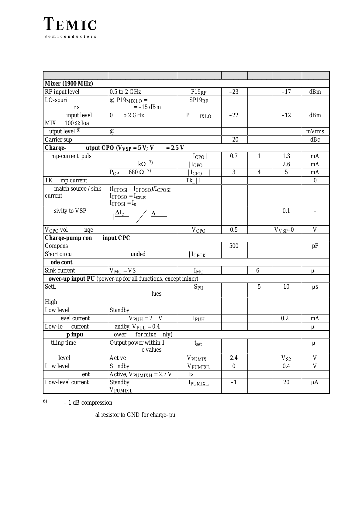
Electrical Characteristics (continued)
pp
Á
Á
Á
Á
Á
Á
Á
Á
Á
Á
Á
Á
Á
Á
Á
Á
Á
Á
Á
Á
Á
Á
Á
Á
T
= 25°C, VS = 2.7 to 5.5 V
amb
Parameters T est Conditions / Pin Symbol Min. T yp. Max. Unit
Mixer (1900 MHz)
RF input level
LO-spurious at
RF/NRF ports
MIXLO input level
MIXO (100 W load)
Output level
6)
Carrier suppression
Charge-pump output CPO (V
Pump-current pulse
TK pump current
Mismatch source / sink
ББББББ
current
ББББББ
Sensivity to VSP
ББББББ
V
voltage range
CPO
Charge-pump control input CPC
Compensation capacitor
Short circuit current
Mode control
Sink current
Power-up input PU (power-up for all functions, except mixer)
Settling time
High level
Low level
High-level current
Low-level current
Power-up input PUMIX (power -up for mixer only)
Settling time
High level
Low level
High-level current
Low-level current
ББББББ
6)
– 1 dB compression point (CP – 1)
0.5 to 2 GHz
@ P19
MIXLO
@ P19RF = –15 dBm
0.05 to 2 GHz
@ P19
MIXLO
@ P19
MIXLO
= 5 V; V
VSP
CPC open for DC
R
= 2.2 kΩ
CPC
P
= 680 Ω
CPC
(I
– I
CPOSI
ББББББ
I
CPOSO
I
ББББББ
CPOSI
D
|
8)
CPC grounded
CPOSO
= I
sourc
= I
sink
I
CPO
||
I
CPO
VMC = VS
Output power within 10%
of steady state values
Active
Standby
Active, V
Standby , V
PUH
PUL
Output power within 10%
of steady state values
Active
Standby
Active, V
PUMIXH
Standby ,
V
PUMIXL
ББББББ
= 0.4 V
= –10 dBm
= –17 dBm
= –17 dBm
= 2.5 V)
CPO
7)
7)
)/I
CPOSI
D
VSP
VSP
= 2.7 V
= 0.4 V
= 2.7 V
SP19
P19
P19
CS19
| I
| I
Tk_| I
ÁÁÁÁ
ÁÁÁÁ
|
ÁÁÁÁ
| I
V
V
I
I
ÁÁÁÁ
P19
RF
RF
MIXLO
MIXO
MIXO
| I
|
CPO
CPO 2
CPO_4
CPC
M
ICPO
S
ICPO
V
CPO
C
CPC
CPCK
I
MC
S
PU
V
PUH
V
PUL
I
PUH
I
PUL
t
setl
PUMIXH
PUMIXL
PUMIXH
PUMIXL
–23
–22
55
–20
0.7
|
|
|
1.4
3
ÁÁ
ÁÁ
ÁÁÁÁÁÁÁÁ
1
2
4
ÁÁ
ÁÁ
0.5
500
|
1.6
60
5
2.4
0
–1
5
2.4
0
–1
ÁÁ
ÁÁÁÁÁ
U2894B
–17
–40
–12
ÁÁ
ÁÁ
V
VSP
0.26
V
0.26
1.3
2.6
5
15
0.1
0.1
–0.6
10
0.4
20
10
S2
0.4
20
dBm
dBm
dBm
mVrms
dBc
mA
mA
mA
%/100°K
–
ÁÁ
ÁÁ
–
ÁÁ
V
pF
mA
m
A
m
s
V
V
mA
m
A
m
s
V
V
mA
m
A
ÁÁ
7)
8)
Rev . A4, 30-Sep-98 5 (16)
R
: external resistor to GND for charge–pump current control
CPC
See figure 7.
Page 6
U2894B
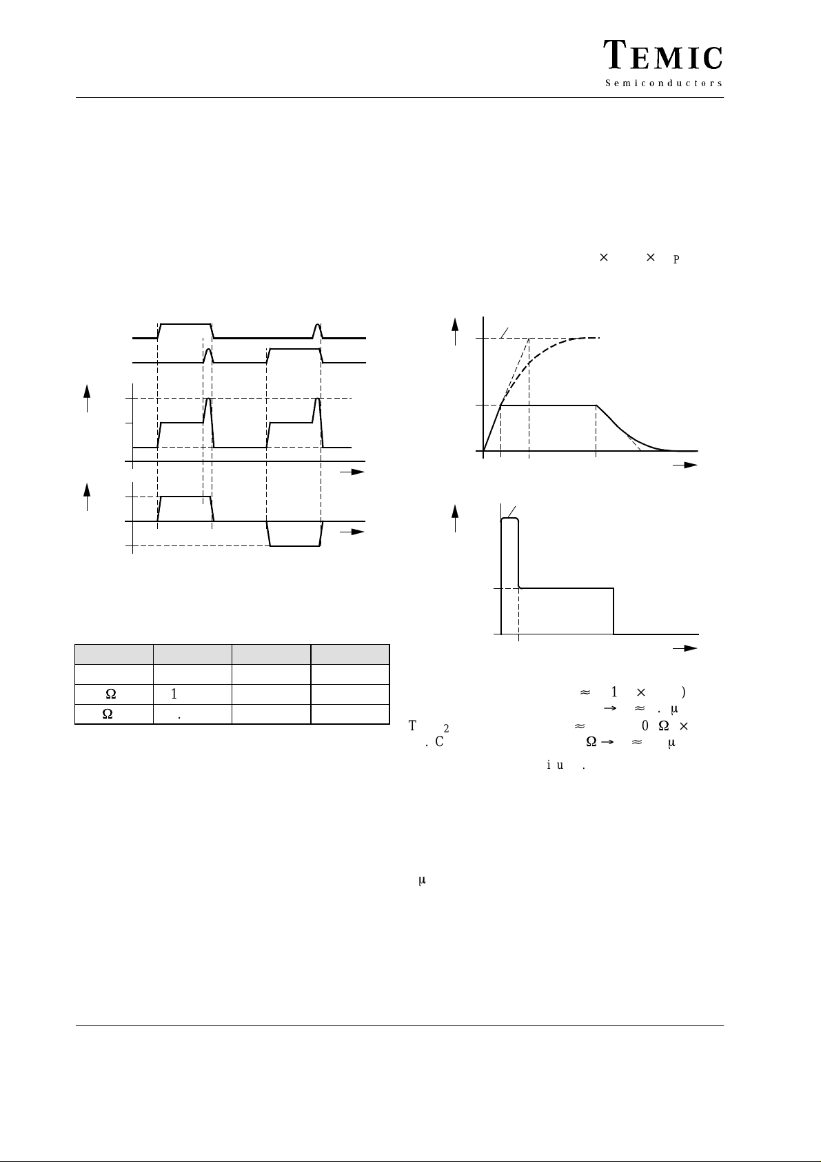
Supply Current of the Charge Pump
I
vs. Time
VSP
Due to the pulsed operation of the charge pump, the current into the charge-pump supply pin VSP is not constant.
Depending on I (see figure 6) and the phase difference at
the phase detector inputs, the current I
ries. Basically , the total current is the sum of the quiescent
current, the charge-/discharge current, and – after each
phase comparison cycle – a current spike (see figure 3).
Up
Down
5I
I
VSP
3I
I
2I
I
CPO
–2I
over time va-
VSP
t
t
14552
Initial Charge-Pump Current after
Power-Up
Due to stability reasons, the reference current generator
for the charge pump needs an external capacitor (>500 pF
from CPC to GND). After power-up, only the on-chip
generated current I = I
external capacitor. Due to the char ge pump’s architecture,
the charge pump current will be 2 I = 2 I
the voltage on CPC has reached the reference voltage
(1.1 V). The following figures illustrate this behavior .
I
CPCK
V
CPC
V
Ref
t
1
2x I
I
CPC
is available for charging the
CPCK
x R
CPC
t
0
CPCK
t
2
CPCK
t
until
Figure 3. Supply current of the charge pump = f(t)
Internal current, I, |I
R
CPC
| and I
CPC
I |I
CPC
vs. R
CPCO
CPC
| I
CPC open 0.5 mA 1 mA 0
2.2 k
680
W
W
1.0 mA 2 mA –0.5 mA
2.0 mA 4 mA –1.5 mA
(typical values)
CPC
I
t
1
Time t1 can be calculated as t1 [ (1.1 V C
e.g., C
Time t
e.g., C
The behavior of |I
= 1 nF, I
CPC
can be calculated as t2 [ (R
2
= 1 nF, R
CPC
= 2.7 mA ³ t1 [ 0.4 ms.
CPCK
= 2200 W ³ t2 [ 1.1 ms
CPC
Figure 4.
| after power-up can be very
CPO
/2200 W) C
CPC
t
CPC
14561
)/I
CPCK
CPC
advantageous for a fast settling of the loop. By using
larger capacitors (>1 nF), an even longer period with
maximum charge pump current is possible.
Ramp-up time for the internal band gap reference is about
1 ms. This time has to be added to the times calculated for
the charge pump reference.
Rev . A4, 30-Sep-986 (16)
Page 7
U2894B
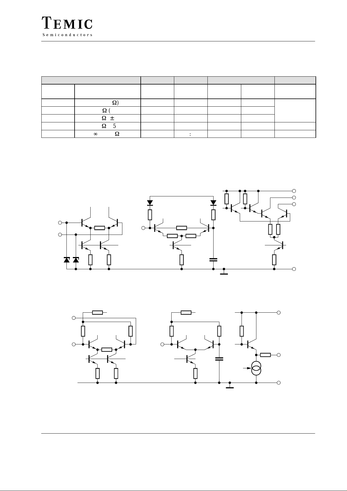
Mode Selection
The device can be programmed to different modes via an external resistor RMODE (including short, open) from Pin MC
to VS2. The mode is distinguished from specific N-, R-divider ratios, and the polarity of the charge pump current.
Mode Selection N-Divider R-Divider CPO Current Polarity
Mode Resistance between
fN < fR
1)
fN > fR
Pin MC and Pin VS2
1 0 (<50 W) 1:1 1:1 Sink Source
2 2.7 kW (±5%) 1:1 1:1 Source Sink
3 10 kW (±5%) 1:1 2:1 Source Sink
4 36 kW (±5%) 2:1 2:1 Source Sink PCN/PCS
5
1)
Frequencies referred to PFD input
2)
LO frequencies below VCO frequency
3)
LO frequencies above VCO frequency
4
) Sink current into Pin CPO. Source: current out from Pin CPO.
R
(>1 MW) 2:1 2:1 Sink Source GSM
Equivalent Circuits at the IC’s Pins
V
Bias_MDLO
2230 Ω2230 Ω
L,Q
MDLO
NI, NQ
250 Ω
4)
1)
Application
2)
3)
VS1
MDO
NMDO
V
Ref_input
Baseband input LO input Output
Figure 5. I/Q modulator
1 kΩ
RF
890 Ω 890 Ω
NRF
LO input
V
Bias_RF
V
MIXLO
Ref_RF
Figure 6. Mixer
V
Ref_MDLO
30 pF
1 kΩ
1.6 kΩ 1.6 kΩ
V
Ref_LO
Output
V
Bias_LO
40 pF
V
Ref_output
GND
14553
VS3
6.3 Ω
MIXO
GND
14554
Rev . A4, 30-Sep-98 7 (16)
Page 8
U2894B
VS2
CPC
GND
ND/RD
NND/NRD
4
I
I
/4
CPCK
V
Ref
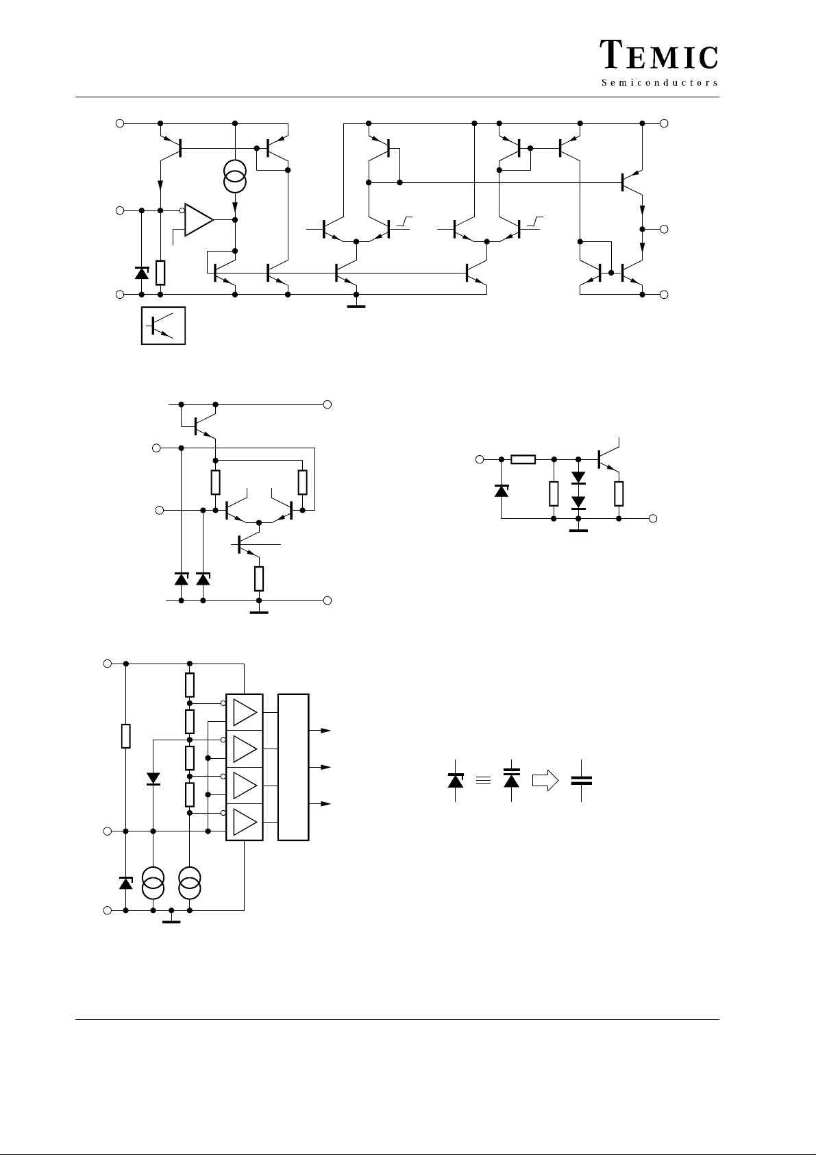
Figure 7. Charge pump
VS2
Ref_div
1.1 V
2230 Ω
= Transistor with an emitter area–factor of “n”
n
2 kΩ 2 kΩ
4
up
Ref
2
PU, PUMIX
2
down
20 kΩ
30 kΩ
Figure 9. Power-up
2I
2I
VSP
4
CPO
GNDP
14555
GND
14557
VS2
MC
GND
Figure 8. Dividers
2x
60 µA
Figure 10. Mode control
Logic
GND
14556
N–divider
R–divider
MUX
14898
≅
C (U)
2.5 pF @ 2 V
C (U) is a non-linear junction capacitance
14559
Figure 11. ESD-protection diodes
Rev . A4, 30-Sep-988 (16)
Page 9
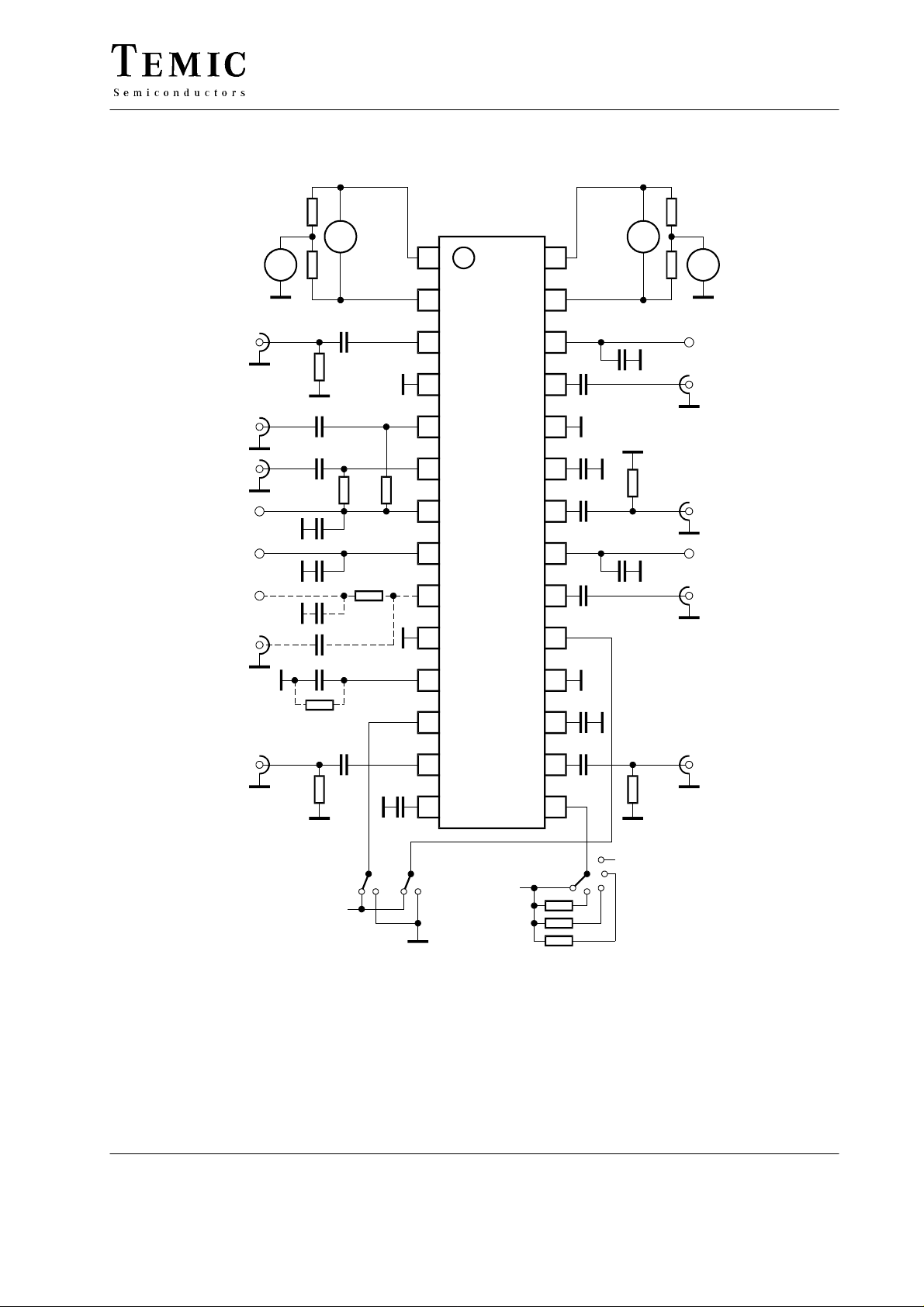
Test Circuit
U2894B
VDC
1.35 V –VS1/2 +0.1 V
Modulator
LO input
Modulator
outputs
V
S
VSP
VDO
Baseband input
VAC
50 Ω
<450 mV
50 Ω 50Ω
Baseband input
pp
<450 mV
281
2
27
pp
VAC
VDC
1.35 V –VS1/2 +0.1 V
3
4
5
6
26
25
24
23
V
S
Mixer
output
50 Ω
7
8
9
22
21
20
Mixer
input
V
S
Mixer
LO input
PFD
Pulse output
PFD
input
50 Ω
Bias voltage for
charge pump output:
0.5 V < VDO < VSP – 0.5 V
1 nF
V
10
11
12
13
19
18
17
16
PFD input
50 Ω
14
15
Mode control
Power–up
S
R
R
R
VS2
1
2
3
13315
Figure 12. Test circuit
Rev . A4, 30-Sep-98 9 (16)
Page 10
U2894B
Application Hints
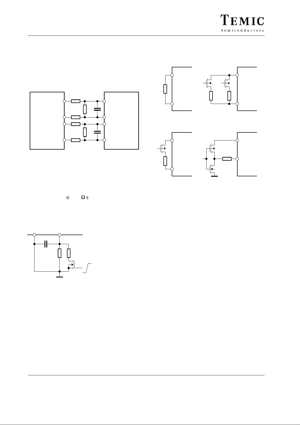
Interfacing
For some of the baseband ICs it may be necessary to
reduce the I/Q voltage swing so that it can be handled by
the U2894B. In those cases, the following circuitry can be
used.
R
II
Baseband IC
NI
Q
NQ
Figure 13. Interfacing the U2894B to I/Q baseband circuits
Due to a possible current offset in the differential baseband inputs of the U2894B the best values for the carrier
suppression of the I/Q modulator can be achieved with
voltage driven I/NI-, and Q/NQ-inputs. A value of
R
= R2/2*RS v 1.5 kW should be realized. RS is the
source
sum of R1 (above drawing) and the output resistance of
the baseband IC.
Charge-Pump Current Programming
1
R
R
R
2
1
1
R
2
NI
Q
U2894B
NQ
R
1
14562
Mode Control
U2894B
VS2
R
Mode
R
Mode1
MC
a) any single mode b) any 2 modes
U2894B
VS2
R
Mode
MC
c) any mode
& mode 5
Figure 15. Application examples for programming
different modes
R
Mode2
R
Mode
36 kΩor
10 kΩ
d) mode 5 & mode 3 or mode 4
U2894B
VS2
MC
U2894B
VS2
MC
14563
GND CPC
= 2.2 kΩ
R
CPC1
= 1 kΩ (incl. rds_on of FET)
R
R
CPC2
CPC2
‘H’
‘L’
|I
CPO
|I
CPO
| = 4 mA
| = 2 mA
1 nF
R
CPC1
Figure 14. Programming the charge-pump current
12497
Rev . A4, 30-Sep-9810 (16)
Page 11
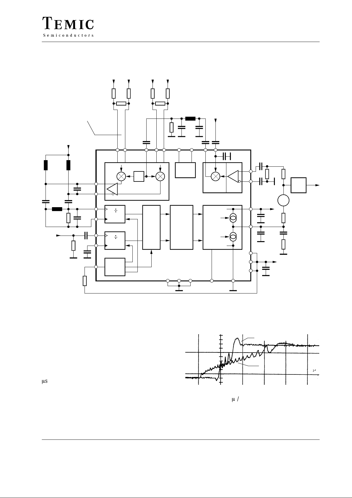
Application Circuit for DCS1800 (1710 – 1785 MHz)
Baseband processor
Attention!
Differential source impedance
seen by the I/NI, Q/NQ inputs
should not exceed 1000 Ohms
2.7 to 3.5 V
200 Ω
r_diff
15 nH
2x
15 pF
f_LO (–10 dBm)
1310–1385 MHz
25 2019122728321
U2894B
12 nH 12 nH
4.7 pF
2 pF2 pF
24 nH
820 Ω
f_Ref
V
= 55 mV
rms
(400 MHz)
4.7 pF
50 Ω
36 kΩ
Measurements
5
6
16
17
13
14
15
+
N1
divider
R1
divider
Mode
control
90°
I/Q modulator
MUX
Voltage
reference
PFD
Mixer
Charge
pump
101124184
22
23
to 3.5 V
8
9
7
21
26
Figure 16. Application circuit (power-up and charge-pump control is not shown)
2.7
68 pF
50 Ω
VCO
2.7 to 3.5 V
390 Ω
to PA
6 dB
attn.
f_TX
(1710–
1785 MHz)
MQE5A1–1747
3.3 nF
390 Ω
14570
Modulation-Loop Settling Time
CPC: 1 kΩ to GND
As valid for all PLL loops the settling time depends on
several factors. The following figure is an extraction from
measurements performed in an arrangement like the ap-
CPC ‘open’
plication circuit. It shows that a loop settling time of a few
m
s can be achieved.
Vertical: VCO tuning voltage 1 V/Div
Horizontal: Time 1 ms/Div
Figure 17.
Rev . A4, 30-Sep-98 11 (16)
Page 12
U2894B
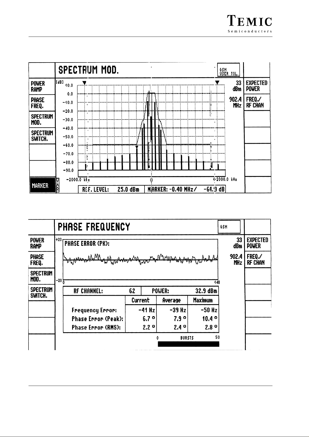
Modulation Spectrum & Phase Error
Application for GSM900
Figure 18. Modulation spectrum
Figure 19. Phase error
Rev . A4, 30-Sep-9812 (16)
Page 13
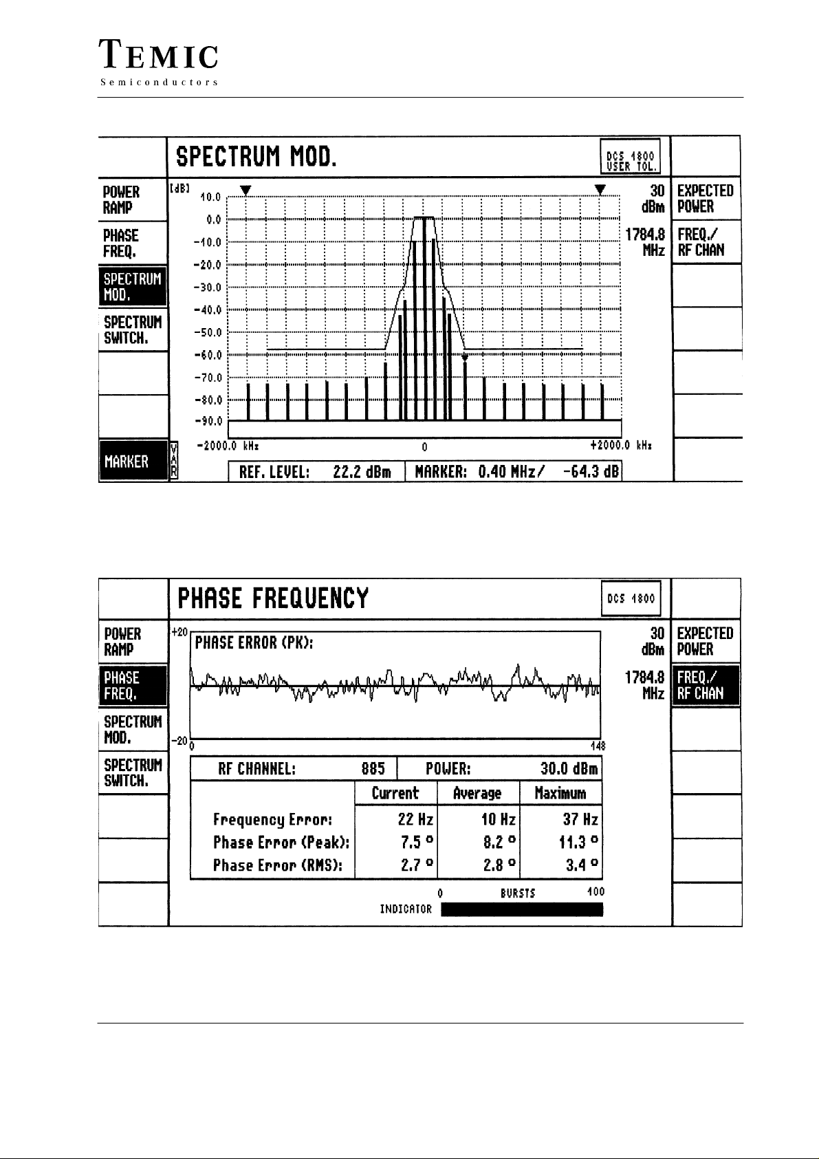
Application for DCS1800
U2894B
Figure 20. Modulation spectrum
Figure 21. Phase error
Rev . A4, 30-Sep-98 13 (16)
Page 14
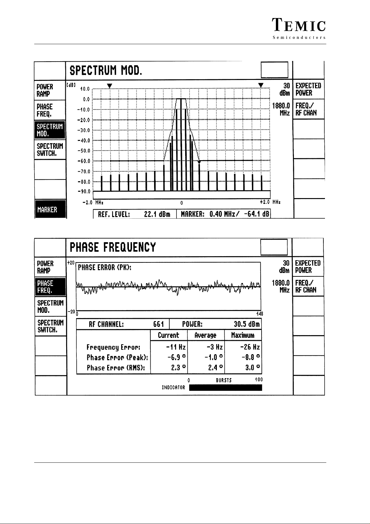
U2894B
Application for PCS1900
PCS 1900
USER TOL.
Figure 22. Modulation spectrum
Figure 23. Phase error
Complete transmitters (including PA) were measured.
The test equipment was the R & S CMD55 performing
standard approval tests. Typically, the spectrum @
400 kHz off the center carrier frequency is approximately
–65 dB attenuated (–60 dB according specificarion). The
PCS 1900
corresponding rms phase error is in the range of about 3°.
Dimensioning the loop-filters allows you to optimize
spectral-and phase error performance.
Rev . A4, 30-Sep-9814 (16)
Page 15
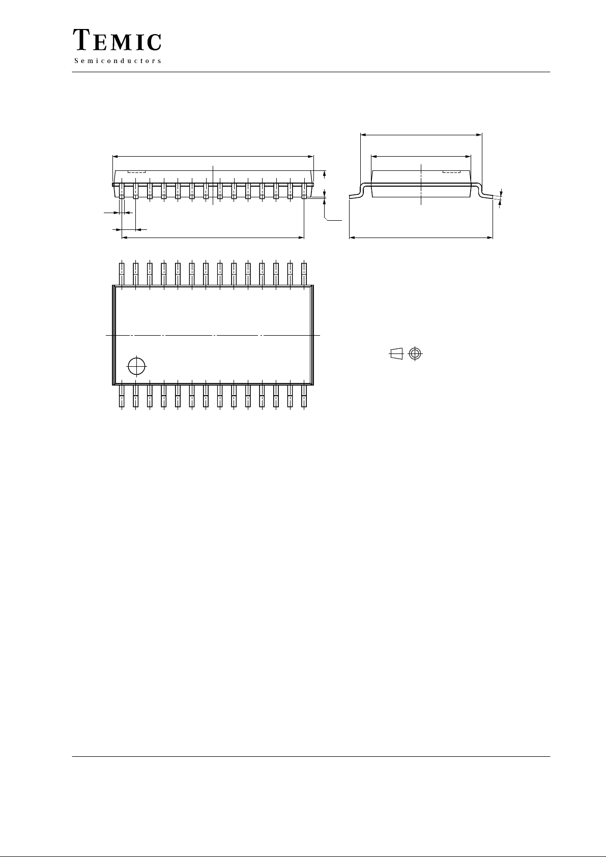
Package Information
U2894B
Package SSO28
Dimensions in mm
0.25
0.65
28 15
114
9.10
9.01
8.45
1.30
0.15
0.05
5.7
5.3
4.5
4.3
6.6
6.3
technical drawings
according to DIN
specifications
0.15
13018
Rev . A4, 30-Sep-98 15 (16)
Page 16

U2894B
Ozone Depleting Substances Policy Statement
It is the policy of TEMIC Semiconductor GmbH to
1. Meet all present and future national and international statutory requirements.
2. Regularly and continuously improve the performance of our products, processes, distribution and operating systems
with respect to their impact on the health and safety of our employees and the public, as well as their impact on
the environment.
It is particular concern to control or eliminate releases of those substances into the atmosphere which are known as
ozone depleting substances (ODSs).
The Montreal Protocol ( 1987) and its London Amendments (1990) intend to severely restrict the use of ODSs and
forbid their use within the next ten years. Various national and international initiatives are pressing for an earlier ban
on these substances.
TEMIC Semiconductor GmbH has been able to use its policy of continuous improvements to eliminate the use of
ODSs listed in the following documents.
1. Annex A, B and list of transitional substances of the Montreal Protocol and the London Amendments respectively
2. Class I and II ozone depleting substances in the Clean Air Act Amendments of 1990 by the Environmental
Protection Agency (EPA) in the USA
3. Council Decision 88/540/EEC and 91/690/EEC Annex A, B and C (transitional substances) respectively.
TEMIC Semiconductor GmbH can certify that our semiconductors are not manufactured with ozone depleting
substances and do not contain such substances.
We reserve the right to make changes to improve technical design and may do so without further notice.
Parameters can vary in different applications. All operating parameters must be validated for each customer
application by the customer. Should the buyer use TEMIC products for any unintended or unauthorized
application, the buyer shall indemnify TEMIC against all claims, costs, damages, and expenses, arising out of,
directly or indirectly, any claim of personal damage, injury or death associated with such unintended or
unauthorized use.
TEMIC Semiconductor GmbH, P.O.B. 3535, D-74025 Heilbronn, Germany
T elephone: 49 (0)7131 67 2594, Fax number: 49 (0)7131 67 2423
Rev . A4, 30-Sep-9816 (16)
 Loading...