

Datasheet U0406FC36C, U0406FC3.3C, U0406FC24C, U0406FC15C, U0406FC08C Datasheet (PROTEK)
...Page 1

05160
Only One Name Means ProTek’Tion™
APPLICATIONS
✔ Cellular Phones
✔ MCM Boards
✔ Wireless Communication Circuits
✔ IR LEDs
✔ SMART & PCMCIA Cards
IEC COMPATIBILITY (EN61000-4)
✔ 61000-4-2 (ESD): Air - 15kV, Contact - 8kV
✔ 61000-4-4 (EFT): 40A - 5/50ns
FEATURES
✔ ESD Protection > 25 kilovolts
✔ Available in Multiple Voltage Types Ranging From 3.3V to 36V
✔ 250 Watts Peak Pulse Power per Line (tp = 8/20µs)
✔ Bidirectional Configuration & Monolithic Structure
✔ Protects 3 to 5 Lines
U0406FC3.3C
thru
U0406FC36C
UNBUMPED FLIP CHIP ARRAY
MECHANICAL CHARACTERISTICS
✔ Standard EIA Chip Size: 0406
✔ Weight 0.73 milligrams (Approximate)
✔ Flammability Rating UL 94V-0
✔ 8mm Plastic & Paper Tape and Reel Per EIA Standard 481
✔ Device Marking On Reel
PIN CONFIGURATION
105160.R2 8/03 www.protekdevices.com
Page 2
DEVICE CHARACTERISTICS
MAXIMUM RATINGS @ 25°C Unless Otherwise Specified
U0406FC3.3C
thru
U0406FC36C
PARAMETER
Peak Pulse Power (tp = 8/20µs) - See Figure 1
Operating Temperature
Storage Temperature
SYMBOL VALUE
P
PP
T
J
T
STG
250 Watts
-55°C to 150°C
-55°C to 150°C°C
ELECTRICAL CHARACTERISTICS PER LINE @ 25°C Unless Otherwise Specified
PA RT
NUMBER
(See Note 1)
U0406FC3.3C
U0406FC05C
U0406FC08C
U0406FC12C
U0406FC15C
U0406FC24C
U0406FC36C
Note 1: All devices are bidirectional. Electrical characteristics apply in both directions.
Note 2: *Maximum leakage current < 5µA @ 2.8V. **Maximum leakage current <500nA @ 3.3V. ***Maximum leakage current <200nA @ 5V.
RATED
STAND-OFF
VOLTAGE
V
WM
VOLTS
3.3
5.0
8.0
12.0
15.0
24.0
36.0
MINIMUM
BREAKDOWN
VOLTAGE
@ 1mA
V
(BR)
VOLTS
4.0
6.0
8.5
13.3
16.7
26.7
40.0
MAXIMUM
CLAMPING
VOLTAGE
(See Fig. 2)
@ IP = 1A
V
C
VOLTS
7.0
9.8
13.4
19.0
24.0
43.0
64.0
MAXIMUM
CLAMPING
VOLTAGE
(See Fig. 2)
@8/20µs
VC @ I
PP
12.5V @ 20A
14.7V @ 17A
19.2V @ 13A
29.7V @ 9.0A
35.7V @ 7.0A
55.0V @ 5.0A
84.0V @ 3.0A
MAXIMUM
LEAKAGE
CURRENT
(See Note 2)
@V
WM
I
D
µA
75*
10**
10***
1
1
1
1
UNITS
°C
TYPICAL
CAPACITANCE
@0V, 1 MHz
C
pF
150
100
75
50
40
30
25
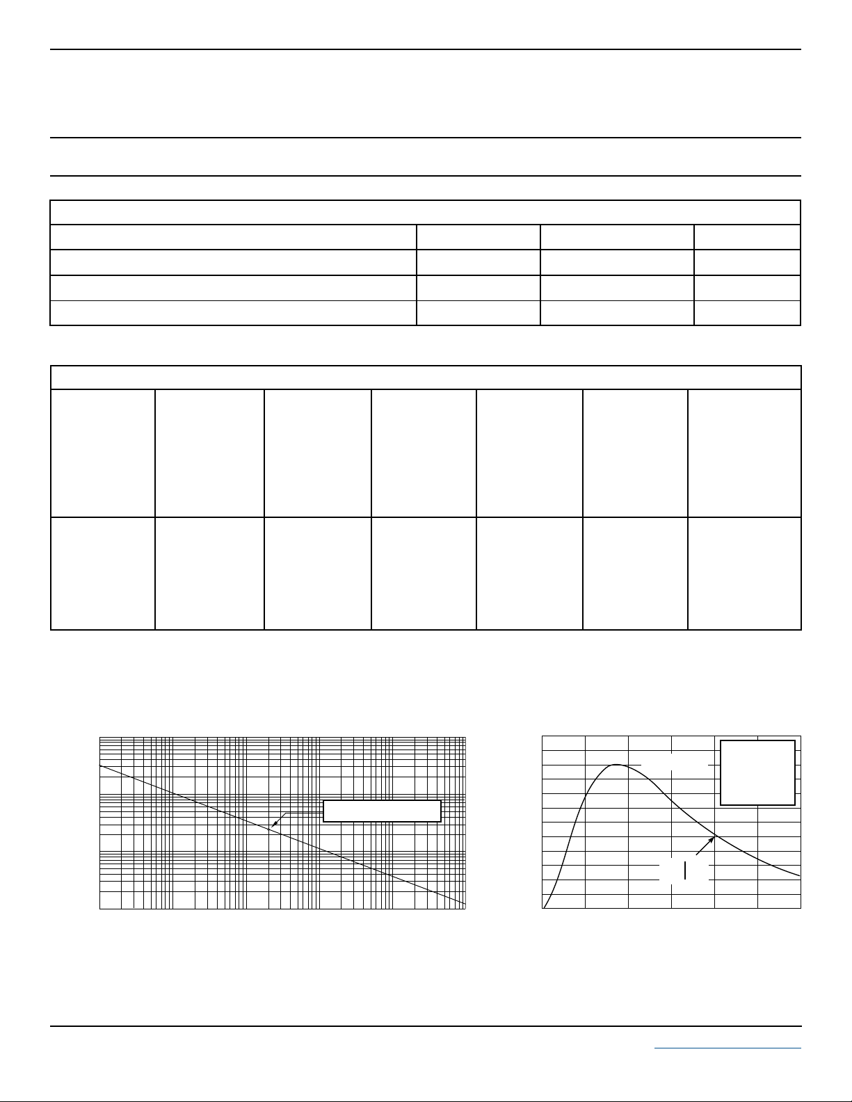
10,000
1,000
100
- Peak Pulse Current - Watts
PP
P
10
0.01 1 10 100 1,000 10,000
PEAK PULSE POWER VS PULSE TIME
FIGURE 1
t
- Pulse Duration - µs
d
250W, 8/20µs Waveform
FIGURE 2
120
PP
100
80
60
40
- Peak Pulse Current - % of I
20
PP
I
0
0 5 10 15 20 25 30
2 www.protekdevices.com05160.R2 8/03
PULSE WAVE FORM
t
f
Peak Value I
-t
e
td = t
t - Time - µs
PP
IPP/2
TEST
WAVEFORM
PARAMETERS
tf = 8µs
td = 20µs
Page 3
GRAPHS
U0406FC3.3C
thru
U0406FC36C
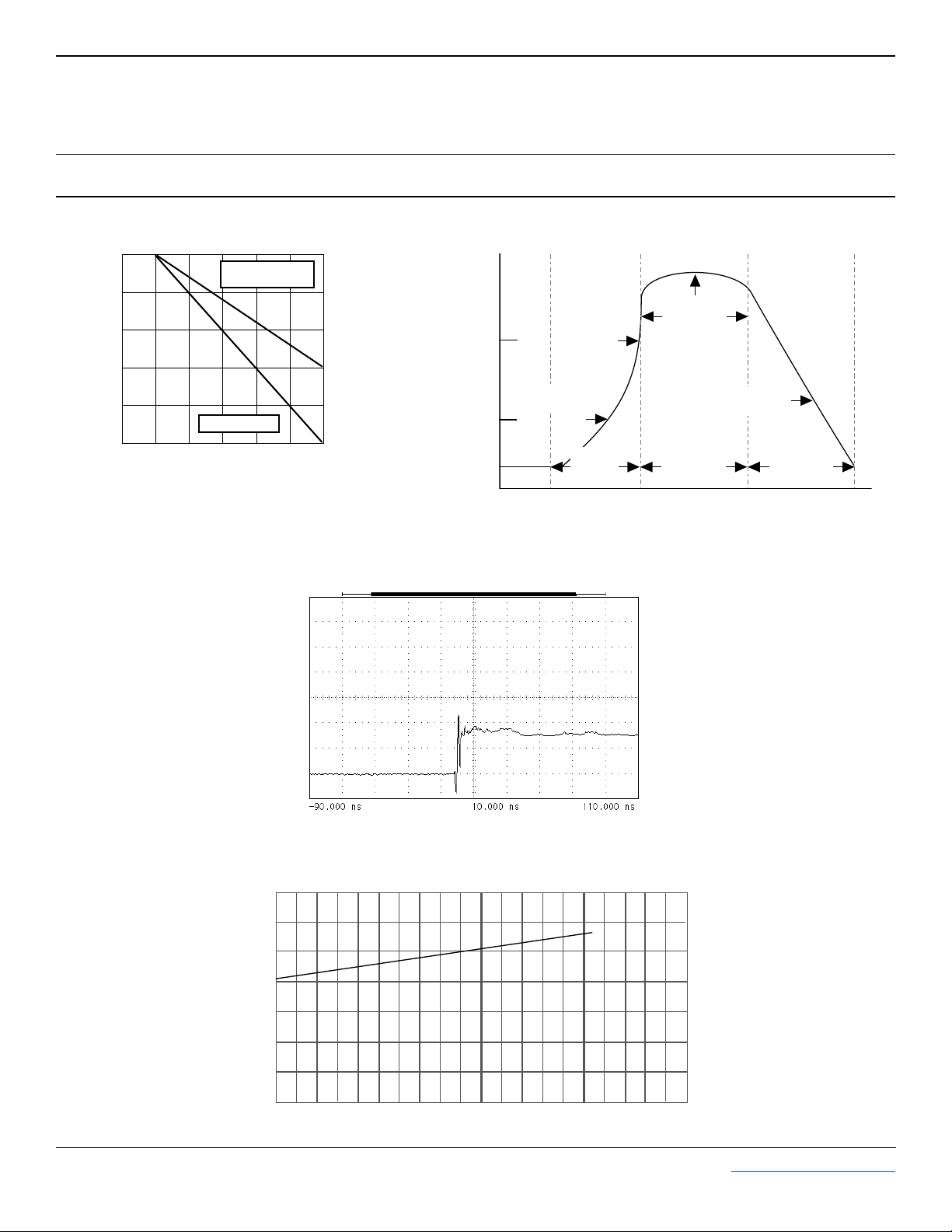
POWER DERATING CURVE
FIGURE 3
100
80
60
40
% Of Rated Power
20
0
0 25 50 75 100 125 150
TL - Lead Temperature - °C
Peak Pulse Power
8/20µs
Average Power
REFLOW SOLDER PROFILE
200°C
100°C
Note: This reflow profile does not take into account the printed circuit board (PCB) material
heating time. Additional time may be required for the preheat time and cool down time upon the
PCB or board material.
Instantaneous
to 200°C
1-2 Minutes
to 150°C
Pre-Heat
Time
FIGURE 5
OVERSHOOT & CLAMPING VOLTAGE FOR U0406FC05C
35
25
FIGURE 4
225°C
5-10 sec
1-2 Minutes to 25°C
Soldering
Time
Cool Down
Time
15
5 Volts per Division
5
-5
ESD Test Pulse - 25 kilovolt, 1/30ns (waveshape)
FIGURE 6
TYPICAL CLAMPING VOLTAGE VS PEAK PULSE CURRENT FOR U0406FC05C
14
12
10
8
6
4
- Clamping Voltage - Volts
C
V
2
0
0 5 10 15 20
- Peak Pulse Current - Amps
I
PP
3 www.protekdevices.com05160.R2 8/03
Page 4
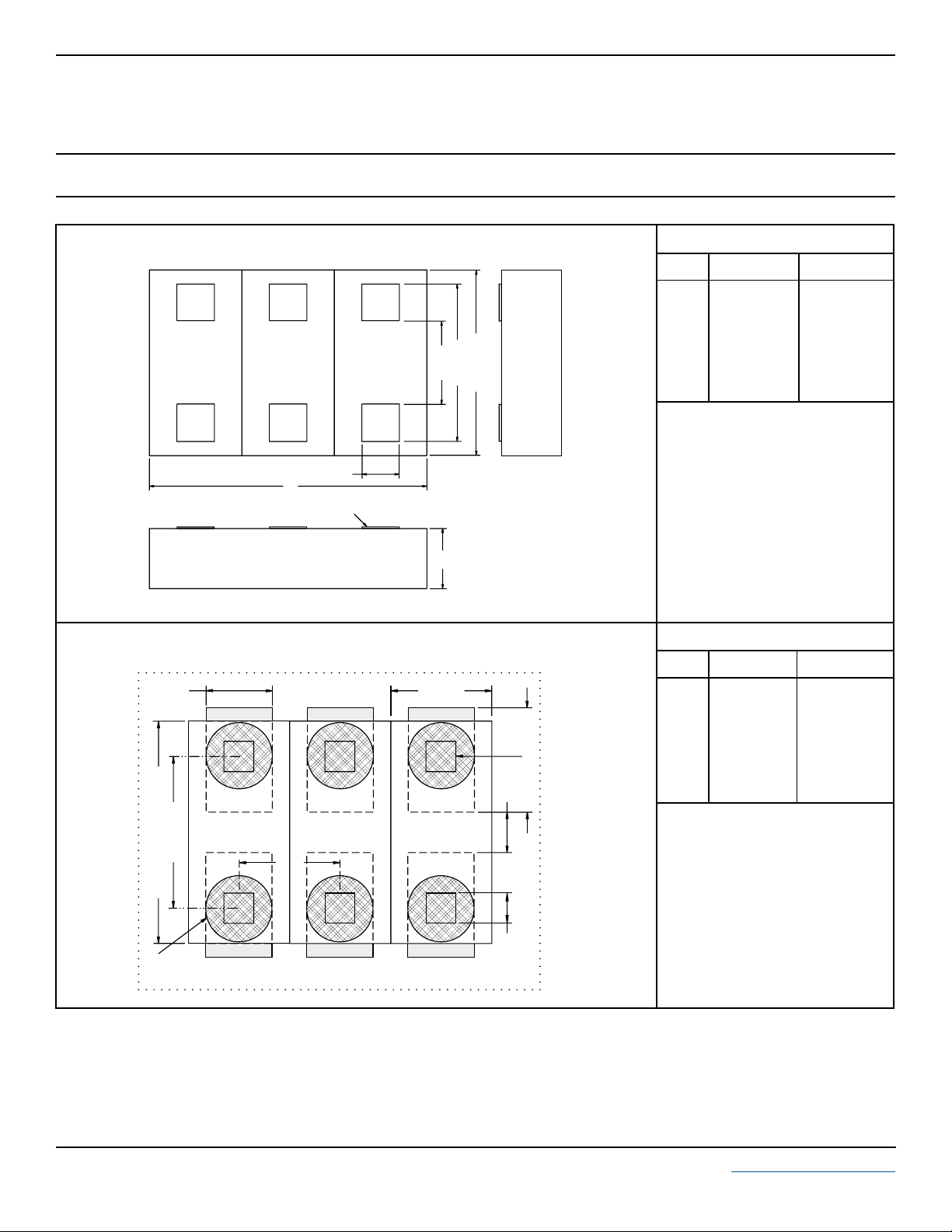
PACKAGE OUTLINE & DIMENSIONS
U0406FC3.3C
thru
U0406FC36C
PACKAGE OUTLINE
TOP
F
Metalized Die Contacts
END
E
MOUNTING PAD LAYOUT - Option 1
C
H
G
PACKAGE DIMENSIONS
MILLIMETERS
DIM
A
B
C
B
A
C
I
SIDE
E
F
I
NOTES:
1. Controlling dimensions in inches.
2. Decimal tolerances for mounting pad and
outline: .xxx ± 0.05mm (± 0.002”).
0.56 NOM
0.86 NOM
0.99 ± 0.0254
0.15 SQ
1.5 ± 0.0254
0.406 NOM
INCHES
0.022 NOM
0.034 NOM
0.039 ± 0.001
0.006 SQ
0.059 ± 0.001
0.016 NOM
PAD DIMENSIONS
MILLIMETERS
A
D
E
DIE
CONTACT
DIM
A
C
D
E
F
G
H
I
NOTE:
1.
Preferred:
0.51
0.30
0.46
0.20
0.15 SQ
0.71
0.99
0.51
Using 0.1mm (0.004”) stencil.
INCHES
0.020
0.012
0.018
0.008
0.006 SQ
0.028
0.039
0.020
SOLDER PRINT
0.010” - 0.012” DIA.
I
SOLDER PADS
F
SOLDER MASK
Outline & Dimensions: Rev 2 - 11/02, 06025
4 www.protekdevices.com05160.R2 8/03
Page 5
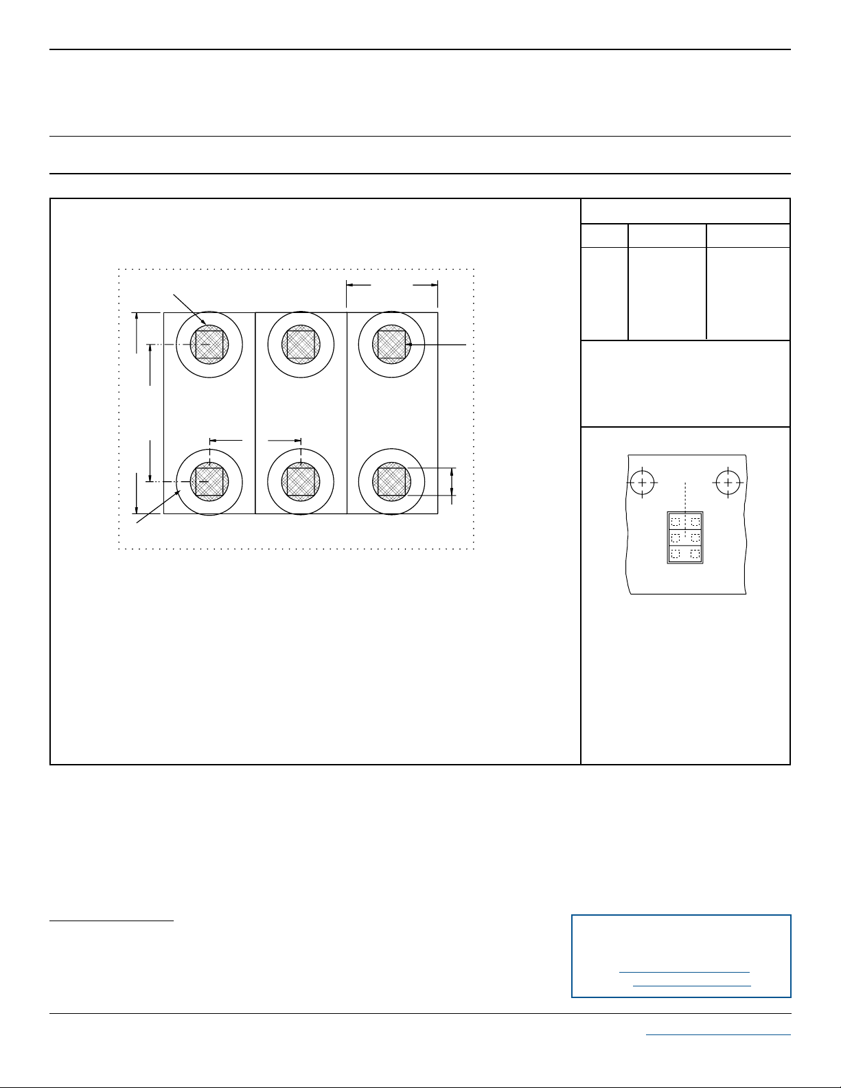
PACKAGE OUTLINE & DIMENSIONS
U0406FC3.3C
thru
U0406FC36C
MOUNTING PAD LAYOUT - Option 2
COPPER CONTACTS
0.009” [0.23] DIA.
H
G
SOLDER PRINT
0.014” [0.36] DIA.
PACKAGE DIMENSIONS
MILLIMETERS
DIM
A
A
DIE
SOLDER
CONTACT
I
F
SOLDER MASK
F
G
H
I
NOTES:
1. Controlling dimensions in inches.
2. Decimal tolerances for mounting pad and
outline: .xxx ± 0.05mm (± 0.002”).
3.
Preferred:
Outline & Dimensions: Rev 2 - 11/02, 06025
TAPE & REEL ORIENTATION
NOTE:
1. Top view of tape. Solder bumps are face
down in tape package.
0.51
0.15 SQ
0.71
0.99
0.51
Using 0.1mm (0.004”) stencil.
Triple Die - 0406
INCHES
0.020
0.006 SQ
0.028
0.039
0.020
COPYRIGHT © ProTek Devices 2003
SPECIFICATIONS: ProTek reserves the right to change the electrical and or mechanical
characteristics described herein without notice (except JEDEC).
DESIGN CHANGES: ProTek reser ves the right to discontinue product lines without notice, and that
the final judgement concerning selection and specifications is the buyer’s and that in furnishing
engineering and technical assistance, ProTek assumes no responsibility with respect to the
selection or specifications of such products.
TAPE & REEL ORDERING NOMENCLATURE
1. Surface mount product is taped and
reeled in accordance with EIA 481.
2.
8mm Plastic Tape:
pieces per reel. Ordering Suffix: -T75-1
(i.e., U0406FC05C-T75-1).
3.
8mm Paper Tape:
pieces per reel. Ordering Suffix: -T75-2
(i.e., U0406FC05C-T75-2).
7 Inch Reels - 5,000
7 Inch Reels - 5,000
ProTek Devices
2929 South Fair Lane, Tempe, AZ 85282
Tel: 602-431-8101 Fax: 602-431-2288
E-Mail: sales@protekdevices.com
Web Site: www.protekdevices.com
5 www.protekdevices.com05160.R2 8/03
 Loading...