

Page 1
Features
Planar Die Construction
·
500mW Power Dissipation on FR-4 PCB
·
General Purpose, Medium Current
·
TZX2V4 - TZX36C
500mW EPITAXIAL PLANAR ZENER DIODE
A
B
A
Mechanical Data
Case: DO-35, Glass
·
Leads: Solderable per MIL-STD-202,
·
PRELIMINARY
Method 208
Marking: Type Number
·
Polarity: Cathode Band
·
Weight: 0.35 grams (approx.)
·
Maximum Ratings
Characteristic Symbol Value Unit
Zener Current (See Table on page 2)
Forward Voltage @ IF= 200mA
Power Dissipation (Note 1)
Thermal Resistance, Junction to Ambient Air (Note 1)
Operating and Storage Temperature Range
Notes: 1. Valid provided that leads are kept at ambient temperature.
2. Tested with pulses, t £ 1.0ms.
@ TA= 25°C unless otherwise specified
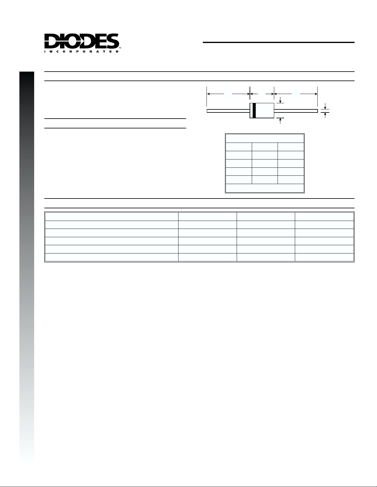
C
DO-35
Dim Min Max
A
B
C
D
All Dimensions in mm
¾¾¾
V
F
P
d
R
qJA
T
j,TSTG
25.40 ¾
¾ 4.00
¾ 0.60
¾ 2.00
1.5 V
500 mW
300 K/W
-65 to +175 °C
DS30089 Rev. 1P-5 1 of 4 TZX2V4 - TZX36C
Page 2

Electrical Characteristics
@ TA= 25°C unless otherwise specified
Type
Number
TZX2V4 2.3 2.6 5.0 100 5.0 0.5
TZX2V4A 2.3 2.5 5.0 100 5.0 0.5
TZX2V4B 2.4 2.6 5.0 100 5.0 0.5
PRELIMINARY
TZX2V7 2.5 2.9 5.0 100 5.0 0.5
TZX2V7A 2.5 2.7 5.0 100 5.0 0.5
TZX2V7B 2.6 2.8 5.0 100 5.0 0.5
TZX2V7C 2.7 2.9 5.0 100 5.0 0.5
TZX3V0 2.8 3.2 5.0 100 5.0 0.5
TZX3V0A 2.8 3.0 5.0 100 5.0 0.5
TZX3V0B 2.9 3.1 5.0 100 5.0 0.5
TZX3V0C 3.0 3.2 5.0 100 5.0 0.5
TZX3V3 3.1 3.5 5.0 100 5.0 1.0
TZX3V3A 3.1 3.3 5.0 100 5.0 1.0
TZX3V3B 3.2 3.4 5.0 100 5.0 1.0
TZX3V3C 3.3 3.5 5.0 100 5.0 1.0
TZX3V6 3.4 3.8 5.0 100 5.0 1.0
TZX3V6A 3.4 3.6 5.0 100 5.0 1.0
TZX3V6B 3.5 3.7 5.0 100 5.0 1.0
TZX3V6C 3.6 3.8 5.0 100 5.0 1.0
TZX3V9 3.7 4.1 5.0 100 5.0 1.0
TZX3V9A 3.7 3.9 5.0 100 5.0 1.0
TZX3V9B 3.8 4.0 5.0 100 5.0 1.0
TZX3V9C 3.9 4.1 5.0 100 5.0 1.0
TZX4V3 4.0 4.5 5.0 100 5.0 1.5
TZX4V3A 4.0 4.2 5.0 100 5.0 1.5
TZX4V3B 4.1 4.3 5.0 100 5.0 1.5
TZX4V3C 4.2 4.4 5.0 100 5.0 1.5
TZX4V3D 4.3 4.5 5.0 100 5.0 1.5
TZX4V7 4.4 4.9 5.0 100 5.0 2.0
TZX4V7A 4.4 4.6 5.0 100 5.0 2.0
TZX4V7B 4.5 4.7 5.0 100 5.0 2.0
TZX4V7C 4.6 4.8 5.0 100 5.0 2.0
TZX4V7D 4.7 4.9 5.0 100 5.0 2.0
TZX5V1 4.8 5.3 5.0 100 5.0 2.0
TZX5V1A 4.8 5.0 5.0 100 5.0 2.0
TZX5V1B 4.9 5.1 5.0 100 5.0 2.0
TZX5V1C 5.0 5.2 5.0 100 5.0 2.0
TZX5V1D 5.1 5.3 5.0 100 5.0 2.0
TZX5V6 5.2 5.9 5.0 40 5.0 2.0
TZX5V6A 5.2 5.5 5.0 40 5.0 2.0
TZX5V6B 5.3 5.6 5.0 40 5.0 2.0
TZX5V6C 5.4 5.7 5.0 40 5.0 2.0
TZX5V6D 5.5 5.8 5.0 40 5.0 2.0
TZX5V6E 5.6 5.9 5.0 40 5.0 2.0
Zener Voltage Range (Note 2) Test Current
VZ@I
ZT
Min (V) Max (V) mA
I
Maximum Zener
Impedance
ZT
Z
ZT @IZT
WmA
Maximum Reverse
Leakage Current
I
R
@V
V
R
Notes: 1. Valid provided that device terminals are kept at ambient temperature.
2. Tested with pulses, t £ 1.0ms.
DS30089 Rev. 1P-5 2 of 4 TZX2V4 - TZX36C
Page 3

Electrical Characteristics
@ TA= 25°C unless otherwise specified
Type
Number
TZX6V2 5.7 6.6 5.0 15 1.0 3.0
TZX6V2A 5.7 6.0 5.0 15 1.0 3.0
TZX6V2B 5.9 6.1 5.0 15 1.0 3.0
PRELIMINARY
TZX6V2C 6.0 6.3 5.0 15 1.0 3.0
TZX6V2D 6.1 6.4 5.0 15 1.0 3.0
TZX6V2E 6.3 6.6 5.0 15 1.0 3.0
TZX6V8 6.4 7.2 5.0 15 1.0 3.5
TZX6V8A 6.4 6.7 5.0 15 1.0 3.5
TZX6V8B 6.6 6.9 5.0 15 1.0 3.5
TZX6V8C 6.7 7.0 5.0 15 1.0 3.5
TZX6V8D 6.9 7.2 5.0 15 1.0 3.5
TZX7V5 7.0 7.9 5.0 15 1.0 5.0
TZX7V5A 7.0 7.3 5.0 15 1.0 5.0
TZX7V5B 7.2 7.6 5.0 15 1.0 5.0
TZX7V5C 7.3 7.7 5.0 15 1.0 5.0
TZX7V5D 7.5 7.9 5.0 15 1.0 5.0
TZX8V2 7.7 8.7 5.0 20 1.0 6.2
TZX8V2A 7.7 8.1 5.0 20 1.0 6.2
TZX8V2B 7.9 8.3 5.0 20 1.0 6.2
TZX8V2C 8.1 8.5 5.0 20 1.0 6.2
TZX8V2D 8.3 8.7 5.0 20 1.0 6.2
TZX9V1 8.5 9.7 5.0 20 1.0 6.8
TZX9V1A 8.5 8.9 5.0 20 1.0 6.8
TZX9V1B 8.7 9.1 5.0 20 1.0 6.8
TZX9V1C 8.9 9.3 5.0 20 1.0 6.8
TZX9V1D 9.1 9.5 5.0 20 1.0 6.8
TZX9V1E 9.3 9.7 5.0 20 1.0 6.8
TZX10 9.5 10.6 5.0 25 1.0 7.5
TZX10A 9.5 9.9 5.0 25 1.0 7.5
TZX10B 9.7 10.1 5.0 25 1.0 7.5
TZX10C 9.9 10.3 5.0 25 1.0 7.5
TZX10D 10.2 10.6 5.0 25 1.0 7.5
TZX11 10.4 11.6 5.0 25 1.0 8.2
TZX11A 10.4 10.8 5.0 25 1.0 8.2
TZX11B 10.7 11.1 5.0 25 1.0 8.2
TZX11C 10.9 11.3 5.0 25 1.0 8.2
TZX11D 11.1 11.6 5.0 25 1.0 8.2
TZX12 11.4 12.7 5.0 35 1.0 9.5
TZX12A 11.4 11.9 5.0 35 1.0 9.5
TZX12B 11.6 12.1 5.0 35 1.0 9.5
TZX12C 11.9 12.4 5.0 35 1.0 9.5
TZX12D 12.2 12.7 5.0 35 1.0 9.5
TZX13 12.4 13.4 5.0 35 1.0 10
TZX13A 12.4 12.9 5.0 35 1.0 10
TZX13B 12.6 13.1 5.0 35 1.0 10
TZX13C 12.9 13.4 5.0 35 1.0 10
Zener Voltage Range (Note 2) Test Current
VZ@I
ZT
Min (V) Max (V) mA
I
Maximum Zener
Impedance
ZT
Z
ZT @IZT
WmA
Maximum Reverse
Leakage Current
I
R
@V
V
R
Notes: 1. Valid provided that device terminals are kept at ambient temperature.
2. Tested with pulses, t £ 1.0ms.
DS30089 Rev. 1P-5 3 of 4 TZX2V4 - TZX36C
Page 4

Electrical Characteristics
@ TA= 25°C unless otherwise specified
Type
Number
TZX14 13.2 14.3 5.0 35 1.0 11
TZX14A 13.2 13.7 5.0 35 1.0 11
TZX14B 13.5 14.0 5.0 35 1.0 11
PRELIMINARY
TZX14C 13.8 14.3 5.0 35 1.0 11
TZX15 14.1 15.5 5.0 40 1.0 11.5
TZX15A 14.1 14.7 5.0 40 1.0 11.5
TZX15B 14.5 15.1 5.0 40 1.0 11.5
TZX15C 14.9 15.5 5.0 40 1.0 11.5
TZX16 15.3 17.1 5.0 45 1.0 12
TZX16A 15.3 15.9 5.0 45 1.0 12
TZX16B 15.7 16.5 5.0 45 1.0 12
TZX16C 16.3 17.1 5.0 45 1.0 12
TZX18 16.9 19.0 5.0 55 1.0 13
TZX18A 16.9 17.7 5.0 55 1.0 13
TZX18B 17.5 18.3 5.0 55 1.0 13
TZX18C 18.1 19.0 5.0 55 1.0 13
TZX20 18.8 21.2 2.0 60 1.0 15
TZX20A 18.8 19.7 2.0 60 1.0 15
TZX20B 19.5 20.4 2.0 60 1.0 15
TZX20C 20.2 21.2 2.0 60 1.0 15
TZX22 20.9 23.3 2.0 65 1.0 17
TZX22A 20.9 21.9 2.0 65 1.0 17
TZX22B 21.6 22.6 2.0 65 1.0 17
TZX22C 22.3 23.3 2.0 65 1.0 17
TZX24 22.9 25.5 2.0 70 1.0 19
TZX24A 22.9 24.0 2.0 70 1.0 19
TZX24B 23.6 24.7 2.0 70 1.0 19
TZX24C 24.3 25.5 2.0 70 1.0 19
TZX27 25.2 28.6 2.0 80 1.0 21
TZX27A 25.2 26.6 2.0 80 1.0 21
TZX27B 26.2 27.6 2.0 80 1.0 21
TZX27C 27.2 28.6 2.0 80 1.0 21
TZX30 28.2 31.6 2.0 100 1.0 23
TZX30A 28.2 29.6 2.0 100 1.0 23
TZX30B 29.2 30.6 2.0 100 1.0 23
TZX30C 30.2 31.6 2.0 100 1.0 23
TZX33 31.2 34.5 2.0 120 1.0 25
TZX33A 31.2 32.6 2.0 120 1.0 25
TZX33B 32.2 33.6 2.0 120 1.0 25
TZX33C 33.2 34.5 2.0 120 1.0 25
TZX36 34.2 38.0 2.0 140 1.0 27
TZX36A 34.2 35.7 2.0 140 1.0 27
TZX36B 35.3 36.8 2.0 140 1.0 27
TZX36C 26.4 38.0 2.0 140 1.0 27
Zener Voltage Range (Note 2) Test Current
VZ@I
ZT
Min (V) Max (V) mA
I
Maximum Zener
Impedance
ZT
Z
ZT @IZT
WmA
Maximum Reverse
Leakage Current
I
R
@V
V
R
Notes: 1. Valid provided that device terminals are kept at ambient temperature.
2. Tested with pulses, t £ 1.0ms.
DS30089 Rev. 1P-5 4 of 4 TZX2V4 - TZX36C
 Loading...