

Datasheet TXD2SS-L-9V-X, TXD2SS-L-9V, TXD2SS-L-6V-Z, TXD2SS-L-6V-X, TXD2SS-L-6V Datasheet (NAIS)
...Page 1
160
TX-D
RELAYS
HIGH INSULATION RELAYS
(Conforming to the supplementary
insulation class of EN Standards
(EN41003))
TESTING
8.2
.323
7.4
.291
15
.591
mm inch
8.4
.333
7.4
.291
15
.591
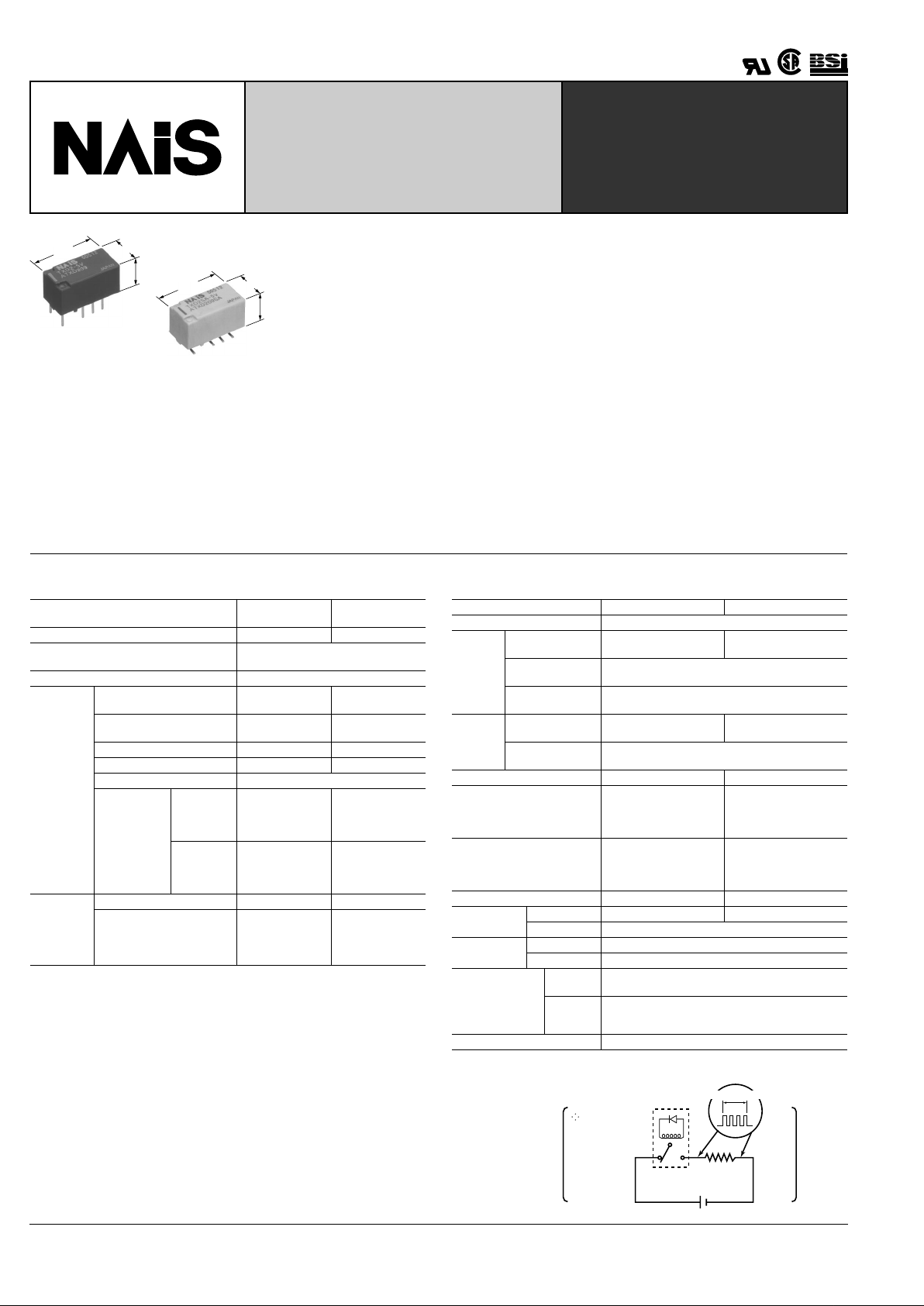
FEATURES
• Approved to the supplementary insulation class in the EN standards
(EN41003).
The insulation distance between the contact and coil meet the supplementary insulation class of the EN41003 standards
as required for equipment connected to
the telephone lines in Europe.
Satisfies the following conditions:
• Clearances: 2.0 mm .079 inch or more
• Creepage distance: 2.5 mm .098 inch or
more
• 2,000 V breakdown voltage between
contact and coil.
The body block construction of the coil
that is molded by plastic offers a high
breakdown voltage of 2,000 V between
contact and coil, and 1,000 V between
open contacts.
• Outstanding surge resistance.
Surge withstand between open contacts:
1,500 V 10 × 160 µ sec. (FCC part 68)
Surge withstand between contact and
coil: 2,500 V 2 × 10 µ sec. (Bellcore)
• High sensitivity 200 mW.
• High contact capacity: 2 A 30 V DC
(Standard type)
• Surface-mount type also available.
• M.B.B. type also available
• The use of gold-clad twin crossbar
contacts ensures high contact reliability.
• Outstanding vibration and shock resistance.
Functional shock resistance:
750 m/s
2
{75G}
Destructive shock resistance:
1,000 m/s
2
{100G}
Functional vibration resistance:
10 to 55 Hz (at double amplitude of 3.3
mm .130 inch)
Destructive vibration resistance:
10 to 55 Hz (at double amplitude of 5 mm
.197 inch)
• Sealed construction allows automatic
washing.
SPECIFICATIONS
Contact
Notes:
❇
1This value can change due to the switching frequency, en vironmental conditions,
and desired reliability level, therefore it is recommended to chec k this with the actual load.
❇
2The upper limit for the ambient temperature is the maximum temperature that
can satisfy the coil temperature rise. Under the packing condition, allo wable temperature range is from –40 to +70°C –40°C to +158°F.
Characteristics
Standard (B.B.M)
type
M.B.B.type
Arrangement 2 Form C 2 Form D
Initial contact resistance, max.
(By voltage drop 6 V DC 1 A)
100 m Ω
Contact material Gold-clad silver
Rating
Nominal switching
capacity (resistive load)
2 A 30 V DC 1 A 30 V DC
Max. switching power
(resistive load)
60 W 30 W
Max. switching voltage 220 V DC 110 V DC
Max. switching current 2 A 1 A
Min. switching capacity ❇ 1 10 µ A 10 mV DC
Nominal operating power
Single side
stable
200 mW
(1.5 to 12 V DC)
230 mW
(24 V DC)
250 mW
(1.5 to 12 V DC)
270 mW
(24 V DC)
1 coil
latching
150 mW
(1.5 to 12 V DC)
170 mW
(24 V DC)
—
Expected
life (min.
operations)
Mechanical (at 180 cpm) 10
8
10
7
Electrical (at 20 cpm)
10
5
(2 A 30 V DC
resistive),
5 ×
10
5
(1 A 30 V
DC resistive)
10
5
(1 A 30 V DC
resistive)
Standard (B.B.M) type M.B.B.type
Initial insulation resistance*
1
Min. 1,000 M Ω (at 500 V DC)
Initial
breakdown
voltage*
2
Between open
contacts
1,000 Vrms for 1 min. 500 Vrms for 1 min.
Between contact
and coil
2,000 Vrms for 1 min.
Between contact
sets
1,000 Vrms for 1 min.
Initial
surge
voltage
Between contacts, 10 × 160 µ s
1,500 V
[FCC Part 68]
–
Between contact
and coil, 2 × 10 µ s
2,500 V [Bellcore]
Temperature rise (at 20 ° C) Max. 50 ° C*
3
Max. 50 ° C*
4
Operate time [Set time]*
5
(at 20 ° C)
Max. 4 ms
(Approx. 2 ms)
[Max. 4 ms
(Approx. 2 ms)]
Max. 4 ms
(Approx. 2 ms)
Release time [Reset time]*
6
(at 20 ° C)
Max. 4 ms
(Approx. 1 ms)
[Max. 4 ms
(Approx. 2 ms)]
Max. 4 ms
(Approx. 1 ms)
M.B.B. time*
12
— Min. 10 µ s
Shock
resistance
Functional Min. 750 m/s
2
{75 G}*
7
Min. 500 m/s
2
{50 G}*
8
Destructive*
9
Min. 1,000 m/s
2
{100 G}
Vibration
resistance
Functional*
10
10 to 55 Hz at double amplitude of 3.3 mm
Destructive 10 to 55 Hz at double amplitude of 5 mm
Conditions for operation, transport and
storage*
11
(Not freezing and condensing
at low temperature)
Ambient
temp. ❇ 2
–40 ° C to +85 ° C –40 ° F to +185 ° F
Humidity 5 to 85%R.H.
Unit weight Approx. 2 g .071 oz.
Remarks
* Specifications will vary with foreign standards certification ratings.
*
1
Measurement at same location as "Initial breakdown voltage" section.
*
2
Detection current: 10 mA
*
3
By resistive method; nominal voltage applied to the coil; contact carrying current: 2 A.
*
4
By resistive method; nominal voltage applied to the coil; contact carrying current: 1 A.
*
5
Nominal voltage applied to the coil, excluding contact bounce time.
*
6
Nominal voltage applied to the coil, excluding contact bounce time without diode.
*
7
Half-wave pulse of sine wave: 6 ms.; detection time: 10 µ s.
*
8
Half-wave pulse of sine wave: 11 ms.; detection time: 10 µ s.
*
9
Half-wave pulse of sine wave: 6 ms.
*
10
Detection time: 10 µ s.
*
11
Refer to 4. Conditions f or operation, transport and storage mentioned in Cautions
for use (Page 178).
*
12
M.B.B. time:
Min. 10 µs
5 V DC
500 Ω
Measuring
condition
×
Page 2
TX-D
161
TYPICAL APPLICATIONS
• Facsimiles
• Modems
• Communication devices
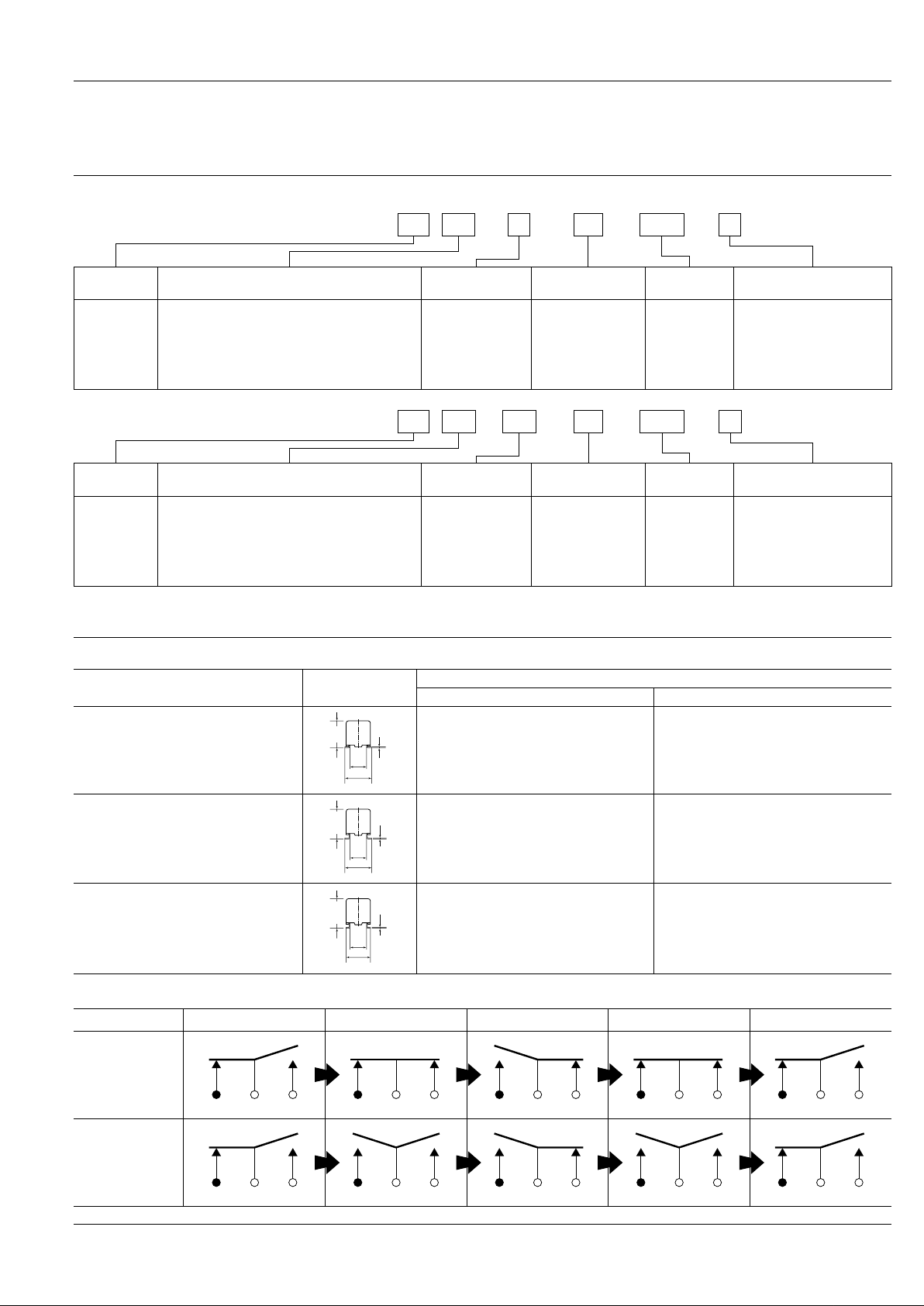
ORDERING INFORMATION
1) Standard (B.B.M.)type
2) M.B.B.type
Ex. TXD 2 SA L 4.5V Z–– – –
Contact
arrangement
Surface-mount availability Operating function Terminal shape
Coil voltage
(DC)
Packing style
2: 2 Form C Nil:
SA:
SL:
SS:
Standard PC board terminal or
self-clinching terminal
Standard surface-mount terminal
High connection reliability surface-mount
terminal type
Space saving surface-mount terminal type
Nil:L:Single side
stable
1 coil latching
Nil:H:Standard PC
board terminal
or surfacemount type
Self-clinching
terminal
1.5, 3, 4.5, 5,
6, 9, 12, 24 V
Nil:Z:Tube packing
Tape and reel packing
(Picked from the 8/9/
10/12-pin side)
Ex. TXD 2 SA 2M 4.5V Z–– – –
Contact
arrangement
Surface-mount availability Operating function Terminal shape
Coil voltage
(DC)
Packing style
2: 2 Form D Nil:
SA:
SL:
SS:
Standard PC board terminal or
self-clinching terminal
Standard surface-mount terminal
High connection reliability surface-mount
terminal type
Space saving surface-mount terminal type
2M: 2 M.B.B. type Nil:H:Standard PC
board terminal
or surfacemount type
Self- clinching
terminal
1.5, 3, 4.5, 5,
6, 9, 12, 24 V
Nil:Z:Tube packing
Tape and reel packing
(Picked from the 8/9/
10/12-pin side)
Notes: 1. Tape and reel (picked from 1/3/4/5-pin side) is also available by request. Part number. suffix “-X” is needed when ordering.
(ex.) TXD2SA-3V-X
2. Tape and reel packing symbol “-Z” or “-X” are not marked on the relay.
Surface-mount terminal variation
OPERATION INFORMATION
Variation Terminal style
Usable conditions based on terminal connection solder reliability
Normal environments (indoor) Drastic temperature fluctuations (outdoor)
SA type
(Standard surface-mount terminal type)
Recommended —
SL type
(Highly connection reliability surfacemount terminal type)
Recommended Recommended
SS type
(Space saving surface-mount terminal
type)
Recommended Recommended
5.08
.200
8.4
.331
0.25
.010
9.4
±0.5
.370
±.020
5.08
.200
Max.
10.0
.394
0.25
.010
9.4
±0.5
.370
±.020
5.08
.200
Max.
10.0
.394
0.25
.010
7.4
±0.5
.291
±.020
N.C. COM N.O.
N.C. COM N.O.
N.C. COM N.O.
N.C. COM N.O.
N.C. COM N.O.
N.C. COM N.O.
N.C. COM N.O.
N.C. COM N.O.
N.C. COM N.O.
N.C. COM N.O.
Contact Operation
M.B.B. contact
operation
Standard
(B.B.M.) contact
operation
Open During Operation Operation Complete During Reset Reset Complete
Page 3
TX-D
162
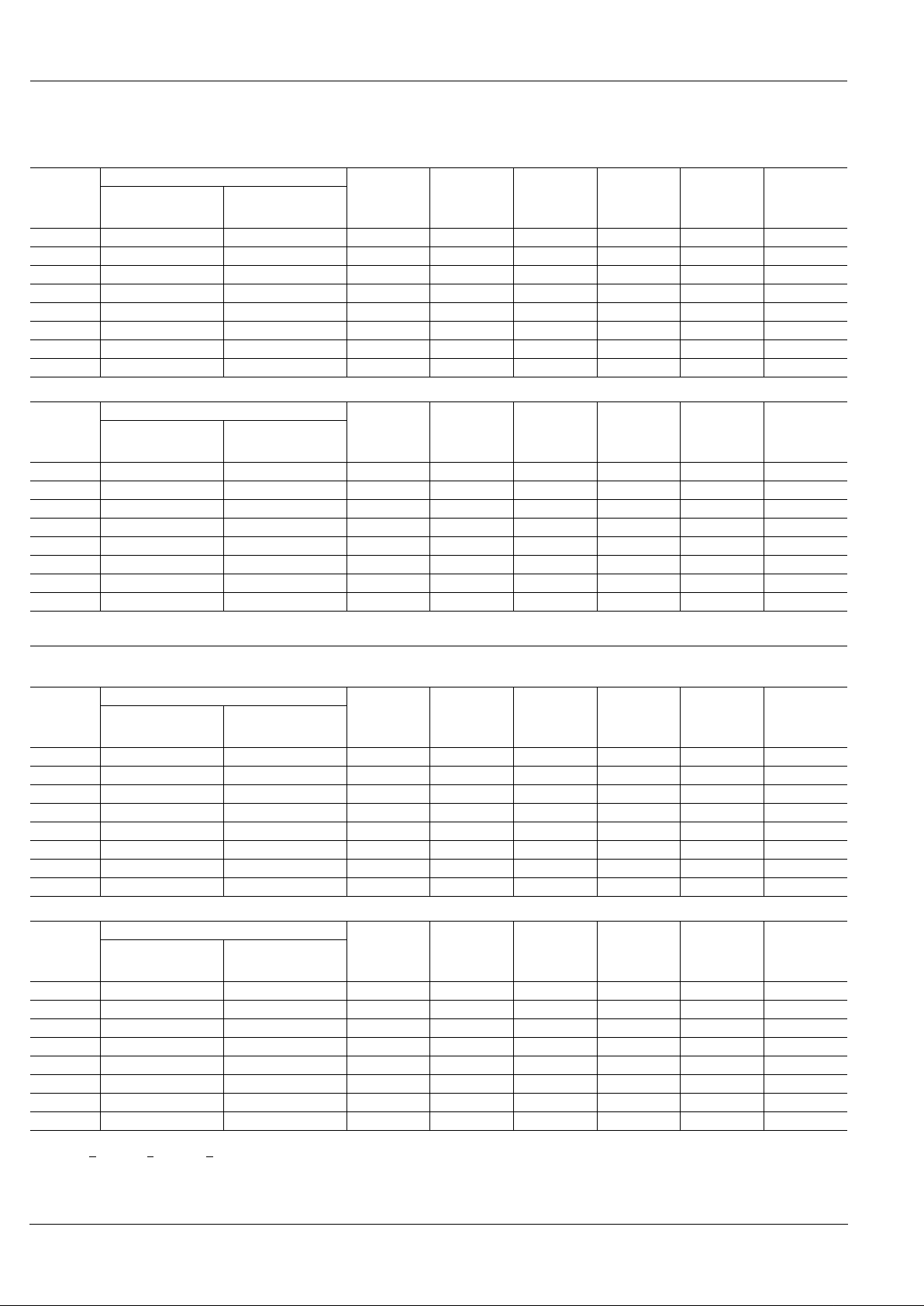
TYPES AND COIL DATA (at 20 ° C 68 ° F)
1. Standard (B.B.M.) type
(1) Standard PC board terminal and self-clinching terminal
1. Single side stable
2. 1 coil latching
Standard packing: 40 pcs. in an inner package (tube); 1,000 pcs. in an outer package.
Note: In case of 5 V transistor drive circuit, it is recommended to use 4.5 V type relay.
Coil
Rating,
V DC
Part No. V DC Pick-up
voltage,
V DC (max.)
(initial)
Drop-out
voltage,
V DC (min.)
(initial)
Nominal
operating
current,
mA ( ± 10%)
Coil
resistance,
Ω ( ±
10%)
Nominal
operating
power,
mW
Max.
allowable
voltage,
V DC
Standard PC board
terminal
Self-clinching
terminal
1.5 TXD2-1.5V TXD2-H-1.5V 1.13 0.15 132.7 11 200 1.8
3 TXD2-3V TXD2-H-3V 2.25 0.3 66.7 45 200 3.6
4.5 TXD2-4.5V TXD2-H-4.5V 3.38 0.45 44.4 101 200 5.4
5 TXD2-5V TXD2-H-5V 3.75 0.5 40.0 125 200 6
6 TXD2-6V TXD2-H-6V 4.5 0.6 33.3 180 200 7.2
9 TXD2-9V TXD2-H-9V 6.75 0.9 22.2 405 200 10.8
12 TXD2-12V TXD2-H-12V 9 1.2 16.7 720 200 14.4
24 TXD2-24V TXD2-H-24V 18 2.4 9.6 2,504 230 28.8
Coil
Rating,
V DC
Part No.
Set voltage,
V DC (max.)
(initial)
Reset
voltage,
V DC (max.)
(initial)
Nominal
operating
current,
mA ( ± 10%)
Coil
resistance,
Ω ( ±
10%)
Nominal
operating
power,
mW
Max.
allowable
voltage,
V DC
Standard PC board
terminal
Self-clinching
terminal
1.5 TXD2-L-1.5V TXD2-L-H-1.5V 1.13 1.13 100.0 15 150 1.8
3 TXD2-L-3V TXD2-L-H-3V 2.25 2.25 50.0 60 150 3.6
4.5 TXD2-L-4.5V TXD2-L-H-4.5V 3.38 3.38 33.3 135 150 5.4
5 TXD2-L-5V TXD2-L-H-5V 3.75 3.75 30.0 166 150 6
6 TXD2-L-6V TXD2-L-H-6V 4.5 4.5 25.0 240 150 7.2
9 TXD2-L-9V TXD2-L-H-9V 6.75 6.75 16.7 540 150 10.8
12 TXD2-L-12V TXD2-L-H-12V 9 9 12.5 960 150 14.4
24 TXD2-L-24V TXD2-L-H-24V 18 18 7.1 3,388 170 28.8
(2) Surface-mount terminal
1. Single side stable
2. 1 coil latching
❍
: For each surface-mounted terminal variation, input the following letter.
SA type: A
, SL type: L , SS type: S
Standard packing:40 pcs. (tube), 500 pcs. (tape and reel) in an inner package; 1,000 pcs. in an outer package
Notes:
1. Tape and reel packing symbol "-Z" is not marked on the relay. "X" type tape and reel packing (picked from 1/3/4/5-pin side) is also available.
2. In case of 5 V transistor drive circuit, it is recommended to use 4.5 V type relay.
Coil
Rating,
V DC
Part No. Pick-up
voltage,
V DC (max.)
(initial)
Drop-out
voltage,
V DC (min.)
(initial)
Nominal
operating
current,
mA ( ± 10%)
Coil
resistance,
Ω ( ±
10%)
Nominal
operating
power,
mW
Max.
allowable
voltage,
V DC
Tube packing
Tape and reel
packing
1.5 TXD2S ❍ -1.5V TXD2S ❍ -1.5V-Z 1.13 0.15 132.7 11 200 1.8
3 TXD2S ❍ -3V TXD2S ❍ -3V-Z 2.25 0.3 66.7 45 200 3.6
4.5 TXD2S ❍ -4.5V TXD2S ❍ -4.5V-Z 3.38 0.45 44.4 101 200 5.4
5 TXD2S ❍ -5V TXD2S ❍ -5V-Z 3.75 0.5 40.0 125 200 6
6 TXD2S ❍ -6V TXD2S ❍ -6V-Z 4.5 0.6 33.3 180 200 7.2
9 TXD2S ❍ -9V TXD2S ❍ -9V-Z 6.75 0.9 22.2 405 200 10.8
12 TXD2S ❍ -12V TXD2S ❍ -12V-Z 9 1.2 16.7 720 200 14.4
24 TXD2S ❍ -24V TXD2S ❍ -24V-Z 18 2.4 9.6 2,504 230 28.8
Coil
Rating,
V DC
Part No.
Set voltage,
V DC (max.)
(initial)
Reset
voltage,
V DC (max.)
(initial)
Nominal
operating
current,
mA ( ± 10%)
Coil
resistance,
Ω ( ±
10%)
Nominal
operating
power,
mW
Max.
allowable
voltage,
V DC
Tube packing
Tape and reel
packing
1.5 TXD2S ❍ -L-1.5V TXD2S ❍ -L-1.5V-Z 1.13 1.13 100.0 15 150 1.8
3 TXD2S ❍ -L-3V TXD2S ❍ -L-3V-Z 2.25 2.25 50.0 60 150 3.6
4.5 TXD2S ❍ -L-4.5V TXD2S ❍ -L-4.5V-Z 3.38 3.38 33.3 135 150 5.4
5 TXD2S ❍ -L-5V TXD2S ❍ -L-5V-Z 3.75 3.75 30.0 166 150 6
6 TXD2S ❍-L-6V TXD2S❍-L-6V-Z 4.5 4.5 25.0 240 150 7.2
9 TXD2S❍-L-9V TXD2S❍-L-9V-Z 6.75 6.75 16.7 540 150 10.8
12 TXD2S❍-L-12V TXD2S❍-L-12V-Z 9 9 12.5 960 150 14.4
24 TXD2S❍-L-24V TXD2S❍-L-24V-Z 18 18 7.1 3,388 170 28.8
Page 4
TX-D
163
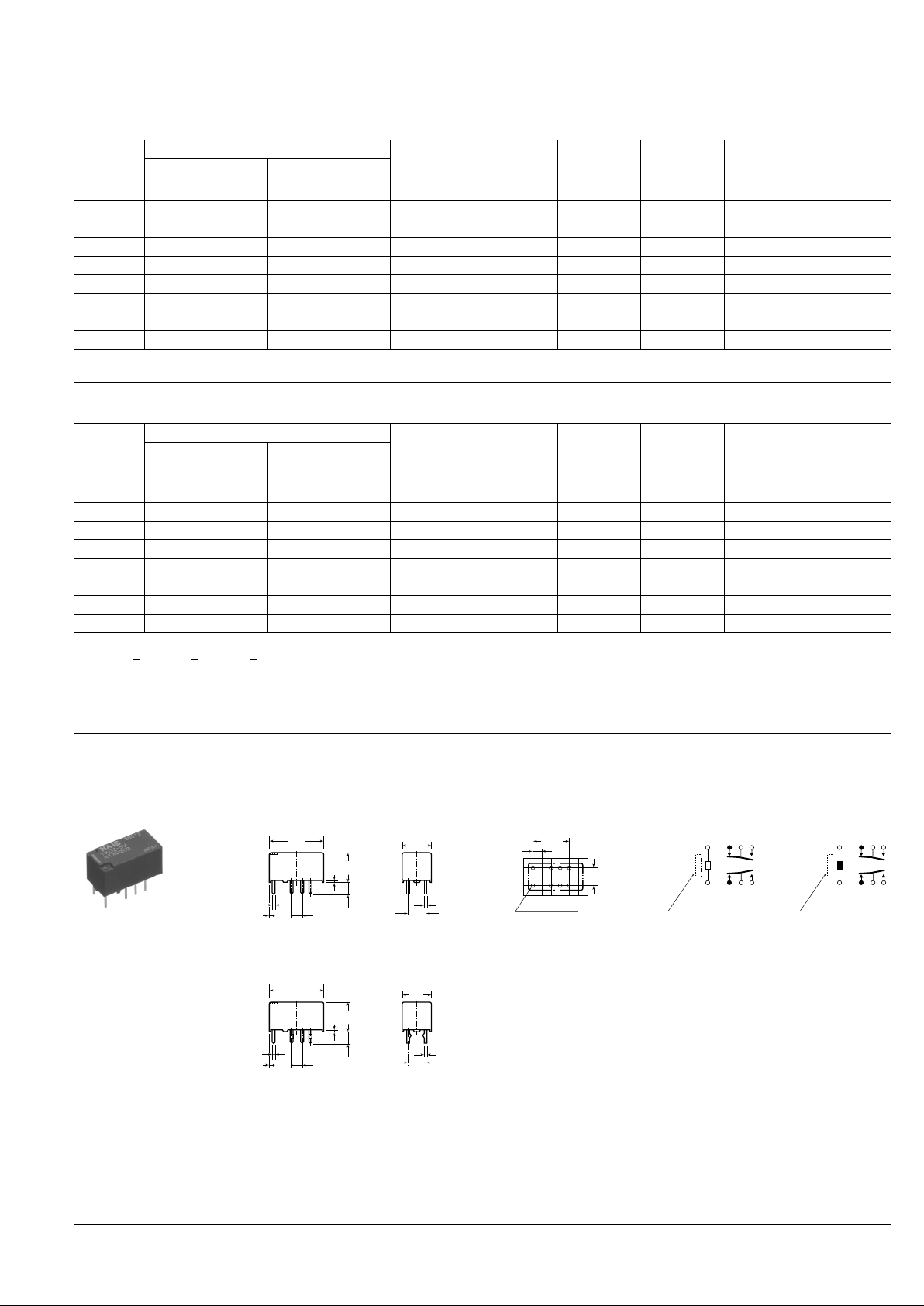
2. M.B.B. Type
(1) Standard PC board terminal and self-clinching terminal
Single side stable
Standard packing: 40 pcs. in an inner package (tube); 1,000 pcs. in an outer package
Coil
Rating,
V DC
Part No.
Pick-up
voltage,
V DC (max.)
Drop-out
voltage,
V DC (min.)
Nominal
operating
current,
mA (±10%)
Coil
resistance,
Ω (±10%)
Nominal
operating
power,
mW
Max.
allowable
voltage,
V DC
Standard PC board
terminal
Self-clinching
terminal
1.5 TXD2-2M-1.5V TXD2-2M-H-1.5V 1.13 0.15 166.7 9 250 1.8
3 TXD2-2M-3V TXD2-2M-H-3V 2.25 0.3 83.3 36 250 3.6
4.5 TXD2-2M-4.5V TXD2-2M-H-4.5V 3.38 0.45 55.6 81 250 5.4
5 TXD2-2M-5V TXD2-2M-H-5V 3.75 0.5 50.0 100 250 6
6 TXD2-2M-6V TXD2-2M-H-6V 4.5 0.6 41.7 144 250 7.2
9 TXD2-2M-9V TXD2-2M-H-9V 6.75 0.9 27.8 324 250 10.8
12 TXD2-2M-12V TXD2-2M-H-12V 9 1.2 20.8 576 250 14.4
24 TXD2-2M-24V TXD2-2M-H-24V 18 2.4 11.3 2,133 270 28.8
(2) Surface-mount terminal
Single side stable
❍: For each surface-mounted terminal variation, input the following letter.
SA type: A
, SL type: L , SS type: S
Standard packing: 40 pcs. (tube), 500 pcs. (tape and reel) in an inner package; 1,000 pcs. in an outer package
Notes:
1. Tape and reel packing symbol "-Z" is not marked on the relay. "X" type tape and reel packing (picked from 1/3/4/5-pin side) is also available.
2. In case of 5 V transistor drive circuit, it is recommended to use 4.5 V type relay.
Coil
Rating,
V DC
Part No.
Set voltage,
V DC (max.)
Reset
voltage,
V DC (min.)
Nominal
operating
current,
mA (±10%)
Coil
resistance,
Ω (±10%)
Nominal
operating
power,
mW
Max.
allowable
voltage,
V DC
Tube packing
Tape and reel
packing
1.5 TXD2S❍-2M-1.5V TXD2S❍-2M-1.5V-Z 1.13 0.15 166.7 9 250 1.8
3 TXD2S❍-2M-3V TXD2S❍-2M-3V-Z 2.25 0.3 83.3 36 250 3.6
4.5 TXD2S❍-2M-4.5V TXD2S❍-2M-4.5V-Z 3.38 0.45 55.6 81 250 5.4
5 TXD2S❍-2M-5V TXD2S❍-2M-5V-Z 3.75 0.5 50.0 100 250 6
6 TXD2S❍-2M-6 TXD2S❍-2M-6V-Z 4.5 0.6 41.7 144 250 7.2
9 TXD2S❍-2M-9 TXD2S❍-2M-9V-Z 6.75 0.9 27.8 324 250 10.8
12 TXD2S❍-2M-12 TXD2S❍-2M-12V-Z 9 1.2 20.8 576 250 14.4
24 TXD2S❍-2M-24 TXD2S❍-2M-24V-Z 18 2.4 11.3 2,133 270 28.8
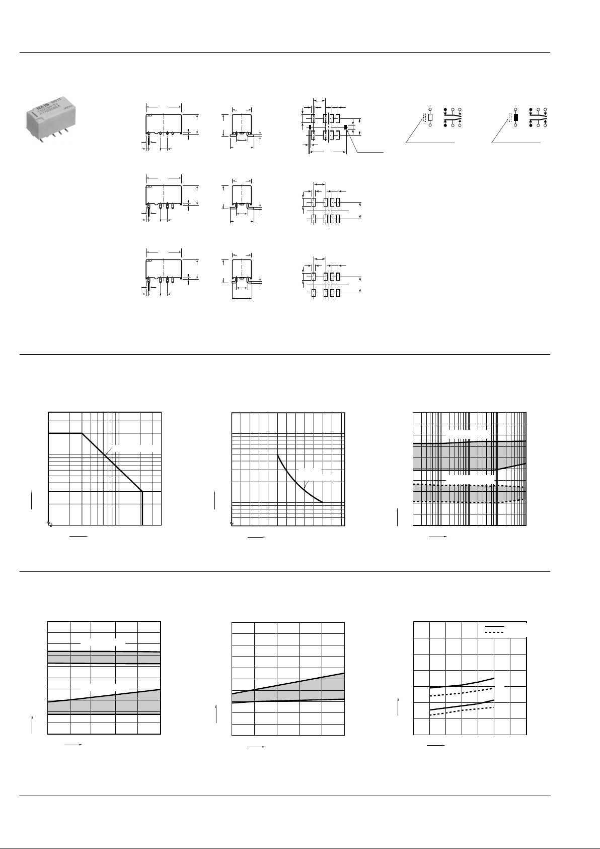
DIMENSIONS
1. Standard PC board terminal and self-clinching terminal
Standard PC board terminal
0.5
.020
1.15
.045
5.08
.200
2.54
.100
8.2
.323
3.5
.138
0.65
.026
7.4
.291
5.08
.200
0.25
.010
15
.591
mm inch
Self clinching terminal
General tolerance: ±0.3 ±.012
0.5
.020
1.15
.045
5.08
.200
2.54
.100
8.2
.323
3.5
.138
0.65
.026
7.4
.291
5.08
.200
0.25
.010
15
.591
PC board pattern
(Copper side view)
Tolerance: ±0.1 ±.004
5.08
.200
2.54
.100
8-1.0 dia
8-.039 dia
10.16
.400
Schematic (Bottom view)
Single side stable
(Deenergized condition)
1 coil latching
(Reset condition)
*Orientation stride located on top of relay.
Direction indication*
12 10 9 8
1 3 4 5
+
–
Direction indication*
12 10 9 8
1 3 4 5
+
–
Page 5
TX-D
164
REFERENCE DATA
1. Maximum switching capacity 2. Life curve 3. Mechanical life
Tested sample: TXD2-5V, 10 pcs.
Operating frequency: 180 cpm
0.2
0.3
0.4
0.5
1.0
2.0
3.0
20 30 50 100 200 3000
Contact voltage, V
DC resistive load
Switching current, A
1.0 2.0
100
50
30
20
10
0
30V DC
resistive load
Switching current, A
No. of operations ×10
4
0 10 100 1000 10000
Max.
Min.
Min.
Max.
0
10
20
30
40
50
60
70
80
90
100
No. of operations, ×10
4
Ratio against the rated voltage, %V
Pick-up voltage
Drop-out voltage
4. Electrical life (2 A 30 V DC resistive load)
Tested sample: TXD2-5V, 6 pcs.
Operating frequency: 20 cpm
Change of pick-up and drop-out voltage Change of contact resistance
5-(1). Coil temperature rise
Tested sample: TXD2-5V, 6 pcs.
Measured portion: Inside the coil
Ambient temperature: 25°C 77°F, 70°C 158°F
0246810
Max.
Min.
Max.
Min.
No. of operations, ×10
4
0
10
20
30
40
50
60
70
80
90
100
Ratio against the rated voltage, %V
Pick-up voltage
Drop-out voltage
0246810
Max.
Min.
No. of operations, ×10
4
0
10
20
30
40
50
60
70
80
90
100
Contact resistance, mΩ
70
60
50
40
30
20
10
0
100 110 120
2A
0A
0A
Coil applied voltage, %V
Temperature rise, °C
2A
+
25°C +77°F
+
70°C +158°F
2. Surface-mount terminal
SA type
0.5
.020
5.08
.200
2.54
.100
8.2
.323
8.4
.331
0.65
.026
7.4
.291
5.08
.200
0.25
.010
15
.591
9.4±0.5
.370±.020
SL type
0.5
.020
5.08
.200
2.54
.100
8.2
.323
0.65
.026
7.4
.291
5.08
.200
0.25
.010
15
.591
9.4±0.5
.370±.020
Max.
10.0
.390
SS type
General tolerance: ±0.3 ±.012
0.5
.020
5.08
.200
2.54
.100
8.2
.323
0.65
.026
7.4
.291
5.08
.200
0.25
.010
15
.591
7.4±0.5
.291±.020
Max.
10.0
.390
mm inch
Suggested mounting pad
(Top view)
0.3
.012
3.16
.124
1
.039
2.54
.100
5.08
.200
1.6
.0.63
7.24
.285
15
.591
For glue-pad
3.16
.124
1
.039
2.54
.100
5.08
.200
7.24
.285
Tolerance: ±0.1 ±.004
2.16
.085
1
.039
2.54
.100
5.08
.200
6.24
.246
Schematic (Top view)
Single side stable
(Deenergized condition)
1 coil latching
(Reset condition)
Direction indication
+
–
12 10 9 8
1 3 4 5
Direction indication
+
–
12 10 9 8
1 3 4 5
Page 6
TX-D
165
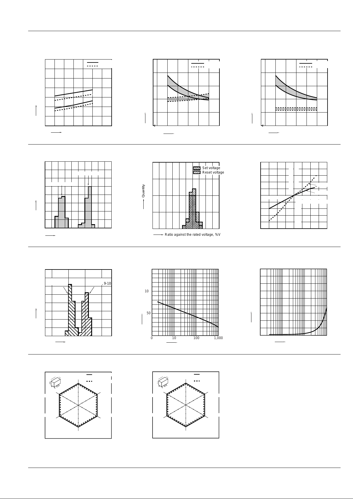
5-(2). Coil temperature rise
Tested sample: TXD2-24V, 6 pcs.
Measured portion: Inside the coil
Ambient temperature: 25°C 77°F, 70°C 158°F
6-(1). Operate/release time characteristics
(with diode)
Tested sample: TXD2-5V, 10 pcs.
6-(2). Operate/release time characteristics
(without diode)
Tested sample: TXD2-5V, 10 pcs.
70
60
50
40
30
20
10
0
2A
0A
0A
100 110 120
Coil applied voltage, %V
Temperature rise, °C
2A
+
25°C +77°F
+
70°C +158°F
1
2
4
5
70 80 100 120
0
3
90 110
Max.
Max.
Min.
Min.
Coil applied voltage, %V
Operate and release time, ms
Release time
Operate time
1
2
4
5
70 80 100 120
0
3
90 110
Max.
Max.
Min.
Min.
Coil applied voltage, %V
Operate and release time, ms
Release time
Operate time
7. Distribution of pick-up and drop-out voltage
Tested sample: TXD2-5V, 50 pcs.
8. Distribution of set and reset voltage
Tested sample: TXD2-L-12V, 30 pcs.
9. Ambient temperature characteristics
Tested sample: TXD2-5V, 5 pcs.
0 102030405060708090100
35
30
25
20
15
10
5
Drop-out voltage
Pick-up voltage
Ratio against the rated voltage, %V
Quantity
0102030405060708090100
15
10
5
,,
,,,,
,,,,,,
,,,,,,
Ratio against the rated voltage, %V
Quantity
Set voltage
Reset voltage
x
x
Variation ratio, %
40
20
–20
–40
–40 200–20 40 60 80
Drop-out voltage
Pick-up voltage
Ambient temperature, °C
10. Distribution of contact resistance
Tested sample: TXD2-5V, 30 pcs. (30 × 4 contacts)
11-(1). High-frequency characteristics
Isolation characteristics
Tested sample: TXD2-12V, 2 pcs.
11-(2). High-frequency characteristics
Insertion loss characteristics
Tested sample: TXD2-12V, 2 pcs.
020304050
35
30
25
20
15
10
5
,
Contact resistance, mΩ
Quantity
Terminal
Nos. 4-5, 8-9
Terminal
Nos. 3-4, 9-10
50
100 100 1,000
100
Frequency, MHz
Isolation, dB
0.6
100 100 1,000
0.2
0.4
1.0
0.8
Frequency, MHz
Insertion loss, dB
12-(1). Malfunctional shock (single side stable)
Tested sample: TXD2-5V, 6 pcs
12-(2). Malfunctional shock (latching)
Tested sample: TXD2-L-12V, 6 pcs.
Y'
Y
XZ
Z' X'
Y
Y'
Z'
Z
X
X'
1000m/s
2
2
2
2
2
1000m/s
2
1000m/s
1000m/s
1000m/s
1000m/s
Deenergized
condition
Energized condition
Y'
Y
XZ
Z' X'
Y
Y'
Z'
Z
X
X'
1000m/s
2
2
2
2
2
1000m/s
2
1000m/s
1000m/s
1000m/s
1000m/s
Reset state
Set state
Page 7
TX-D
166
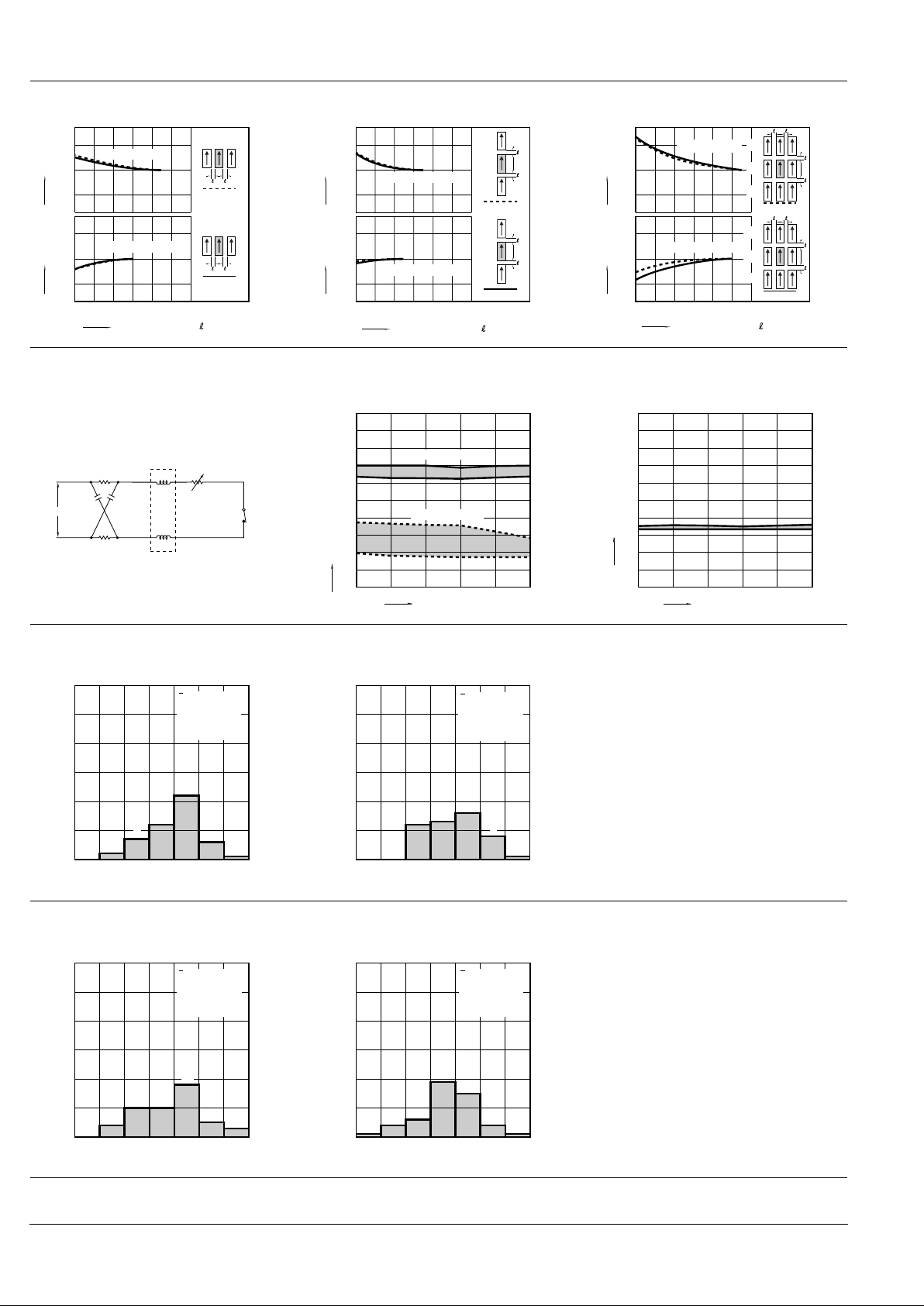
13-(1). Influence of adjacent mounting
Tested sample: TXD2-12V, 6 pcs.
13-(2). Influence of adjacent mounting
Tested sample: TXD2-12V, 6 pcs.
13-(3). Influence of adjacent mounting
Tested sample: TXD2-12V, 6 pcs.
–5
0
5
–5
0
5
ON ON
ON
OFF OFF
OFF
10
.394
6
.236
2
.0794.1578.315
0
Inter-relay distance , mm inch
Rate of change, % Rate of change, %
Pick-up voltage
Drop-out voltage
–5
0
5
–5
0
5
ON
ON
ON
OFF
OFF
OFF
010
.394
6
.236
2
.0794.1578.315
Inter-relay distance , mm inch
Rate of change, % Rate of change, %
Pick-up voltage
Drop-out voltage
–5
0
5
–5
0
5
ON
OFF
0
ON
ON
OFF
OFF
ON
OFF
10
.394
6
.236
2
.0794.1578.315
Inter-relay distance , mm inch
Rate of change, % Rate of change, %
Pick-up voltage
Drop-out voltage
14. Actual load test (35 mA 48 V DC wire spring
relay load)
Tested sample: TXD2-5V, 6 pcs.
Circuit
Change of pick-up and drop-out voltage Change of contact resistance
48 V DC
458 Ω
0.08µF0.08
µF
458 Ω
4
3
TXD
+
–
Wire spring relay
0 1020304050
Max.
Min.
Max.
Min.
0
10
20
30
40
50
60
70
80
90
100
No. of operation, ×10
4
Ratio against the rated voltage, %V
Pick-up voltage
Drop-out voltage
0 1020304050
Max
Min.
0
10
20
30
40
50
60
70
80
90
100
No. of operation, ×10
4
Contact resistance, mΩ
15-(1). Distribution of M.B.B. time
Tested sample: TXD2-2M-5V, 50 pcs.
Terminal No. 3-4-5: ON Terminal No. 3-4-5: OFF
60
50
40
30
20
10
0
2
7
12
22
6
1
100 150 200 250 300 350 400
150 200 250 300 350 400 450
µs min.
µs max.
~
~
~
~
~
~
~
x:
σ
n-1:
Min.:
Max.:
300.5 µs
55.3 µs
165 µs
415 µs
60
50
40
30
20
10
0
12
13
16
8
1
100 150 200 250 300 350 400
150 200 250 300 350 400 450
~
~
~
~
~
~
~
x:
σ
n-1:
Min.:
Max.:
298.8 µs
51.8 µs
205 µs
432 µs
µs min.
µs max.
15-(2). Distribution of M.B.B. time
Tested sample: TXD2-2M-5V, 50 pcs.
Terminal No. 8-9-10: ON Terminal No. 8-9-10: OFF
60
50
40
30
20
10
0
4
10 10
18
5
3
100 150 200 250 300 350 400
150 200 250 300 350 400 450
~
~
~
~
~
~
~
x:
σ
n-1:
Min.:
Max.:
293.4 µs
60.4 µs
155 µs
445 µs
µs min.
µs max.
60
50
40
30
20
10
0
1
4
6
19
15
4
1
100 150 200 250 300 350 400
150 200 250 300 350 400 450
~
~
~
~
~
~
~
x:
σ
n-1:
Min.:
Max.:
281.4 µs
50.8 µs
420 µs
421 µs
µs min.
µs max.
For Cautions for Use, see Page 178 and 179.
9/1/2000 All Rights Reserved, © Copyright Matsushita Electric Works, Ltd.
Go To Online Catalog
 Loading...