

Page 1
®
· Designed for Short-Range Wireless Data Communications
· Supports RF Data Transmission Rates Up to 115.2 kbps
· 3 V, Low Current Operation plus Sleep Mode
· Stable, Easy to Use, Low External Parts Count
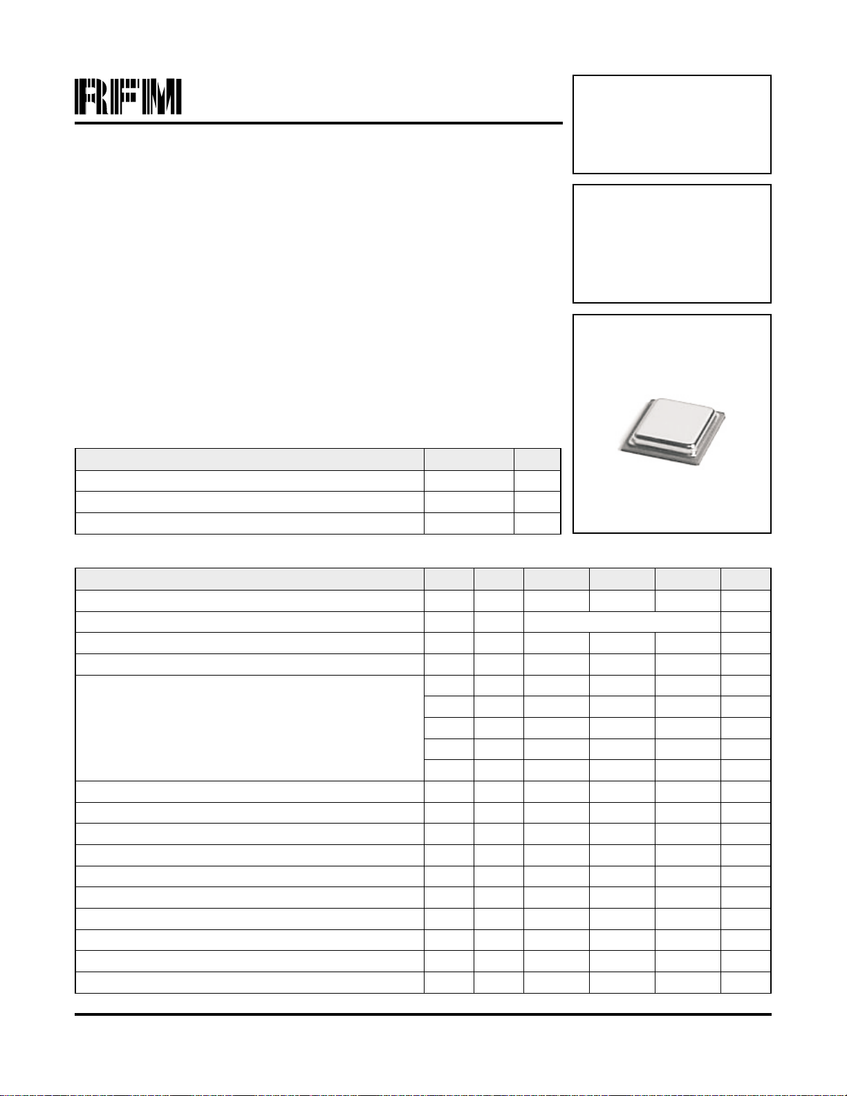
TX5000
433.92 MHz
Hybrid
The TX5000 hybrid transmitter is ideal for short-range wireless data applications
Transmitter
where robust operation, small size, low power consumption and low cost are required.
All critical RF functions are contained in the hybrid, simplifying and speeding designin. The TX5000 includes provisions for both on-off keyed (OOK) and amplitude-shift
keyed (ASK) modulation. The TX5000 employs SAW filtering to suppress output har
-
monics, facilitating compliance with ETSI I-ETS 300 220 and similar regulations.
Absolute Maximum Ratings
Rating Value Units
Power Supply and All Input/Output Pins -0.3 to +4.0 V
o
Non-Operating Case Temperature -50 to +100
Soldering Temperature (10 seconds) 250
Electrical Characteristics
Characteristic Sym Notes Minimum Typical Maximum Units
Operating Frequency f
Modulation Types OOK & ASK
OOK Data Rate 10 kbps
ASK Data Rate 115.2 kbps
Transmitter Performance
Peak RF Output Power, 250 µA TXMOD Current P
Peak Current, 250 µA TXMOD Current I
OOK Turn On/Turn Off Times t
ASK Output Rise/Fall Times t
nd-4th
2
Harmonic Outputs -50 dBm
th
5
-10thHarmonic Outputs -55 dBm
Non-harmonic Spurious Outputs -50 dBm
Sleep Mode Current I
Sleep to Transmit Switch Time t
Transmit to Sleep Switch Time t
Control Input Logic Low Level 200 mV
Control Input Logic High Level 1 Vcc - 300 mV
Power Supply Voltage Range V
Operating Ambient Temperature T
O
O
TP
ON/tOFF
TR/tTF
S
TOR
RTO
CC
A
C
o
C
433.72 434.12 MHz
0 dBm
7.5 mA
20/15 µs
1.1/1.1 µs
0.7 µA
21 µs
15 µs
2.2 3.7 Vdc
-40 +85
o
C
1
Page 2
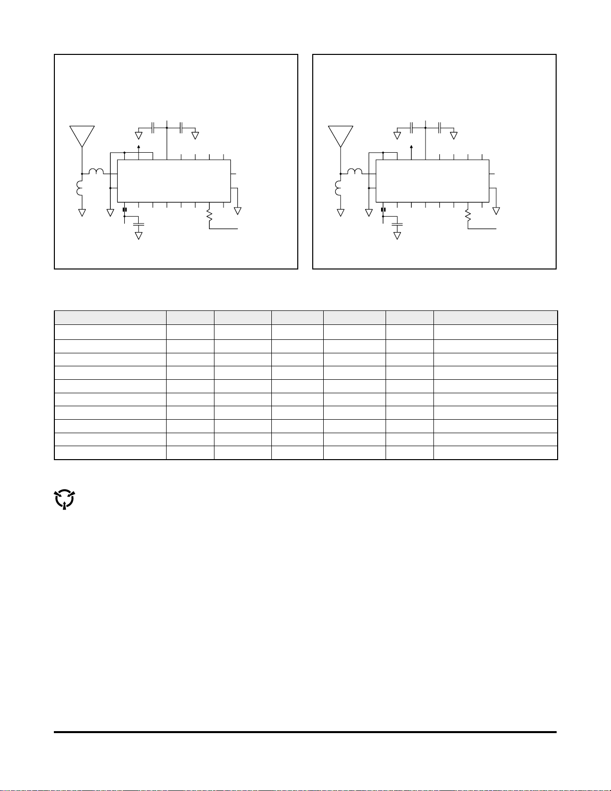
Transm itter O O K Configuration
Transm itter ASK Configuration
+ 3
VDC
C
C
T/S
GND3CNT
L
AT
20
L
ESD
1
CNT
RL0
RL1PWIDTHPRATE
RFIO
GND1
AGC
VCC
DET
CAP
1
23456789
L
RFB
C
RFB1
+ 3
VDC
RFB2
TOP VIEW
PK
VCC
DCB
+
2
RX
CMP
DATA
INBBOUT
R
TXM
Transmitter Set-Up, 3.0 Vdc, -40 to +850C
Item Symbol OOK ASK ASK Units Notes
DR
Nominal NRZ Data Rate
Minimum Signal Pulse SP
Maximum Signal Pulse SP
TXMOD Resistor R
DC Bypass Capacitor C
RF Bypass Capacitor 1 C
RF Bypass Capacitor 2 C
RF Bypass Bead L
Series Tuning Inductor L
Shunt Tuning/ESD Inductor L
NOM
MIN
MAX
TXM
DCB
RFB1
RFB2
RFB
AT
ESD
+ 3
VDC
C
THLD1THLD
RREF
GND2
TX
LPF
MOD
ADJ
1213141516171819
2
11
10
M odulation Input
C
GND3CNT
L
AT
20
L
ESD
1
CNT
RL0
RL1PWIDTHPRATE
RFIO
GND1
AGC
VCC
DET
CAP
1
23456789
L
RFB
C
RFB1
+ 3
VDC
RFB2
T/S
TOP VIEW
PK
VCC
DCB
+
1213141516171819
THLD1THLD
2
CMP
DATA
INBBOUT
2
RREF
11
GND2
10
TX
RX
LPF
MOD
ADJ
R
TXM
2.4 19.2 115.2 kbps see page 1
416.67 52.08 8.68 µs single bit
1666.68 208.32 34.72 µs 4 bits of same value
8.2 8.2 8.2 K ±5%, for 0 dBm output
4.7 4.7 4.7 µF tantalum
27 27 27 pF ±5% NPO
100 100 100 pF ±5% NPO
Fair-Rite Fair-Rite Fair-Rite vendor 2506033017YO or equivalent
56 56 56 nH 50 ohm antenna
220 220 220 nH 50 ohm antenna
M odulation Input
CAUTION: Electrostatic Sensitive Device. Observe precautions when handling.
Notes:
1. Do not allow the voltage applied to a control input pin to exceed Vcc + 200 mV.
2. The companion receiver to the TX6000 is the RX6000. Please see RFM’s web site at www.rfm.com for details.
2
Page 3
Transmitter Theory of Operation
Introduction
RFM’s TX-series hybrid transmitters are specifically designed for
short-range wireless data communication applications. These trans
mitters provide robust operation, very small size, low power con
sumption and low implementation cost. All critical RF functions are
contained in the hybrid, simplifying and speeding design-in. The
transmitters can be readily configured to support a wide range of
data rates and protocol requirements. TX-series transmitters feature
excellent suppression of output harmonics and virtually no other RF
emissions, making them easy to certify to short- range (unlicensed)
radio regulations.
Transmitter Block Diagram
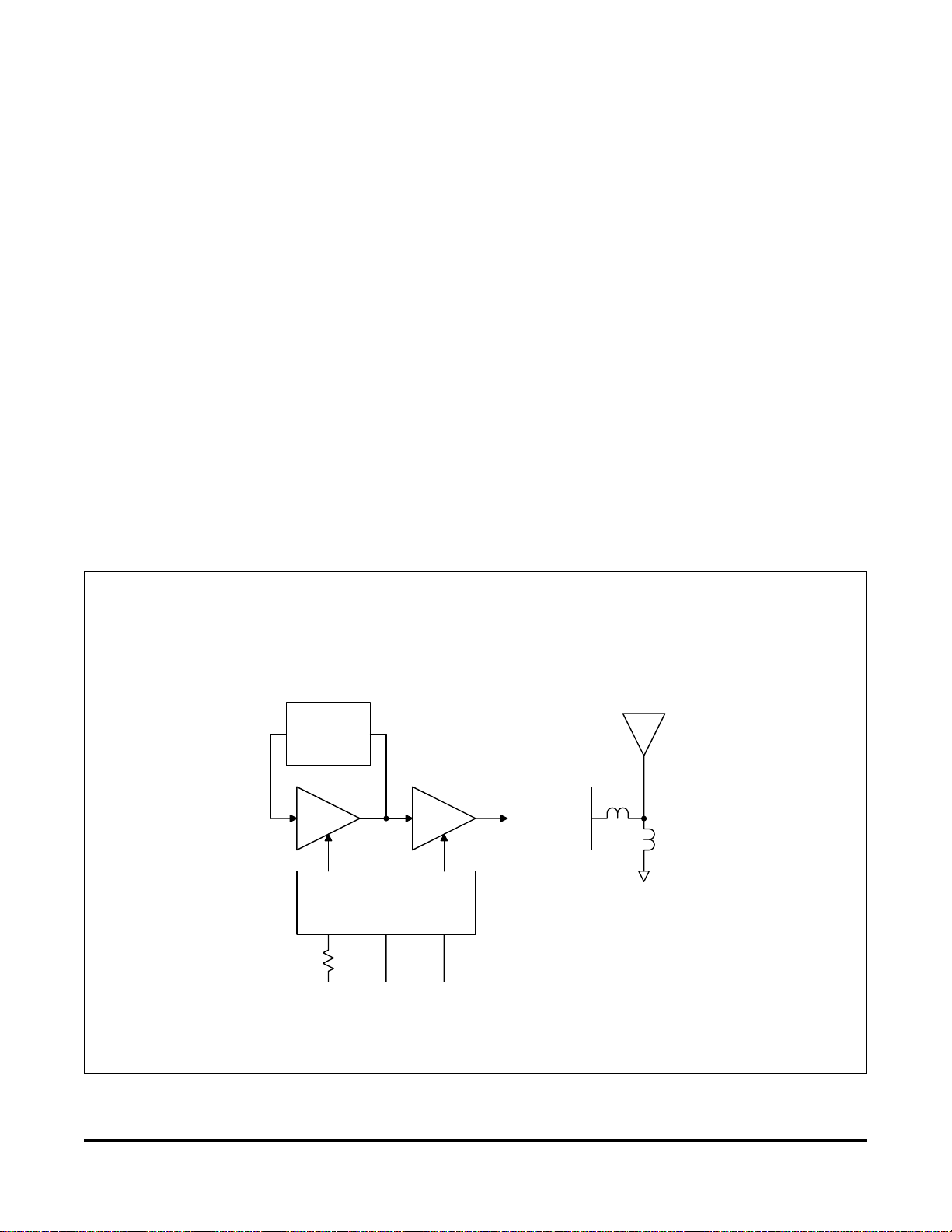
Figure 1 is the general block diagram of the transmitter. Please refer
to Figure 1 for the following discussions.
Antenna Port
The only external RF components needed for the transmitter are the
antenna and its matching components. Antennas presenting an im
pedance in the range of 35 to 72 ohms resistive can be satisfactorily
matched to the RFIO pin with a series matching coil and a shunt
matching/ESD protection coil. Other antenna impedances can be
matched using two or three components. For some impedances,
two inductors and a capacitor will be required. A DC path from RFIO
to ground is required for ESD protection.
-
Transmitter Chain
The transmitter chain consists of a SAW coupled-resonator oscilla
tor followed by a modulated buffer amplifier. The SAW coupled res
onator output filter suppresses transmitter harmonics to the
antenna.
Transmitter operation supports two modulation formats, on-off
keyed (OOK) modulation, and amplitude-shift keyed (ASK) modula
tion. When OOK modulation is chosen, the transmitter output turns
completely off between “1” data pulses. When ASK modulation is
chosen, a “1” pulse is represented by a higher transmitted power
level, and a “0” is represented by a lower transmitted power level.
OOK modulation provides compatibility with first-generation ASH
technology, and provides for power conservation. ASK modulation
must be used for high data rates (data pulses less than 200 µs).
ASK modulation also reduces the effects of some types of interfer
ence and allows the transmitted pulses to be shaped to control mod
ulation bandwidth.
The modulation format is chosen by the state of the CNTRL0 and
the CNTRL1 mode control pins, as discussed below. In the OOK
mode, the oscillator amplifier TXA1 and buffer amplifier TXA2 are
-
turned off when the voltage to the TXMOD input falls below 220 mV.
In the OOK mode, the data rate is limited by the 20/15 µs turn-on
and turn-off time of the oscillator. In the ASK mode TXA1 is biased
ON continuously, and the output of TXA2 is modulated by the
TXMOD input current. Minimum output power occurs in the ASK
mode when the modulation driver sinks about 10 µA of current from
the TXMOD pin.
-
-
-
-
-
Transm itter B lock D iagram
SAW
Coupled
R esonator
TXA1 TXA2
M odulation
& Bias Control
R
TXM
TX
IN
CN
TRL1CNTRL0
Figure 1
SAW
CR
F ilte r
Antenna
Ant
Tune
Tune/E S D
3
Page 4
The transmitter RF output power is proportional to the input current
to the TXMOD pin. A series resistor is used to adjust the peak trans
mitter output power. 0 dBm of output power requires about 250 µA
of input current.
Transmitter Mode Control
The three transmitter operating modes – transmit ASK, transmit
OOK, and power-down (sleep), are controlled by the Modulation &
Bias Control function, and are selected with the CNTRL1 and
CNTRL0 control pins. Setting CNTRL1 high and CNTRL0 low place
the unit in the ASK transmit mode. Setting CNTRL1 low and
CNTRL0 high place the unit in the OOK transmit mode. Setting
CNTRL1 and CNTRL0 both low place the unit in the power-down
mode. (Note that the resistor driving TXMOD must also be low in the
power-down mode to minimize power-down current.) CNTRL1 and
CNTRL0 are CMOS compatible inputs. These inputs must be held
at a logic level; they cannot be left unconnected.
Turn-On Timing
The maximum time required for either the OOK or ASK transmitter
mode to become operational is 5 ms after the supply voltage
reaches 2.2 Vdc. The total turn-on time to stable transmitter opera
tion for a 10 ms power supply rise time is 15 ms.
Sleep and Wake-Up Timing
The maximum transition time from either transmit mode to the sleep
and t
mode (t
TOS
) is 15 µs after CNTRL1 and CNTRL0 are both
TAS
low (1 µs fall time).
The maximum time required to switch from the sleep mode to either
and t
transmit mode (t
STO
) is 21 µs. Most of this time is due to the
STA
start-up of the transmitter oscillator.
-
0.43"
(10.9)
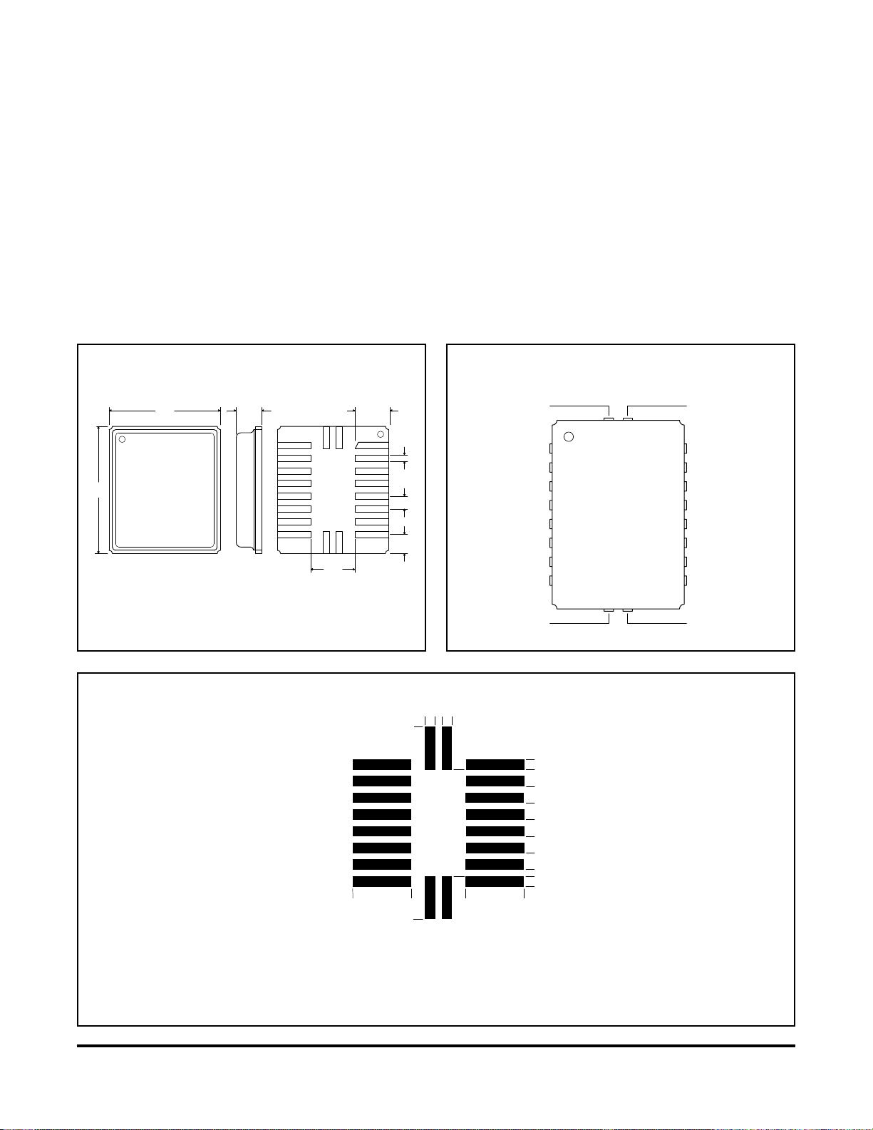
SM -20L P ackage D raw in g
0.38"
(9.65)
0.08"
(2.03)
0.13"
(3.30)
0.125"
(3 .20 )
0.02"
(0 .51 )
0.04"
(1 .02 )
0.075"
(1 .90 )
.4 6 0 0
Transm itter P in O ut
19
18
17
16
15
14
13
12
RFIO
GND3
CNTRL0
CNTRL1
VCC2
NC
NC
NC
NC
GND1
201
2
VCC1
3
NC
4
NC
5
NC
6
NC
7
NC
8
TXM O D NC
NC
9
10
11
GND2
.1 9 7 5
.2 1 2 5
.2 3 7 5
.1 7 2 5
.3 8 2 5
.3 5 7 5
.3 1 7 5
.2 7 7 5
.2 3 7 5
.1 9 7 5
.1 5 7 5
.1 1 7 5
.1 0 2 5
.0 7 7 5
0.000
.1 4 0
0.000
D im ensions in inches
S M -2 0 L P C B P a d L a y o u t
4
.2 7 0
.4 1 0
Page 5
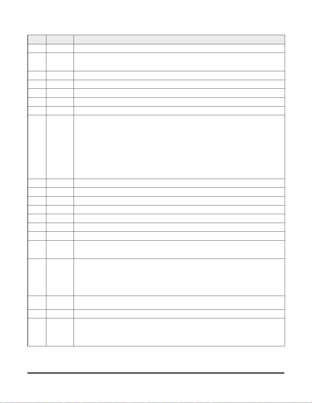
Pin Descriptions
Pin Name Description
1 GND1 GND1 is the RF ground pin. GND2 and GND3 should be connected to GND1 by short, low-inductance traces.
2 VCC1
VCC1 is usually connected to the positive supply through a ferrite RF decoupling bead which is bypassed by an
RF capacitor on the supply side. See the description of VCC2 (Pin 16) for additional information.
3 NC No connection. Printed circuit board pad may be grounded or floating.
4 NC No connection. Printed circuit board pad may be grounded or floating.
5 NC No connection. Printed circuit board pad may be grounded or floating.
6 NC No connection. Printed circuit board pad may be grounded or floating.
7 NC No connection. Printed circuit board pad may be grounded or floating.
The transmitter RF output voltage is proportional to the input current to this pin. A series resistor is used to adjust
the peak transmitter output voltage. 0 dBm of output power requires 250 µA of input current. In the ASK mode,
minimum output power occurs when the modulation driver sinks about 10 µA of current from this pin. In the OOK
mode, input signals less than 220 mV completely turn the transmitter oscillator off. Internally, this pin appears to
VCC1 is the positive supply voltage pin for the transmitter output amplifier and the transmitter base-band circuitry.
for a 3 Vdc supply voltage is approxi
O
is in mA
TXM
8 TXMOD
be a diode in series with a small resistor. Peak transmitter output power P
mately:
P
= 16*(I
O
)2, where POis in mW, and the peak modulation current I
TXM
A ±5% resistor value is recommended. In the OOK mode, this pin is usually driven with a logic-level data input
(unshaped data pulses). OOK modulation is practical for data pulses of 200 µs or longer. In the ASK mode, this
pin accepts analog modulation (shaped or unshaped data pulses). ASK modulation is practical for data pulses
8.7 µs or longer. This pin must be low in the power-down (sleep) mode. Please refer to the ASH Transceiver De
signer’s Guide for additional information on modulation techniques.
9 NC No connection. Printed circuit board pad may be grounded or floating.
10 GND2 GND2 is an IC ground pin. It should be connected to GND1 by a short, low inductance trace.
11 NC No connection. Printed circuit board pad may be grounded or floating.
-
-
12 NC No connection. Printed circuit board pad may be grounded or floating.
13 NC No connection. Printed circuit board pad may be grounded or floating.
14 NC No connection. Printed circuit board pad may be grounded or floating.
15 NC No connection. Printed circuit board pad may be grounded or floating.
VCC2 is the positive supply voltage pin for the transmitter oscillator. Pin 16 must be bypassed with an RF capaci
16 VCC2
tor, and must also be bypassed witha1to10µFtantalum or electrolytic capacitor. Power supply voltage ripple
should be limited to 10 mV peak-to-peak. See the ASH Transceiver Designer’s Guide for additional information.
CNTRL1 and CNTRL0 select the transmit modes. CNTRL1 high and CNTRL0 low place the unit in the ASK trans
mit mode. CNTRL1 low and CNTRL0 high place the unit in the OOK transmit mode. CNTRL1 and CNTRL0 both
low place the unit in the power-down (sleep) mode. CNTRL1 is a high-impedance input (CMOS compatible). An
17 CNTRL1
input voltage of 0 to 300 mV is interpreted as a logic low. An input voltage of Vcc - 300 mV or greater is inter
preted as a logic high. An input voltage greater than Vcc + 200 mV should not be applied to this pin. A logic high
requires a maximum source current of 40 µA. A logic low requires a maximum sink current of 25 µA (1 µA in sleep
mode). This pin must be held at a logic level; it cannot be left unconnected.
18 CNTRL0
CNTRL0 is used with CNTRL1 to control the operating modes of the transmitter. See the description of CNTRL1
for more information.
19 GND3 GND3 is an IC ground pin. It should be connected to GND1 by a short, low inductance trace.
RFIO is the transmitter RF output pin. This pin is connected directly to the SAW filter transducer. Antennas pre
senting an impedance in the range of 35 to 72 ohms resistive can be satisfactorily matched to this pin with a se
20 RFIO
ries matching coil and a shunt matching/ESD protection coil. Other antenna impedances can be matched using
two or three components. For some impedances, two inductors and a capacitor will be required. A DC path from
RFIO to ground is required for ESD protection.
-
-
-
-
-
5
Page 6
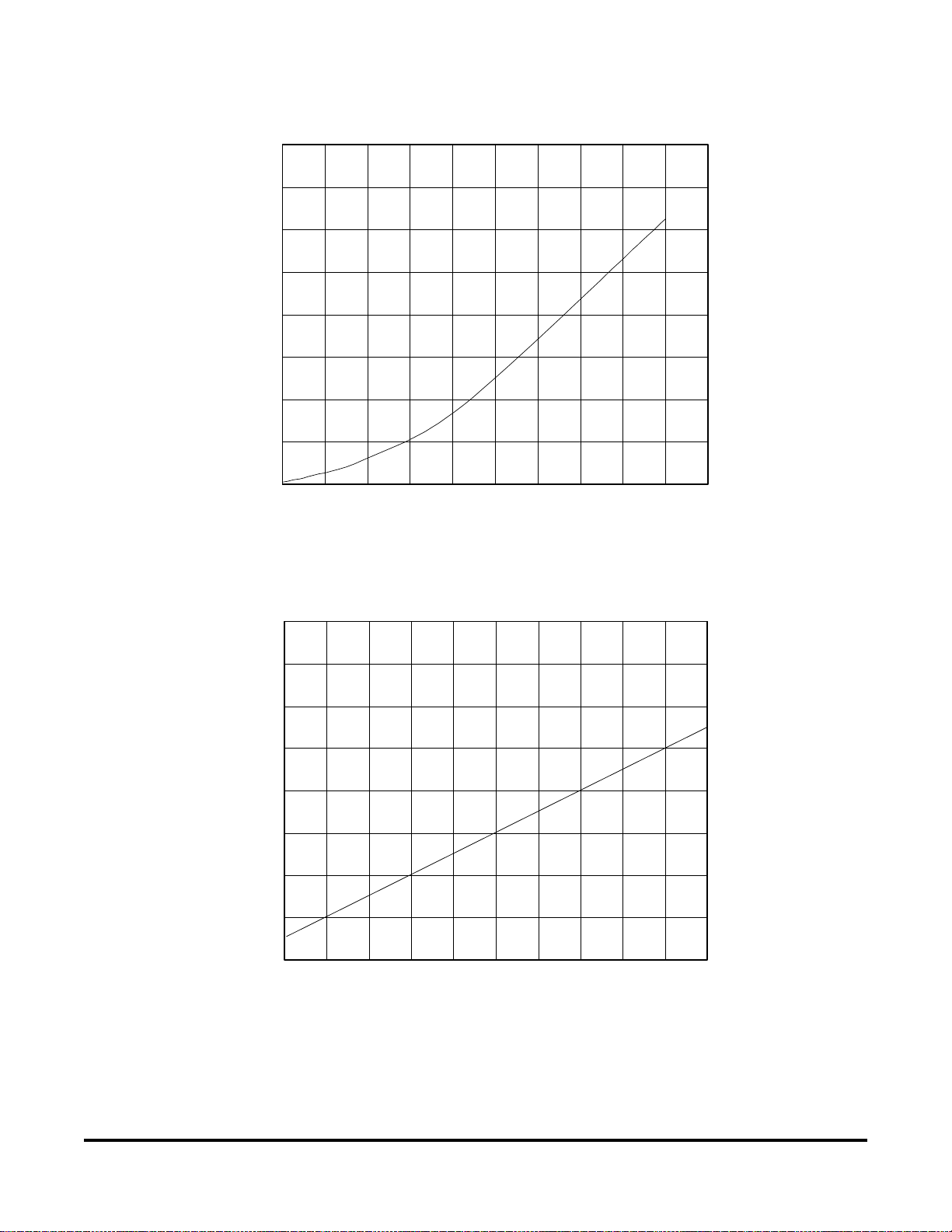
RF O utput Pow er vs I
1.60
1.40
1.20
1.00
0.80
0.60
O u t p u t P o w e r in m W
0.40
0.20
25 50 75 100 125 150 175 200 275250225
I
in µ A
TXM
TXM
3 V
V
v s I
TXM
1.20
1.15
1.10
1.05
in V
1.00
TXM
V
0.95
0.90
0.85
25 50 75 100 125 150 175 200 275250225
I
TXM
TXM
in µ A
Note: Specifications subject to change without notice.
File: tx5000k.vp, 2003.07.20 rev
6
 Loading...