

Page 1
TWL2203
POWER SUPPLY MANAGEMENT IC
SLVS185 – FEBRUAR Y 2000
1
POST OFFICE BOX 655303 • DALLAS, TEXAS 75265
D
Li-Ion Battery Charging Control
D
Over-Voltage Shutdown
D
Seven Low-Dropout Low-Noise Linear
Voltage Regulators (LDO)
D
Voltage Detectors (With Power-Off Delay)
D
Four-Channel Analog Multiplexer
D
Three General-Purpose Operational
Amplifiers
D
Ringer Driver
D
Power Supply Switch for Accessories
D
Low Quiescent Current
D
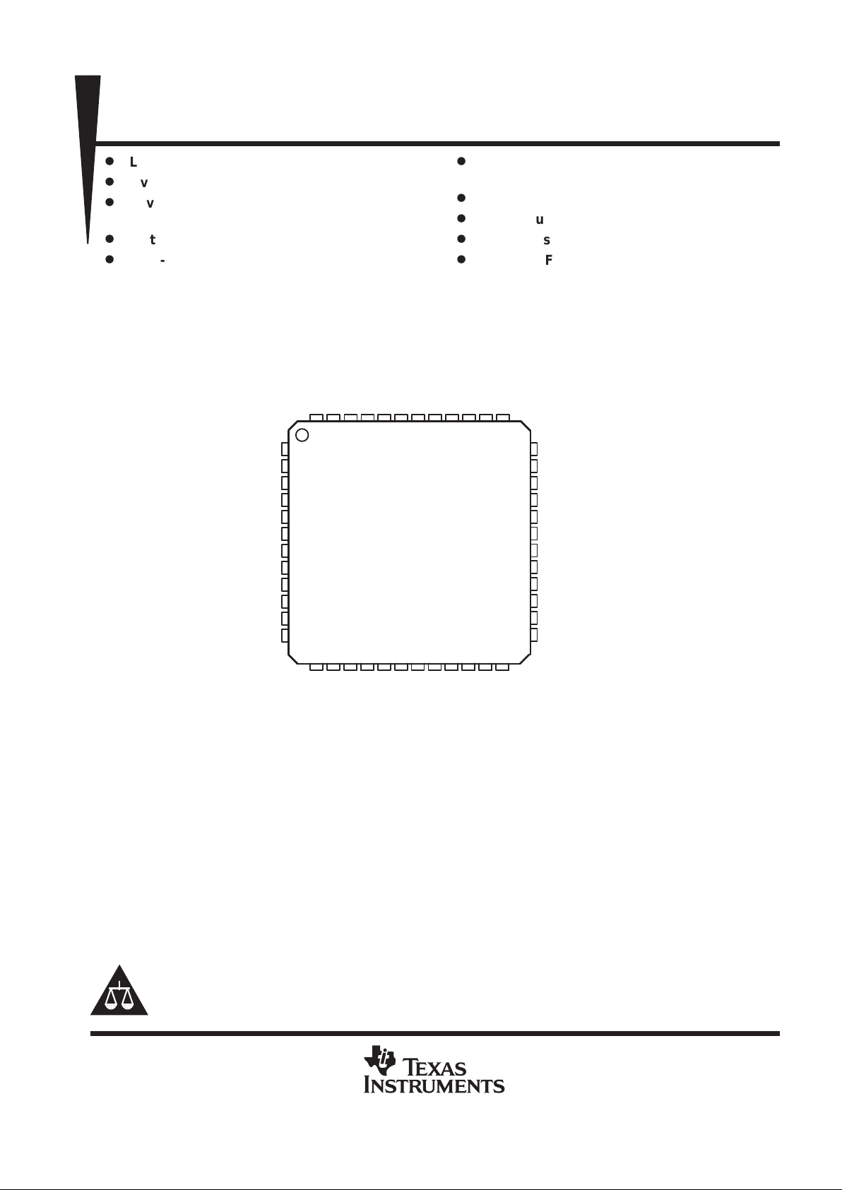
48-pin TQFP
14 15
RINGON
RING
VOUT6
DET_DELAY
VOUT2
V
CC
VSUP
VOUT4
VOUT5
VOUT3
VOUT1
EN3
36
35
34
33
32
31
30
29
28
27
26
25
16
1
2
3
4
5
6
7
8
9
10
11
12
VREF
MUXOUT
MUXIN0
MUX0
MUX1
MUXIN1
MUXIN2
MUXIN3
OP1I–
OP1I+
OP2I–
OP2I+
17 18 19 20
TCOUTVBCH
VG2
47 46 45 44 4348 42
VEXT
IADJ
VG1
ICH+
VOUT7
EN4
EN1
EN2
OP1O
OP3O
GND
DET2
VCH
DET1
40 39 3841
21
22 23 24
37
13
GNDRING
ICH-
ENOP_MUX
OP3I–
OP3I+
OP2O
PFB PACKAGE
(TOP VIEW)
description
The TWL2203 incorporates a complete power-management system for a cellular telephone that uses
lithium-ion cells. The device includes circuitry to control the gate voltage of two P-channel MOSFETs. The
MOSFETs perform constant-voltage/constant-current charging (CVCC). The TWL2203 has seven low-drop
linear voltage regulators (LDO) to regulate the battery power supply to the different sections of the phone, a
battery voltage monitor, a ringer driver , an analog multiplexer , and three general-purpose operational amplifiers
for signal conditioning.
The TWL2203 is packaged in TI’s 48-pin thin-quad flat package (PFB).
Copyright 2000, Texas Instruments Incorporated
PRODUCTION DATA information is current as of publication date.
Products conform to specifications per the terms of Texas Instruments
standard warranty. Production processing does not necessarily include
testing of all parameters.
MicroStar is a trademark of Texas Instruments Incorporated.
Please be aware that an important notice concerning availability, standard warranty, and use in critical applications of
Texas Instruments semiconductor products and disclaimers thereto appears at the end of this data sheet.
Page 2
TWL2203
POWER SUPPLY MANAGEMENT IC
SLVS185 – FEBRUAR Y 2000
2
POST OFFICE BOX 655303 • DALLAS, TEXAS 75265
AVAILABLE OPTIONS
PACKAGE
T
A
PLASTIC THIN-QUAD FLAT PACKAGE
(PFB)
–30°C to 85°C TWL2203PFB
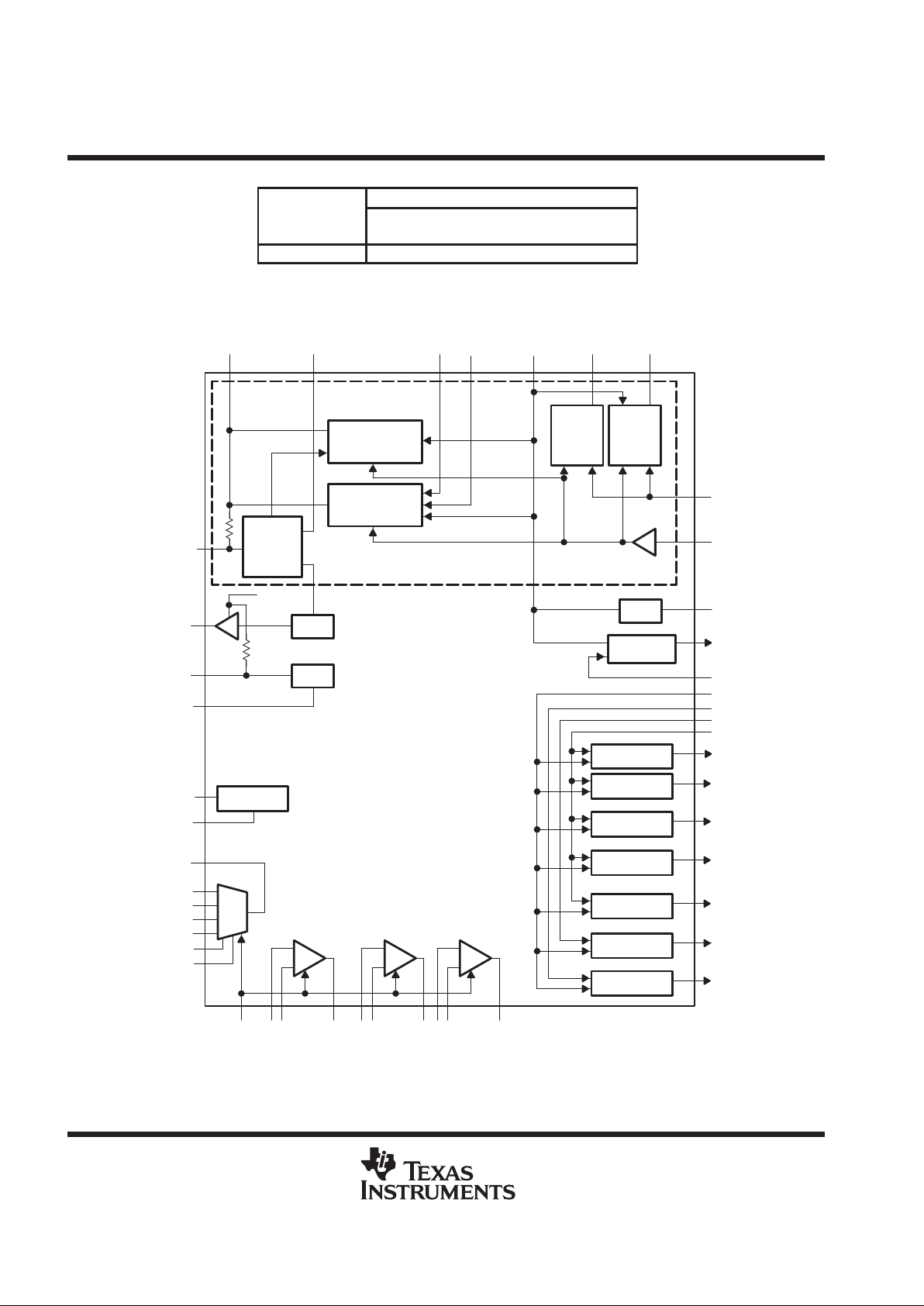
functional block diagram
M
U
X
4.2 V
Regulation
CVCC
Charge
Switch
Control
Trickle
Charge
Current
Control
Current Limit
Control
Over-
Voltage
Shutdown
VDET1
VREF
LDO REG 7
EN4
VDET2
VEXT
DET1
VREF
DET2
DET_DELAY
Power Switch
EN3
EN2
EN1
LDO REG 1
VOUT1
LDO REG 2
VOUT2
LDO REG 3
VOUT3
LDO REG 4
VOUT4
LDO REG 5
VOUT5
LDO REG 6
VOUT6
Ringer DriveRING
RINGON
MUXOUT
MUXIN0
MUXIN1
MUXIN2
MUXIN3
MUX0
MUX1
_
+
_
+
_
+
ENOP_MUX
OP1I+
OP1I–
OP1O
OP12+
OP12–
OP2O
OP12+
OP13–
OP3O
VG1 VCH IADJ ICH+
ICH-
VG2 TCOUT
CH
VB
VSUP
VCC
VOUT7
VOUT2
Page 3
TWL2203
POWER SUPPLY MANAGEMENT IC
SLVS185 – FEBRUAR Y 2000
3
POST OFFICE BOX 655303 • DALLAS, TEXAS 75265
Terminal Functions
TERMINAL
NO.
I/O DESCRIPTION
NAME
QFB
CH 39 I CMOS signal input set to logic high to enable battery-charging function
DET_DELAY 33 I/O Delay programming pin for VDET2
DET1 21 O Voltage detector CMOS output
DET2 19 O Voltage detector output with 40-kΩ pull–up resistor
EN1 23 I Set to logic high to enable LDO regulators 1–4 and power supply switch
EN2 24 I Set to logic high to enable LDO regulator 5
EN3 25 I Set to logic high to enable LDO regulator 6
EN4 22 I Set to logic high to enable LDO regulator 7
ENOP_MUX 42 I Set to logic high to enable the op amps and the analog multiplexer
GND 18 Ground for most sections of the device
GNDRING 37 Ringer ground
IADJ 47 I/O Terminal for gain control of battery-charging current monitor
ICH– 43 I Current-sense input/trickle charge, input/power supply to LDO regulator 7, and reference.
ICH+ 45 I Current-sense input
MUX0 4 I Analog multiplexer channel selector bit-input (logic high is true)
MUX1 5 I Analog multiplexer channel selector bit-input (logic high is true)
MUXIN0 3 I Analog multiplexer input 0
MUXIN1 6 I Analog multiplexer input 1
MUXIN2 7 I Analog multiplexer input 2
MUXIN3 8 I Analog multiplexer input 3
MUXOUT 2 O Analog multiplexer output
OP1I– 9 I Op amp 1 negative input
OP1I+ 10 I Op amp 1 positive input
OP1O 15 O Op amp 1 output
OP2I– 11 I Op amp 2 negative input
OP2I+ 12 I Op amp 2 positive input
OP2O 16 O Op amp 2 output
OP3I– 14 I Op amp 3 negative input
OP3I+ 13 I Op amp 3 positive input
OP3O 17 O Op amp 3 output
RING 35 I Ringer drive input
RINGON 36 I Ringer enable (logic high to enable)
TCOUT 41 O Trickle-charge output
V
B
40 I Battery voltage input for charging control
V
CC
31 Power supply to most of the device
VCH 20 I External power supply input for voltage detection
VEXT 48 I External voltage input
VG1 46 O MOSFET M1 gate drive
VG2 38 O MOSFET M2 gate drive
VOUT1 26 O LDO REG 1 output 1
VOUT2 32 O LDO REG 2 output 2
Page 4
TWL2203
POWER SUPPLY MANAGEMENT IC
SLVS185 – FEBRUAR Y 2000
4
POST OFFICE BOX 655303 • DALLAS, TEXAS 75265
Terminal Functions (Continued)
TERMINAL
NO.
I/O DESCRIPTION
NAME
QFB
VOUT3 27 O LDO REG 3 output 3
VOUT4 29 O LDO REG 4 output 4
VOUT5 28 O LDO REG 5 output 5
VOUT6 34 O LDO REG 6 output 6
VOUT7 44 O LDO REG 7 output 7
VREF 1 O Voltage-reference bypass output
VSUP 30 O Power-supply switch output
detailed description
battery-charging control
The battery charging control block in the device is a part of the lithium-ion battery (Li-Ion) charging system of
the phone. It is capable of regulating the external power source to charge the lithium-ion battery according to
the battery-charging requirements. More information on battery-charging control is presented in the
application
information
section.
The MOSFET driver and its feedback-control circuit are enabled/disabled by a CMOS control signal provided
by the phone’s microprocessor . The maximum-charging current is set by external resistors for design flexibility .
overvoltage shutdown
The device shuts down the charging circuit in the presence of an overvoltage condition.
low-dropout linear voltage regulators
The device has seven separate low-dropout linear-voltage regulators. A single enable signal controls four of
the regulators. The last three regulators are controlled by their own enable signals.
voltage detectors (with power-off delay)
The device has two voltage detectors. The voltage detectors monitor the voltage level of the external power and
V
CC
. The external power detector (VDET1) has a CMOS output. The VCC detector (VDET2) activates on the
falling edge and has user-adjustable power-off delay. There is an internal pullup resistor on the output.
analog multiplexer
The device has a four-channel analog multiplexer with two-bit channel-selector signal input and a shutdown
function. In the shutdown mode, all the input and output terminals are in the high-impedance state.
operational amplifiers
The device has three rail-to-rail operational amplifiers with common shutdown control.
power supply switch for external phone accessories
The device provides current-limited voltage supply to the external phone accessories via the external-interface
connector. The power supply switch is controlled by the same enable signal (EN1) that controls the four
regulators—LDO1-LDO4. The external phone accessories are resistive in nature.
ringer driver
The device is capable of driving a ringer. It is controlled by a CMOS signal, and uses an N-channel low-side
driver.
Page 5
TWL2203
POWER SUPPLY MANAGEMENT IC
SLVS185 – FEBRUAR Y 2000
5
POST OFFICE BOX 655303 • DALLAS, TEXAS 75265
DISSIPATION-RATING TABLE – FREE-AIR TEMPERA TURE
PACKAGE
TA <25°C
POWER RATING
OPERATING FACTOR
ABOVE TA = 25°C
TA = 70°C
POWER RATING
TA = 85°C
POWER RATING
PFB 1962 mW 15.7 mW/°C 1256 mW 1020 mW
absolute maximum ratings over operating free-air temperature (unless otherwise noted)
†
Supply-voltage range, V
CC
–0.3 V to 6.5 V. . . . . . . . . . . . . . . . . . . . . . . . . . . . . . . . . . . . . . . . . . . . . . . . . . . . . . . . .
External-voltage range –0.3 V to 15 V. . . . . . . . . . . . . . . . . . . . . . . . . . . . . . . . . . . . . . . . . . . . . . . . . . . . . . . . . . . . .
Output-voltage range –0.3 V to 6.5 V. . . . . . . . . . . . . . . . . . . . . . . . . . . . . . . . . . . . . . . . . . . . . . . . . . . . . . . . . . . . . .
Input-voltage range, all other pins –0.3 V to 6.5 V. . . . . . . . . . . . . . . . . . . . . . . . . . . . . . . . . . . . . . . . . . . . . . . . . . .
Continuous total-power dissipation See Dissipation-Rating Table. . . . . . . . . . . . . . . . . . . . . . . . . . . . . . . . . . . . . .
Free-air temperature range –30°C to 85°C. . . . . . . . . . . . . . . . . . . . . . . . . . . . . . . . . . . . . . . . . . . . . . . . . . . . . . . . .
Storage-temperature range –65°C to 150°C. . . . . . . . . . . . . . . . . . . . . . . . . . . . . . . . . . . . . . . . . . . . . . . . . . . . . . . .
†
Stresses beyond those listed under “absolute maximum ratings” may cause permanent damage to the device. These are stress ratings only, and
functional operation of the device at these or any other conditions beyond those indicated under “recommended operating conditions” is not
implied. Exposure to absolute-maximum-rated conditions for extended periods may affect device reliability.
recommended operating conditions
PARAMETER TEST CONDITIONS MIN TYP MAX UNIT
pp
In regulation 2.85 3.75 4.25
Suppl
y v
oltage, V
CC
In transient condition 2.85 6
V
Allowable range 0 5.5 12
VEXT
Normal charging operation 4.6 5.5 6
V
VCH 2.1 6 V
High-level logic input, V
IH
2.1 V
Low-level logic input, V
IL
0.9 V
electrical characteristics over recommended operating junction temperature range, VCC = 3.75 V
and VEXT = 5.5 V (unless otherwise specified)
current table, TA = –40°C to 85°C
PARAMETER TEST CONDITIONS MIN TYP MAX UNIT
Shutdown current
EN1 = EN2 = EN3 = EN4 = ENOP_MUX = VCH =
CH = RINGON = VEXT = GND
50 90
Quiescent current
LDOreg. 1–4, power-switch quiescent current
EN1 = VOUT2, EN2 = EN3 = EN4 = ENOP_MUX
= VCH = CH = RINGON = VEXT = GND
210 350
Quiescent current
LDOreg. 1–5, power-switch quiescent current
EN1 = EN2 = VOUT2, EN3 = EN4 = ENOP_MUX
= VCH = CH = RINGON = VEXT = GND
240 400
Quiescent current
LDOreg. 1–6, power-switch quiescent current
EN1 = EN2 = EN3 = VOUT2, EN4 = ENOP_MUX
= VCH = CH = RINGON = VEXT = GND
270 450
µA
Quiescent current
LDOreg. 1–7, power-switch quiescent current
EN1 = EN2 = EN3 = EN4 = VOUT2, ENOP_MUX
= VCH = CH = RINGON = VEXT = GND
300 500
Quiescent current
LDOreg. 1–7, Power-switch, MUX, op amp
quiescent current
EN1 = EN2 = EN3 = EN4 = ENOP_MUX =
VOUT2, VCH = CH = RINGON = VEXT = GND
470 800
Quiescent current
LDOreg. 1–4, Power-switch, MUX, op amp
quiescent current
EN1 = ENOP_MUX = VOUT2, EN2 = EN3 = EN4
= RINGON = VCH = CH = VEXT = GND
370 700
LDOreg. 1–7, Power-switch, MUX, op amp, charger
quiescent current
VCH = 4.8 V, EN1 = EN2 = EN3 = EN4 =
ENOP_MUX = CH = VOUT2, RINGON = GND
2.5 4.0 mA
Page 6

TWL2203
POWER SUPPLY MANAGEMENT IC
SLVS185 – FEBRUAR Y 2000
6
POST OFFICE BOX 655303 • DALLAS, TEXAS 75265
battery charging control, TA = 0°C to 50°C
PARAMETER TEST CONDITIONS MIN TYP MAX UNIT
Constant voltage VB
Charge current = 50 mA, EN1 = CH =
VOUT2, EN2 = EN3 = EN4 = ENOP_MUX =
GND, VEXT = 5 – 6 V
4.15 4.20 4.25 V
Voltage drop across sense resistor ICH+ – ICH– CH = V
CC
85 100 115 mV
Precharge current (VR6 threshold) TCOUT – VB, VB<Vtc 75 125 175 mV
Vtc Precharge threshold 3.30 3.40 3.50 V
Ipc Precharge capability
VB = 3.5 V, TCIN = 4.15 V, R6 =2 Ω,
Current limit control is disabled
50 mA
over-voltage shutdown, TA = 0°C to 50°C
PARAMETER TEST CONDITIONS MIN TYP MAX UNIT
Vchco Over-voltage cutoff point for VCH 4.7 5.4 6 V
Vgco Over-voltage cutoff point for VEXT 6.5 7.5 8.5 V
Page 7

TWL2203
POWER SUPPLY MANAGEMENT IC
SLVS185 – FEBRUAR Y 2000
7
POST OFFICE BOX 655303 • DALLAS, TEXAS 75265
electrical characteristics over recommended operating junction temperature range, VCC = 3.75 V
and VEXT = 5.5 V (unless otherwise specified) (continued)
LDO regulator 1 (LCD Module), TA = –20°C to 85°C
PARAMETER TEST CONDITIONS MIN TYP MAX UNIT
Output voltage VOUT1 IOUT1 = 0.5 mA to 3 mA, VCC = 3.3 V to 4.2 V, EN1 = 3 V 2.95 3 3.05 V
Dropout voltage IOUT1 = 1 mA 100 mV
Maximum current VCC = 3.75 V , VOUT1 = 2.85 V 5 mA
Current limit VOUT1 shorted to GND 7.5 mA
Ripple rejection f = 400 Hz, IOUT1 = 1 mA 50 dB
LDO regulator 2 (Digital), TA = –30°C to 85°C
PARAMETER TEST CONDITIONS MIN TYP MAX UNIT
Output voltage VOUT2 IOUT2 = 5 mA to 150 mA, VCC = 3.3 V to 4.2 V, EN1 = 3 V 2.825 3 3.175 V
Dropout voltage IOUT2 = 80 mA 250 mV
Maximum current VCC = 3.75 V , VOUT2 = 2.85 V 200 mA
Current limit VOUT2 shorted to GND 300 mA
Ripple rejection f = 400 Hz, IOUT2 = 100 mA 50 dB
LDO regulator 3 (TCX0), TA = –30°C to 85°C
PARAMETER TEST CONDITIONS MIN TYP MAX UNIT
Output voltage VOUT3 IOUT3 = 1 mA to 3 mA, VCC = 3.3 V to 4.2 V, EN1 = 3 V 2.825 3 3.175 V
Dropout voltage IOUT3 = 3 mA 100 mV
Maximum current VCC = 3.75 V , VOUT3 = 2.85 V 5 mA
Current limit VOUT3 shorted to GND 7.5 mA
Ripple rejection f = 400 Hz, IOUT3 = 3 mA 60 dB
LDO regulator 4 (Audio), TA = –30°C to 85°C
PARAMETER TEST CONDITIONS MIN TYP MAX UNIT
Output voltage VOUT4 IOUT4 = 5 mA to 40 mA, VCC = 3.3 V to 4.2 V, EN1 = 3 V 2.825 3 3.175 V
Dropout voltage IOUT4 = 40 mA 250 mV
Maximum current VCC = 3.75 V , VOUT4 = 2.85 V 75 mA
Current limit VOUT4 shorted to GND 112 mA
Ripple rejection f = 400 Hz, IOUT4 = 30 mA 60 dB
Page 8

TWL2203
POWER SUPPLY MANAGEMENT IC
SLVS185 – FEBRUAR Y 2000
8
POST OFFICE BOX 655303 • DALLAS, TEXAS 75265
electrical characteristics over recommended operating junction temperature range, VCC = 3.75 V
and VEXT = 5.5 V (unless otherwise specified) (continued)
LDO regulator 5 (RX), TA = –30°C to 85°C
PARAMETER TEST CONDITIONS MIN TYP MAX UNIT
Output voltage VOUT5 IOUT5 = 10 mA to 30 mA, VCC = 3.3 V to 4.2 V, EN1 = 3 V 2.825 3 3.175 V
Dropout voltage IOUT5 = 20 mA 250 mV
Maximum current VCC = 3.75 V , VOUT5 = 2.85 V 40 mA
Current limit VOUT5 shorted to GND 60 mA
Ripple rejection f = 400 Hz, IOUT5 = 20 mA 60 dB
LDO regulator 6 (TX), TA = –30°C to 85°C
PARAMETER TEST CONDITIONS MIN TYP MAX UNIT
Output voltage VOUT6 IOUT6 = 30 mA to 70 mA, VCC = 3.3 V to 4.2 V, EN1 = 3 V 2.825 3 3.175 V
Dropout voltage IOUT6 = 50 mA 250 mV
Maximum current VCC = 3.75 V , VOUT6 = 2.85 V 70 mA
Current limit VOUT6 shorted to GND 105 mA
Ripple rejection f = 400 Hz, IOUT6 = 50 mA 60 dB
LDO regulator 7 (PLL), TA = –30°C to 85°C
PARAMETER TEST CONDITIONS MIN TYP MAX UNIT
Output voltage VOUT7 IOUT7 = 10 mA to 25 mA, VCC = 3.3 V to 4.2 V, EN1 = 3 V 2.825 3 3.175 V
Dropout voltage IOUT7 = 20 mA 250 mV
Maximum current VCC = 3.75 V , VOUT7 = 2.85 V 30 mA
Current limit VOUT7 shorted to GND 45 mA
Ripple rejection f = 400 Hz, IOUT7 = 20 mA 60 dB
Output noise voltage (RMS) BW = 300 Hz – 50 kHz 100
‡
µV
†
With external filtering
VDET1, TA = 25°C
PARAMETER TEST CONDITIONS MIN TYP MAX UNIT
V
CH
Threshold voltage of CH 2.85 3 3.15 V
Hysteresis voltage of CH 100 mV
VODET1 Output voltage VCH > THRESHOLDV 0 0.3 V
VODET2 Output voltage VCH < THRESHOLDV VOUT2 0.3 V
TCDET1 Temp. coefficient of VODET1 ±100 ppm/°C
Page 9
TWL2203
POWER SUPPLY MANAGEMENT IC
SLVS185 – FEBRUAR Y 2000
9
POST OFFICE BOX 655303 • DALLAS, TEXAS 75265
electrical characteristics over recommended operating junction temperature range, VCC = 3.75 V
and VEXT = 5.5 V (unless otherwise specified) (continued)
VDET2, TA = 25°C
PARAMETER TEST CONDITIONS MIN TYP MAX UNIT
Threshold voltage of VCC 2.85 3 3.15 V
Hysteresis voltage of VCC 100 mV
VODET1 Output voltage VCH > THRESHOLDV 0 0.3 V
VODET2 Output voltage VCH < THRESHOLDV VOUT2 V
TCDET2 T emperature coef ficient of VDET2 ±100 ppm/°C
TDELAY2 Delay of VDET2 Cdet_delay = 0.1 µF 35 50 75 ms
power switch, TA = 25°C
PARAMETER TEST CONDITIONS MIN TYP MAX UNIT
VSUP Output voltage ISUP = 0 mA – 50 mA, VCC = 3.75 V 3.45 3.60 3.75 V
V
ON
On voltage VCC = 3.3 V – 5 V, ISUP = 30 mA 300 mV
I
MAX
Maximum current VCC = 3.75 V ,VSUP = 0 V 200 mA
I
MIN
Minimum current VCC = 3.75 V, VSUP = 3.45 V 70 mA
analog multiplexer, TA = –30°C to 85°C
PARAMETER TEST CONDITIONS MIN TYP MAX UNIT
Sine-wave distortion 1 kHz, 1 Vpp, 1.5 VDC offset 0.1%
FMAX Frequency response (switch on) –3 dB gain 1 MHz
Feed-through attenuation (switch off) f = 250 kHz –40 dB
Crosstalk (control input to signal output) Tr = Tf = 50 ns 100 mV
Crosstalk (between switches) f = 250 kHz –50 dB
DC CHARACTERISTICS
R
ON
On resistance 700 1200 Ω
∆R
ON
Difference of ON resistance between
switches
10 Ω
I
OFF
Input/output leakage current ±400 nA
I
Z
Switch input leakage current ±400 nA
I
IN
Control-input current ±1 µA
Iq Quiescent current 10 µA
AC CHARACTERISTICS
Phase difference between input and output 1 kHz (spec is flexible, dependent on the design) 50 ns
Output enable time tpzl, tpzh 100 ns
Output disable time tplz, tphz 150 ns
C
IN
Control input capacitance All pins 10 pF
C
IOS
Input terminal capacitance 15 pF
C
IS
Output terminal capacitance 50 pF
C
IOS
Feed-through capacitance 2 pF
Page 10

TWL2203
POWER SUPPLY MANAGEMENT IC
SLVS185 – FEBRUAR Y 2000
10
POST OFFICE BOX 655303 • DALLAS, TEXAS 75265
electrical characteristics over recommended operating junction temperature range, VCC = 3.75 V
and VEXT = 5.5 V (unless otherwise specified) (continued)
operational amplifiers, TA = –30°C to 85°C
PARAMETER TEST CONDITIONS MIN TYP MAX UNIT
V
OS
Input offset voltage Vcm = 1.5 V 2 10 mV
I
OPB
Input bias current 50 250 na
I
OPOS
Input offset current 5 50 nA
R
IN
Input resistance DC resistance 100 MΩ
CMMR Common-mode rejection ratio f = 400 Hz, Vcm = 1.5 V 65 75 dB
VCM Input common voltage 0.1 2.9 V
PSRR Power-supply rejection ratio f = 400 Hz, Vcm = 1.5 V 60 70 dB
C
IN
Common-mode input capacitance 3 pF
Output swing, high Output high, IO = 2.5 mA (source) 2.9 2.95 V
V
O
Output swing, low Output low, IO = –2.5 mA (sink) 0.1 0.15 V
I
O
Output current DC Current ±2.5 mA
THD Total harmonic distortion f = 1 kHz, 20 dB closed-loop gain, IO = 0.5 mA 1%
SR Slew rate 0.3
†
V/µs
GBW Gain bandwidth product 300 kHz
ringer driver, TA = –30°C to 85°C
PARAMETER TEST CONDITIONS MIN TYP MAX UNIT
R
ON
On resistance RINGON = VCC, IOUTRING = 100 mA, TA = 25°C 3 Ω
TONRING Turnon time 10 µs
TOFFRING Turnof f time 10 µs
internal power supply
PARAMETER TEST CONDITIONS MIN TYP MAX UNIT
VINTERNAL Output voltage ILOAD = 7.5 mA 3.1 3.25 3.4 V
bandgap reference
PARAMETER TEST CONDITIONS MIN TYP MAX UNIT
Output voltage 1.1812 1.192 1.2028 V
Output noise voltage (RMS) BW = 300 Hz – 50 kHz 800 nV/Hz
REFVALID Reference valid 5 µA
thermal shutdown
PARAMETER TEST CONDITIONS MIN TYP MAX UNIT
Trip point 160 190 °C
Hysteresis temperature 15 °C
Page 11
TWL2203
POWER SUPPLY MANAGEMENT IC
SLVS185 – FEBRUAR Y 2000
11
POST OFFICE BOX 655303 • DALLAS, TEXAS 75265
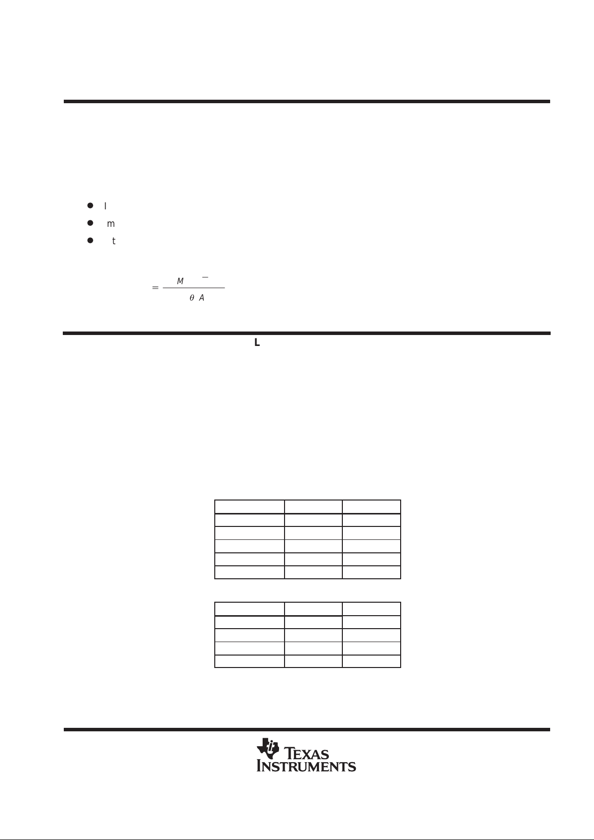
THERMAL INFORMATION
The implementation of integrated circuits in low-profile and fine-pitch surface-mount packages requires special
attention to power dissipation. Many system-dependent issues such as thermal coupling, airflow, added heat
sinks and convection surfaces, and the presence of other heat-generating components affect the powerdissipation limits of a given component.
Three basic approaches for enhancing thermal performance are listed below.
D
Improving the power dissipation capability of the printed-circuit board design
D
Improving the thermal coupling of the component to the printed-circuit board
D
Introducing airflow into the system
Using the given R
θJA
for this device, the maximum power dissipation can be calculated with the equation:
P
D(MAX
)
+
T
J(MAX
)
*
T
A
R
q
JA
APPLICATION INFORMATION
capacitor selection
The output bypass capacitor of each LDO regulator should be selected from the list of ceramic capacitors shown
below. The VCC bypass capacitors should be selected from the list of tantalum capacitors shown below.
T antalum capacitors have good temperature stability and of fer good capacitance for their size. Care should be
taken when using marginal quality tantalum capacitors, as the increase of the equivalent series resistance
(ESR) at low temperatures can cause instability . For a given capacitance, ceramic capacitors are usually larger
and more costly than tantalums. The capacitance of ceramic capacitors varies greatly with temperature. In
addition, the ESR of ceramic capacitors can be low enough to cause instability. A low-value resistor can be
added in series with the ceramic capacitor to provide a minimum ESR.
ceramic (X7R or X5R)
CAPACITANCE CASE SIZE ESR (MAX)
1 µF 0805 3.8 mΩ
2.2 µF 0805 4.5 mΩ
3.3 µF 0805 4.1 mΩ
2.2 µF 1206 3.4 mΩ
4.7 µF 1206 1.9 mΩ
tantalum (6.3 V rating)
CAPACITANCE CASE SIZE ESR (MAX)
4.7 µF A(3216) 6 Ω
6.8 µF A(3216) 6 Ω
10 µF A(3216) 4 Ω
10 µF P(0805) 6 Ω
Page 12

TWL2203
POWER SUPPLY MANAGEMENT IC
SLVS185 – FEBRUAR Y 2000
12
POST OFFICE BOX 655303 • DALLAS, TEXAS 75265
APPLICATION INFORMATION
recommended parts list
REFERENCE DESCRIPTION MANUFACTURER VALUE PART NUMBER
C1 Ceramic, 0805, X7R 100 pF
C2 Ceramic, 0805, X7R 0.01 µF
C3 Tantalum, 6.3 V, Case B, 20% Siemens Matsushita 10 µF B 45 196-E1106-M20
C4 Ceramic, 0805 0.01 µF
C5 Tantalum, 6.3 V, Case B, 20% Siemens Matsushita 10 µF B 45 196-E1106-M20
Cldo1 Ceramic, 0805, X7R 0.22 µF
Cldo2 Ceramic, 10 V , 1206, X5R, 20% Taiyo Yuden 4.7 µF LMK316BJ475ML
Cldo3 Ceramic, 0805, X7R 0.22 µF
Cldo4 Ceramic, 10 V , 1206, X5R, 20% Taiyo Yuden 3.3 µF LMK316BJ335ML
Cldo5 Ceramic, 16 V , 0805, X5R, 20% Taiyo Yuden 2.2 µF LMK212BJ225MG
Cldo6 Ceramic, 10 V , 1206, X5R, 20% Taiyo Yuden 4.7 µF LMK316BJ475ML
Cldo7 Ceramic, 16 V , 0805, X5R, 20% Taiyo Yuden 2.2 µF LMK212BJ225MG
Cvref Ceramic, 0805, X7R 1000 pF
Cdet_delay Ceramic, 0805, X7R 0.1 µF
D1 Schottky diode Rohm RB051L-40
L1 1 µH
M1 Siliconix Si3455DV
Fairchild FDC654P
M2 Siliconix Si3441DV
Siliconix Si3443DV
Siliconix Si2305DS
Fairchild FDC634P
R1 1/4 W, 5% 0.1 Ω
R2 0805, 1/10 W, 5% 10 kΩ
R3 0805, 1/10 W, 5% 1 kΩ
R4 0805, 1/10 W, 5% 560 Ω
R5 0805, 1/10 W, 5% 6.8 kΩ
R6 0805, 1/10 W, 5% 2.7 Ω
R7 0805, 1/10 W, 5% 10 kΩ
Page 13

TWL2203
POWER SUPPLY MANAGEMENT IC
SLVS185 – FEBRUAR Y 2000
13
POST OFFICE BOX 655303 • DALLAS, TEXAS 75265
APPLICATION INFORMATION
battery charging control
M
U
X
R7 R4
R5
R1
C2
C3
M1 M2
D1
C1
R2
4.2 V
Regulation
CVCC
Charge
Switch
Control
Trickle
Charge
Current
Control
Current Limit
Control
+
–
Lithium Ion
Battery
L1
Over-
Voltage
Shutdown
VDET1
VREF
LDO REG 7
VOUT7
Cldo7
EN4
VDET2
VEXT
DET1
VREF
Cvref
Cdet_Delay
DET2
DET_DELAY
C5
C4
Power Switch
EN3
EN2
EN1
LDO REG 1
VOUT1
Cldo1
LDO REG 2
VOUT2
Cldo2
LDO REG 3
VOUT3
Cldo3
LDO REG 4
VOUT4
Cldo4
LDO REG 5
VOUT5
Cldo5
LDO REG 6
VOUT6
Cldo6
Ringer DriveRING
RINGON
MUXOUT
MUXIN0
MUXIN1
MUXIN2
MUXIN3
MUX0
MUX1
_
+
_
+
_
+
VEXT
ENOP_MUX
OP1I+
OP1I–
OP1O
OP12+
OP12–
OP2O
OP12+
OP13–
OP3O
VG1 VCH IADJ ICH+
ICH-
VG2 TCOUT
CH
VB
VSUP
VOUT2
R6
Page 14

TWL2203
POWER SUPPLY MANAGEMENT IC
SLVS185 – FEBRUAR Y 2000
14
POST OFFICE BOX 655303 • DALLAS, TEXAS 75265
APPLICATION INFORMATION
battery-charging control (continued)
The battery-charging control block in the device is a part of the Li-Ion battery charging system of the phone. The
device controls the P-channel MOSFET to accomplish constant-voltage/constant-current charging (CVCC)
within a ±1% tolerance in the charging termination voltage.
The battery charging control consists of the two sections:
D
CVCC charge-switch control with feedback loops for voltage and current control
D
Trickle charge-current control
When the voltage-detector output (DET1) is set high, the voltage-control loop is activated to regulate the voltage
of ICH- to 4.2 V. Then, when the control signal input CH is set high, either the current-control loop or the
trickle-charge control block is activated, depending upon battery voltage.
When VB is below the threshold Vtc, the trickle-charge current control block directs the current to the battery
via TCIN, trickle-charging current control, TCOUT , R6, and the battery . The measure of the voltage across sense
resistor R6 is used for feedback-control of the rate of charging current.
Once the battery voltage reaches the threshold Vtc, the CVCC charge-switch control block becomes active and
controls the P-channel MOSFET M1. The feedback control ensures that the voltage ICH- does not exceed 4.2
V ± 0.05 V (4.2 V regulation), and the current draw of resistor R1 does not exceed the specified value
(current-limit control). In this case, the charging current drains via R1, M2, and the battery. The maximum
charging current is set by external resistors for design flexibility.
analog multiplexer output table
MUX1 MUX2 OUTPUT
0 0 MUXIN0
0 1 MUXIN1
1 0 MUXIN2
1 1 MUXIN3
Page 15
TWL2203
POWER SUPPLY MANAGEMENT IC
SLVS185 – FEBRUAR Y 2000
15
POST OFFICE BOX 655303 • DALLAS, TEXAS 75265
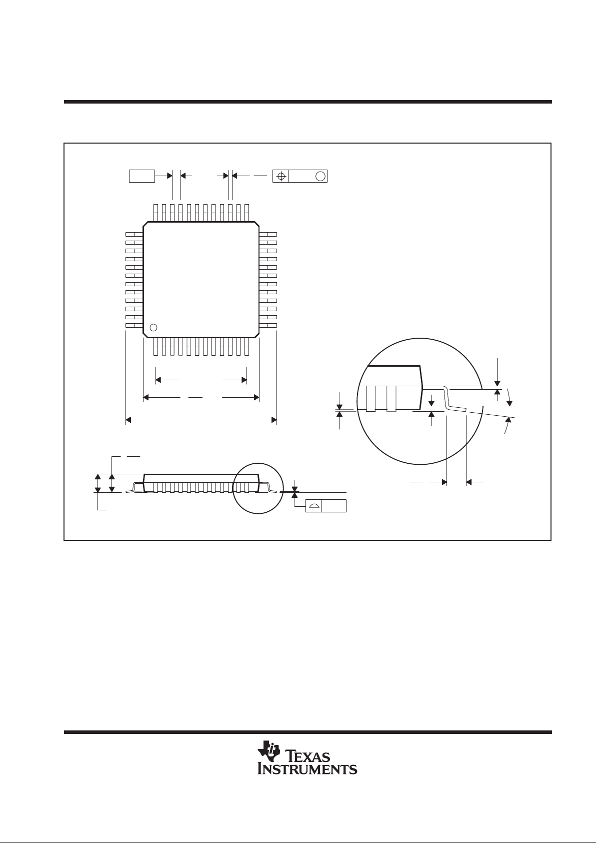
MECHANICAL DATA
PFB (S-PQFP-G48) PLASTIC QUAD FLATPACK
4073176/B 10/96
Gage Plane
0,13 NOM
0,25
0,45
0,75
Seating Plane
0,05 MIN
0,17
0,27
24
25
13
12
SQ
36
37
7,20
6,80
48
1
5,50 TYP
SQ
8,80
9,20
1,05
0,95
1,20 MAX
0,08
0,50
M
0,08
0°–7°
NOTES: A. All linear dimensions are in millimeters.
B. This drawing is subject to change without notice.
C. Falls within JEDEC MS-026
Page 16

IMPORTANT NOTICE
T exas Instruments and its subsidiaries (TI) reserve the right to make changes to their products or to discontinue
any product or service without notice, and advise customers to obtain the latest version of relevant information
to verify, before placing orders, that information being relied on is current and complete. All products are sold
subject to the terms and conditions of sale supplied at the time of order acknowledgement, including those
pertaining to warranty, patent infringement, and limitation of liability.
TI warrants performance of its semiconductor products to the specifications applicable at the time of sale in
accordance with TI’s standard warranty. Testing and other quality control techniques are utilized to the extent
TI deems necessary to support this warranty. Specific testing of all parameters of each device is not necessarily
performed, except those mandated by government requirements.
CERT AIN APPLICATIONS USING SEMICONDUCTOR PRODUCTS MAY INVOL VE POTENTIAL RISKS OF
DEATH, PERSONAL INJURY, OR SEVERE PROPERTY OR ENVIRONMENTAL DAMAGE (“CRITICAL
APPLICATIONS”). TI SEMICONDUCTOR PRODUCTS ARE NOT DESIGNED, AUTHORIZED, OR
WARRANTED TO BE SUITABLE FOR USE IN LIFE-SUPPORT DEVICES OR SYSTEMS OR OTHER
CRITICAL APPLICATIONS. INCLUSION OF TI PRODUCTS IN SUCH APPLICA TIONS IS UNDERSTOOD T O
BE FULLY AT THE CUSTOMER’S RISK.
In order to minimize risks associated with the customer’s applications, adequate design and operating
safeguards must be provided by the customer to minimize inherent or procedural hazards.
TI assumes no liability for applications assistance or customer product design. TI does not warrant or represent
that any license, either express or implied, is granted under any patent right, copyright, mask work right, or other
intellectual property right of TI covering or relating to any combination, machine, or process in which such
semiconductor products or services might be or are used. TI’s publication of information regarding any third
party’s products or services does not constitute TI’s approval, warranty or endorsement thereof.
Copyright 2000, Texas Instruments Incorporated
 Loading...