

Page 1
TWL1110
VOICE-BAND AUDIO PROCESSOR (VBAP)
SLWS103 – NOVEMBER 2000
1
POST OFFICE BOX 655303 • DALLAS, TEXAS 75265
2.7 to 3.3-V Operation
Designed for Analog and Digital Wireless
Handsets and Telecommunications
Applications
Two Differential Microphone Inputs
Differential Earphone Outputs and One
Single-Ended Earphone Output
Earphone and Microphone Mute
Programmable Transmit, Receive, and
Sidetone Paths With Extended Gain and
Attenuation Ranges
Programmable for 15-Bit Linear Data or
8-Bit Companded (µ-law and A-law) Mode
Supports PCM Clock Rates of 128 kHz and
2.048 MHz
Pulse Density Modulated (PDM) Buzzer
Output
On-Chip I
2
C Bus, Which Provides Simple,
Standard, Two-Wire Serial Interface With
Digital ICs
Dual-Tone Multifrequency (DTMF) and
Single-Tone Generator Capable of Up to
8-kHz Tone With Three Selectable
Resolutions of 7.8125 Hz, 15.625 Hz, and
31.25 Hz
2-Channel Auxiliary Multiplexer (MUX)
(Analog Switch)
Capable of Driving 32 Ω Down to a 8-Ω
Speaker
Programmable Power Down Modes
Pin Compatible to TI’s TWL1102, TWL1103,
and TWL1109 Devices for TQFP only
Available in a 32-Pin Thin Quad Flatpack
(TQFP) Package and MicroStar Junior
BGA
description
The TWL1110 provides extended gain and attenuation flexibility for transmit, receive, and sidetone paths. A
differential earphone output is capable of driving speaker loads as low as 8 Ω for use in speaker phone
applications. The single tone function on the TWL1110 generates a single tone output of up to 8 kHz. The
resolution of the DTMF tone is also selectable to 7.8125 Hz, 15.625 Hz, or 31.250 Hz through the interface
control. The analog switch provides more control capabilities for voice-band audio processor (VBAP).
The VBAP is an analog-digital interface for voice band signals designed with a combination of coders and
decoders (codecs) and filters. It is a low-power device with companding options and programming features, and
it meets the requirements for communication systems, including the cellular phone. The device operates in
either the 15-bit linear or 8-bit companded (µ-law or A-Law) mode, which is selectable through the I
2
C interface.
A coder, an analog-to-digital converter or ADC, digitizes the analog voice signal, and a decoder, an
digital-to-analog converter or DAC, analogs the digital-voice signal. VBAP provides a companding option to
overcome the bandwidth limitations of telephone networks without degradation in sound quality. The human
auditory system is a logarithmic system in which high amplitude signals require less resolution than low
amplitude signals. Therefore, an 8-bit code word with nonuniform quantization (µ-law or A-law) has the same
quality as 13-bit linear coding. VBAP provides better digital code words by generating a 15-bit linear coding
option.
This device contains circuits to protect its inputs and outputs against damage due to high static voltages or electrostatic fields. These
circuits have been qualified to protect this device against electrostatic discharges (ESD) of up to 2 kV according to MIL-STD-883C,
Method 3015; however, it is advised that precautions be taken to avoid application of any voltage higher than maximum-rated
voltages to these high-impedance circuits. During storage or handling, the device leads should be shorted together or the device
should be placed in conductive foam. In a circuit, unused inputs should always be connected to an appropriated logic voltage level,
preferably either VCC or ground. Specific guidelines for handling devices of this type are contained in the publication
Guidelines for
Handling Electrostatic-Discharge-Sensitive (ESDS) Devices and Assemblies
available from Texas Instruments.
Please be aware that an important notice concerning availability, standard warranty, and use in critical applications of
Texas Instruments semiconductor products and disclaimers thereto appears at the end of this data sheet.
†
These options are available on some devices. Please see the table of comparison for the last two generations of VBAPs.
Copyright 2000, Texas Instruments Incorporated
MicroStar Junior and VBAP are trademarks of Texas Instruments.
All other trademarks are the property of their respective owners.
PRODUCTION DATA information is current as of publication date.
Products conform to specifications per the terms of Texas Instruments
standard warranty. Production processing does not necessarily include
testing of all parameters.
Page 2

TWL1110
VOICE-BAND AUDIO PROCESSOR (VBAP)
SLWS103 – NOVEMBER 2000
2
POST OFFICE BOX 655303 • DALLAS, TEXAS 75265
description (continued)
The human voice is effective from a frequency range of 300 Hz to 3300 Hz in telephony applications. In order
to eliminate unwanted signals, the VBAP design has two types of filters that operate in both the transmit and
receive path. A low-pass filter attenuates the signals over 4 kHz. A selectable high-pass filter cleans up the
signals under 100 Hz. This reduces noise that may have coupled in from 50/60-Hz power cables. The high-pass
filter is bypassed by selecting the corresponding register bit.
VBAP has many programming features that are controlled using a 2-wire standard serial I
2
C interface. This
allows the device to interface with many digital ICs such as a DSP or a microprocessor. The device has seven
registers: power control, mode control, transmit PGA, receive PGA, high DTMF , low DTMF, and auxiliary mode
control. Some of the programmable features that can be controlled by I2C interface include:
Transmit amplifier gain
Receive amplifier gain
Sidetone gain
Volume control
Earphone control
PLL power control
Microphone selection
Transmit channel high-pass filter control
Receive channel high-pass filter control
Companding options and selection control
PCM loopback
DTMF control
Pulse density modulated control
The VBAP is also capable of generating its own internal clocks from a 2.048-MHz master clock input.
Page 3
TWL1110
VOICE-BAND AUDIO PROCESSOR (VBAP)
SLWS103 – NOVEMBER 2000
3
POST OFFICE BOX 655303 • DALLAS, TEXAS 75265
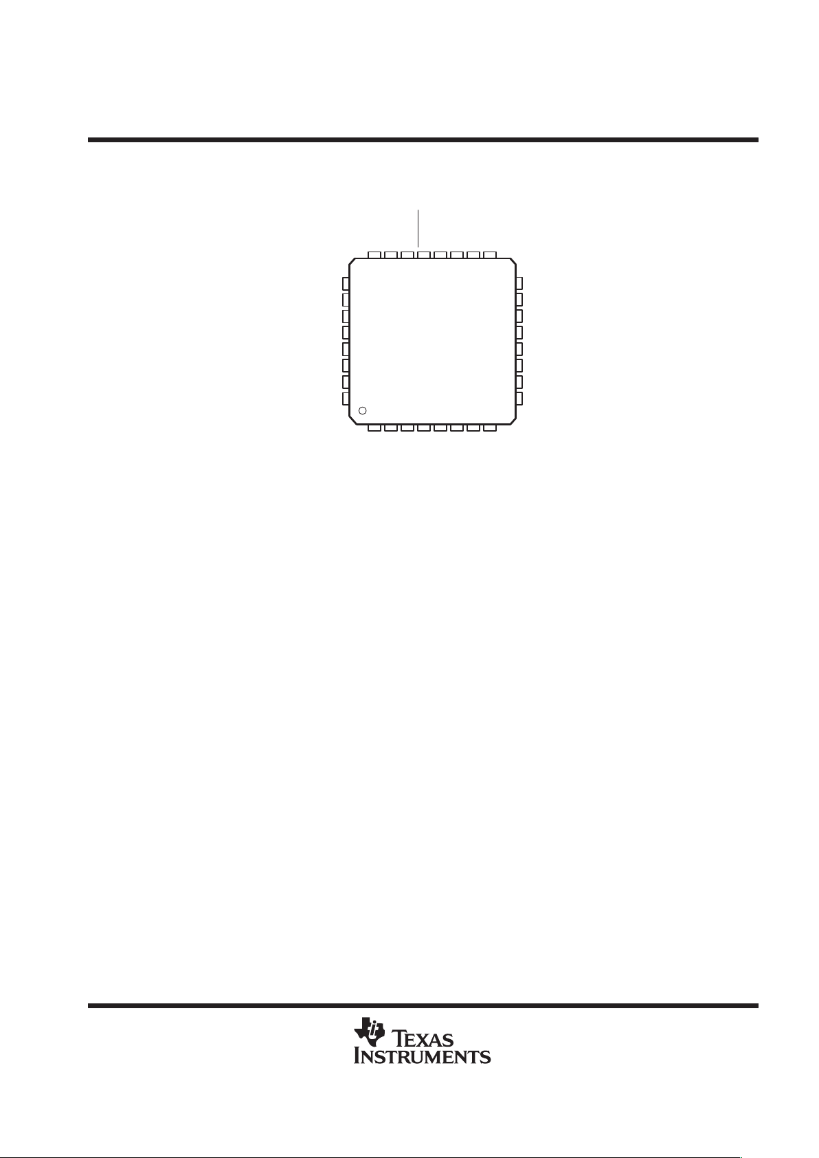
PBS PACKAGE
(TOP VIEW)
31
30
29
28
27
9
10
PCMO
PCMI
DV
SS
DV
DD
SCL
SDA
MUXOUT2
MUXOUT1
PLLV
DD
EARV
SS
EAR1ON
EARV
DD
EAR1OP
EARV
SS
EAR2O
AV
DD
32
26
11
12
13
14
15
MBIAS
MIC1P
MIC1N
MIC2P
MUXIN
16
25
1234567 8
24 23 22 21 20 19 18 17
MIC2N
REXT
AV
SS
MCLK
PLLV
SS
V
SS
RESET
PWRUPSEL
BUZZCON
PCMSYN
PCMCLK
Page 4
TWL1110
VOICE-BAND AUDIO PROCESSOR (VBAP)
SLWS103 – NOVEMBER 2000
4
POST OFFICE BOX 655303 • DALLAS, TEXAS 75265
functional block diagram
PCMIN
PCMSYN
PCMCLK
MIC1P
MIC1N
MIC2P
MIC2N
MIC
Amplifier
1
g =
23.5 dB
MIC
Amplifier
2
g = 6
or
18 dB
Analog
Modulator
TX Filter
and PGA
g = –10 dB
to
0 dB
PCM
Interface
Sidetone
g = –24 db
to
–12 dB
RX Vol
Control
g = –18 dB
to
0 dB
RX Filter
and PGA
g = – 6 dB
to
+6 dB
Digital
Modulator
and Filter
Ear
Amp1
Ear
Amp2
DTMF
Generator
Control Bus
REF PLL
Buzzer
Control
Power and RESET
SCLK
SDATA
MBIAS
REXT
MCLK
RESET
SS
EARV
DD
EARV
SS
PLLV
DD
PLLV
SS
DV
DD
DV
SS
AV
DD
AV
SS
V
PWRUPSEL
PCMOUT
EAR1OP
EAR1ON
EAR2O
BUZZCON
DTMF
GAIN
DTMF
Voice
0 dBor6 dB
MUX
–12 to
12 dB
in 6dB
Steps
I C
MUX
IN
OUT
OUT
I/F
2
Page 5

TWL1110
VOICE-BAND AUDIO PROCESSOR (VBAP)
SLWS103 – NOVEMBER 2000
5
POST OFFICE BOX 655303 • DALLAS, TEXAS 75265
functional description
power on/reset
The power for the various digital and analog circuits is separated to improve the noise performance of the
device. An external reset must be applied to the active low/RESET terminal to guarantee reset upon power on
and to bring the device to an operational state. After the initial power-on sequence the device can be functionally
powered up and powered down by writing to the power control register through the I
2
C interface. The device
has a pin-selectable power up in the default mode option. The hardwired pin-selectable PWRUPSEL function
allows the VBAP to power up in the default mode and to be used without a microcontroller.
reference
A precision band gap reference voltage is generated internally and supplies all required voltage references to
operate the transmit and receive channels. The reference system also supplies bias voltage for use with an
electret microphone at terminal MBIAS. An external precision resistor is required for reference current setting
at terminal REXT.
I2C control interface
The I
2
C interface is a two-wire bidirectional serial interface. The I2C interface controls the VBAP by writing data
to seven control registers:
Power control
Mode control
Transmit PGA and sidetone control
Receive PGA gain and volume control
DTMF routing
Tone selection control
Auxiliary control
There are two power up modes which may be selected at the PWRUPSEL terminal: (1) The PWRUPSEL state
(VDD at terminal 20) causes the device to power up in the default mode when power is applied. Without an I2C
interface or controlling device, the programmable functions are fixed at the default gain levels, and functions
such as the sidetone and DTMF are not accessible. (2) The PWRUPSEL state (ground at terminal 20) causes
the device to go to a power down state when power is applied. In this mode an I
2
C interface is required to power
up the device.
phase-locked loop (PLL)
The phase-lock loop generates the internal clock frequency required for digital filters and modulators by phase
locking to 2.048 MHz master clock input.
PCM interface
The PCM interface transmits and receives data at the PCMO and PCMI terminals respectively. The data is
transmitted or received at the PCMCLK speed once every PCMSYN cycle. The PCMCLK can be tied directly
to the 128-kHz or 2.048-MHz master clock (MCLK). The PCMSYN can be driven by an external source or
derived from the master clock and used as an interrupt to the host controller.
microphone amplifiers
The microphone input is a switchable interface for two differential microphone inputs. The first stage is a
low-noise differential amplifier that provides a gain of 23.5 dB. The second-stage amplifier has a selectable gain
of 6 or 18 dB.
Page 6

TWL1110
VOICE-BAND AUDIO PROCESSOR (VBAP)
SLWS103 – NOVEMBER 2000
6
POST OFFICE BOX 655303 • DALLAS, TEXAS 75265
functional description (continued)
analog modulator
The transmit channel modulator is a third-order sigma-delta design.
transmit filter and PGA
The transmit filter is a digital filter designed to meet CCITT G.714 requirements. The device operates either in
the 15-bit linear or 8-bit companded µ-law or in the A-law mode, which is selectable through the I
2
C interface.
The transmit PGA defaults to 0 dB.
sidetone
A portion of the transmitted audio is attenuated and fed back to the receive channel through the sidetone path.
The sidetone path defaults to the mute condition. The default gain of -12 dB is set in the sidetone control register.
The sidetone path can be enabled by writing to the power control register.
receive volume control
The receive volume control block acts as an attenuator with a range of –18 dB to 0 dB in 2-dB steps for control
of the receive channel volume. The receive volume control gain defaults to 0 dB.
receive filter and PGA
The receive filter is a digital filter that meets CCITT G.714 requirements with a high-pass filter that is selectable
through the I2C interface. The device operates either in the 15-bit linear or the 8-bit µ-law or the A-law
companded mode, which is selectable through the I2C interface. The gain defaults to –4 dB, representing a
3-dBm level for a 32-Ω load impedance and the corresponding digital full scale PCMI code.
digital modulator and filter
The second-order digital modulator and filter convert the received digital PCM data to the analog output required
by the earphone interface.
earphone amplifiers
The analog signal can be routed to either of two earphone amplifiers, one with differential output (EAR1ON and
EAR1OP) and one with single-ended output (EAR2O). Clicks and pops are suppressed for EAR1 differential
output only.
tone generator
The tone generator provides generation of standard DTMF tones which are output to (1) the buzzer driver, as
a PDM signal, (2) the receive path DAC for outputting through the earphone, or (3) as PCMO data. The integer
value is loaded into one of two 8-bit registers, the high-tone register (04), or the low-tone register (05) (see the
Register Map Addressing
section). The tone output is 2 dB higher when applied to the high tone register (04).
The high DTMF tones must be applied to the high-tone register, and the low DTMF tones to the low-tone register .
The tone signals can be generated with 3 different resolutions at ∆F= 7.8125 Hz, 15.625 Hz, and 31.250 Hz.
The resolution option can be selected by setting the register (06).
analog mux
The analog switch can be used to source an analog signal to two different loads. The output can be reselected
by setting the auxiliary register (06).
Page 7
TWL1110
VOICE-BAND AUDIO PROCESSOR (VBAP)
SLWS103 – NOVEMBER 2000
7
POST OFFICE BOX 655303 • DALLAS, TEXAS 75265
functional description (continued)
DTMF gain MUX
The DTMF gain MUX selects the signal path and applies the appropriate gain setting. Therefore the device is
either in tone mode or in voice mode. When set in the voice mode, the gain is controlled by the auxiliary register
and is set to 0 dB or 6 dB. When set in the tone mode, the gain is from –12 dB to 12 dB in 6-dB steps which
is set by the volume control register. The gain setting is controlled by the RXPGA register. This will not create
any control contention since the device is working in one mode at a time.
Terminal Functions
TERMINAL
†
NO.
I/O DESCRIPTION
NAME
µBGA TQFP
I/O
DESCRIPTION
AV
DD
A1 32 I Analog positive power supply
AV
SS
J1 8 I Analog negative power supply (use for ground connection)
BUZZCON F9 19 O Buzzer output, a pulse-density modulated signal to apply to external buzzer driver
DV
DD
J6 13 I Digital positive power supply
DV
SS
J7 14 I Digital negative power supply
EAR1ON A6 27 O Earphone 1 amplifier output (–)
EAR1OP A4 29 O Earphone 1 amplifier output (+)
EAR2O A2 31 O Earphone 2 amplifier output
EARV
DD
A5 28 I Analog positive power supply for the earphone amplifiers
EARV
SS
A3, A7 30, 26 I Analog negative power supply for the earphone amplifiers
MBIAS B1 1 O Microphone bias supply output, no decoupling capacitors
MCLK C9 22 I Master system clock input (2.048 MHz, digital)
MIC1P C1 2 I MIC1 input (+)
MIC1N D1 3 I MIC1 input (–)
MIC2P E1 4 I MIC2 input (+)
MIC2N F1 5 I MIC2 input (–)
MUXIN H1 7 I Analog MUX input
MUXOUT1 J2 9 I Analog MUX output
MUXOUT2 J3 10 I Analog MUX output
PCMI J8 15 I Receive PCM input
PCMO J9 16 O Transmit PCM output
PCMSYN G9 18 I PCM frame sync
PCMCLK H9 17 I PCM data clock
PLLV
SS
A9 24 I PLL negative power supply
PLLV
DD
A8 25 I PLL digital power supply
PWRUPSEL E9 20 I Selects the power-up default mode
REXT G1 6 I/O Internal reference current setting terminal (use precision 100-kΩ resistor and no filtering
capacitors)
RESET D9 21 I Active low reset
SCL J5 12 I I2C-bus serial clock (this input is used to synchronize the data transfer from and to the
VBAP)
SDA J4 11 I/O I2C-bus serial address/data input/output. This is a bidirectional terminal used to transfer
register control addresses and data into and out of the codec. It is an open
-drain terminal
and therefore requires a pullup resistor to VDD (typical 10 kΩ for 100 kHz).
V
SS
B9 23 I Ground return for bandgap internal reference (use for ground connection)
†
All MicroStar Junior BGA pins that are not mentioned have no internal connection.
Page 8
TWL1110
VOICE-BAND AUDIO PROCESSOR (VBAP)
SLWS103 – NOVEMBER 2000
8
POST OFFICE BOX 655303 • DALLAS, TEXAS 75265
absolute maximum ratings over operating free-air temperature range (unless otherwise noted)
†
Supply voltage range –0.5 V to 3.6 V. . . . . . . . . . . . . . . . . . . . . . . . . . . . . . . . . . . . . . . . . . . . . . . . . . . . . . . . . . . . . .
Output voltage range –0.5 V to 3.6 V. . . . . . . . . . . . . . . . . . . . . . . . . . . . . . . . . . . . . . . . . . . . . . . . . . . . . . . . . . . . . .
Input voltage range –0.5 V to 3.6 V. . . . . . . . . . . . . . . . . . . . . . . . . . . . . . . . . . . . . . . . . . . . . . . . . . . . . . . . . . . . . . . .
Continuous total power dissipation See Dissipation Rating Table. . . . . . . . . . . . . . . . . . . . . . . . . . . . . . . . . . . . . .
Operating free air temperature range (industrial temperature) –40°C to 85°C. . . . . . . . . . . . . . . . . . . . . . . . . . .
Storage temperature range, testing –65°C to 150°C. . . . . . . . . . . . . . . . . . . . . . . . . . . . . . . . . . . . . . . . . . . . . . . . .
Lead temperature 1,6 mm from case for 10 seconds 260°C. . . . . . . . . . . . . . . . . . . . . . . . . . . . . . . . . . . . . . . . . .
†
Stresses beyond those listed under “absolute maximum ratings” may cause permanent damage to the device. These are stress ratings only, and
functional operation of the device at these or any other conditions beyond those indicated under “recommended operating conditions” is not
implied. Exposure to absolute-maximum-rated conditions for extended periods may affect device reliability.
DISSIPATION RATING TABLE
PACKAGE
TA ≤ 25°C
POWER RATING
DERATING FACTOR
ABOVE TA = 25°C
TA = 85°C
POWER RATING
COMMENTS
TQFP 702 mW 7.2 mW/°C 270 mW low dissipation printed
circuit board (PCB)
MicroStar Junior BGA 660 mW 164 mW/°C 220 mW low dissipation PCB
MicroStar Junior BGA 2.75 W 36 mW/°C 917 mW high dissipation PCB
recommended operating conditions (see Notes 1 and 2)
MIN NOM MAX UNIT
Supply voltage, AVDD, DVDD, PLLVDD, EARV
DD
2.7 3.3 V
High-level input voltage (V
IHMIN
) 0.7xV
DD
V
Low-level input voltage (V
ILMAX
) 0.3xV
DD
V
Load impedance between EAR1OP and EAR1ON-R
L
8 to 32 Ω
Load impedance for EAR2OP-R
L
32 Ω
Operating free-air temperature, T
A
–40 85 C
NOTES: 1. To avoid possible damage and resulting reliability problems to these CMOS devices, follow the power on initialization paragraph,
described in the
Principles of Operation
.
2. Voltages are with respect to AVSS, DV
SS,
PLLVSS,
and
EARV
SS.
electrical characteristics over recommended ranges of supply voltage and free-air temperature (unless
otherwise noted)
supply current
PARAMETER TEST CONDITIONS MIN TYP MAX UNIT
Operating, EAR1 selected, MicBias disabled 4.5 6 mA
Operating, EAR2 selected, MicBias disabled 4.5 6 mA
I Supply current from V
DD
Power down room temperature, VDD = 3.0 V, Reg 6 bit 7 =
1, MClk not present (see Note 3)
2 10 µA
Power down room temperature, VDD = 3.0 V, , Reg 6 bit 7 =
0, MClk not present (see Note 3)
10 30 µA
t
on(i)
Power-up time from power down 5 10 ms
3. V
IHMIN
= V
DD, VILMAX
= V
SS.
Page 9
TWL1110
VOICE-BAND AUDIO PROCESSOR (VBAP)
SLWS103 – NOVEMBER 2000
9
POST OFFICE BOX 655303 • DALLAS, TEXAS 75265
electrical characteristics over recommended ranges of supply voltage and free-air temperature (unless
otherwise noted) (continued)
digital interface
PARAMETER TEST CONDITIONS MIN TYP MAX UNIT
V
OH
High-level output voltage PCMO (BuzzCon) IOH = –3.2 mA, VDD = 3 V DVDD –0.25 V
V
OL
Low-level output voltage PCMO IOL = 3.2 mA, VDD = 3 V 0.25 V
I
IH
High-level input current, any digital input VI = V
DD
10 µA
I
IL
Low-level input current, any digital input VI = V
SS
10 µA
C
I
Input capacitance 10 pF
C
O
Output capacitance 20 pF
R
L
Load impedance (BuzzCon) 5 kΩ
0
5
10
15
20
25
30
35
40
45
–50 0 50 100
0
5
10
15
20
25
30
–50 0 50 100
SUPPLY CURRENT
vs
FREE AIR TEMPERATURE
(Detector OFF)
SUPPLY CURRENT
vs
FREE AIR TEMPERATURE
(Detector ON)
DD
I Supply Current – –Aµ
DD
I Supply Current – –Aµ
TA – Free-Air Temperature – °CT
A
– Free-Air Temperature – °C
VDD = 3.3 V
VDD = 3.0 V
VDD = 3.3 V
VDD = 3.0 V
VDD = 2.7 V
VDD = 2.7 V
microphone interface
PARAMETER TEST CONDITIONS MIN TYP MAX UNIT
V
IO
Input offset voltage at MIC1N, MIC2N See Note 4 –5 5 mV
I
IB
Input bias current at MIC1N, MIC2N –300 300 nA
C
i
Input capacitance at MIC1N, MIC2N 5 pF
V
n
Microphone input referred noise, psophometrically weighted,
(C-message weighted is similar)
MIC Amp 1 gain = 23.5 dB
MIC Amp 2 gain = 0 dB
3 4.7 µV
rms
IOmax Output source current – MBIAS 1 1.2 mA
V
(mbias)
Microphone bias supply voltage (see Note 5) 2.3 2.5 2.65 V
MICMUTE –80 dB
Input impedance Fully differential 35 60 100 kΩ
NOTES: 4. Measured while MIC1P and MIC1N are connected together. Less than 0.5-mV offset results in 0 value code on PCMOUT.
5. Not a JEDEC symbol.
Page 10
TWL1110
VOICE-BAND AUDIO PROCESSOR (VBAP)
SLWS103 – NOVEMBER 2000
10
POST OFFICE BOX 655303 • DALLAS, TEXAS 75265
electrical characteristics over recommended ranges of supply voltage and free-air temperature (unless
otherwise noted) (continued)
speaker interface
PARAMETER TEST CONDITIONS MIN TYP MAX UNIT
VDD = 2.7 V , fully differential, 8-Ω load,
3-dBm0 output, volume control = –3 dB,
RXPGA = –4 dB level
161 200
Earphone AMP1 output power (see Note 6)
VDD = 2.7 V , fully differential, 16-Ω load,
3-dBm0 output, volume control = –3 dB,
RXPGA = –2 dB level
128 160
mW
VDD = 2.7 V , fully differential, 32-Ω load,
3-dBm0 output, volume control = –3 dB,
RXPGA = –1 dB level
81 100
Earphone AMP2 output power (see Note 6)
VDD = 2.7 V, single-ended, 32-Ω load,
3-dBm0 output
10 12.5 mW
V
OO
Output offset voltage at EAR1 Fully differential ±5 ±30 mV
3-dBm0 input, 8-Ω load 141 178
Maximum output current for EAR1 (rms)
3-dBm0 input, 16-Ω load
90 112
IOmax
Maximum out ut current for EAR1 (rms)
3-dBm0 input, 32-Ω load 50 63
mA
Maximum output current for EAR2 (rms) 3-dBm0 input 17.7 22.1
EARMUTE –80 dB
NOTE 6: Maximum power is with a load impedance of –25%.
transmit gain and dynamic range, companded mode (µ-law or A-law) or linear mode selected, transmit slope
filter bypassed (see Notes 7 and 8)
PARAMETER TEST CONDITIONS MIN TYP MAX UNIT
Transmit reference-signal level (0 dB) Differential 87.5 mV
pp
Differential, normal mode 124
Overload-signal level (3 dBm0)
Differential, extended mode 31.5
mV
pp
Absolute gain error 0 dBm0 input signal, VDD ±10% –1 1 dB
MIC1N, MIC1P to PCMO at 3 dBm0 to –30 dBm0 –0.5 0.5
Gain error with input level relative to gain at
–
MIC1N, MIC1P to PCMO at –31 dBm0 to –45 dBm0 –1 1
dB
–10 dBm0
MIC1N, MIC1P to PCMO
MIC1N, MIC1P to PCMO at –46 dBm0 to –55 dBm0 –1.2 1.2
dB
NOTES: 7. Unless otherwise noted, the analog input is 0 dB, 1020-Hz sine wave, where 0 dB is defined as the zero-reference point of the channel
under test.
8. The reference signal level, which is input to the transmit channel, is defined as a value 3 dB below the full-scale value of 88-mV
rms
.
transmit gain and dynamic range, companded mode (µ-law or A-law) or linear mode selected, transmit slope
filter enabled (see Notes 7 and 8)
PARAMETER TEST CONDITIONS MIN TYP MAX UNIT
Transmit reference-signal level (0 dB) Differential 87.5 mV
pp
Differential, normal mode 124 mV
pp
Overload-signal level (3 dBm0)
Differential, extended mode 31.5 mV
pp
Absolute gain error 0 dBm0 input signal, VDD ±10% –1 1 dB
MIC1N, MIC1P to PCMO at 3 dBm0 to –30 dBm0 –0.5 0.5
Gain error with input level relative to gain at
–
MIC1N, MIC1P to PCMO at –31 dBm0 to –45 dBm0 –1 1
dB
–10 dBm0
MIC1N, MIC1P to PCMO
MIC1N, MIC1P to PCMO at –46 dBm0 to –55 dBm0 –1.2 1.2
dB
NOTES: 7. Unless otherwise noted, the analog input is 0 dB, 1020-Hz sine wave, where 0 dB is defined as the zero-reference point of the
channel under test.
8 The reference signal level, which is input to the transmit channel, is defined as a value 3 dB below the full-scale value of 88-mV
rms
.
Page 11
TWL1110
VOICE-BAND AUDIO PROCESSOR (VBAP)
SLWS103 – NOVEMBER 2000
11
POST OFFICE BOX 655303 • DALLAS, TEXAS 75265
electrical characteristics over recommended ranges of supply voltage and free-air temperature (unless
otherwise noted) (continued)
transmit filter transfer, companded mode (µ-law or A-law) or linear mode selected, transmit slope filter
bypassed (MCLK = 2.048 MHz)
PARAMETER TEST CONDITIONS MIN TYP MAX UNIT
f
MIC1
or f
MIC2
<100 Hz –0.5 0.5
f
MIC1
or f
MIC2
= 200 Hz –0.5 0.5
f
MIC1
or f
MIC2
= 300 Hz to 3 kHz –0.5 0.5
Gain relative to input signal gain at 1020 Hz, internal high-pass
f
MIC1
or f
MIC2
= 3.4 kHz –1.5 0
dB
filt
er disable
d
f
MIC1
or f
MIC2
= 4 kHz –14
dB
f
MIC1
or f
MIC2
= 4.6 kHz –35
f
MIC1
or f
MIC2
= 8 k Hz –47
Gain relative to input signal gain at 1020 Hz, internal high-pass
f
MIC1
or f
MIC2
<100 Hz –15
Gain relative to in ut signal gain at 1020 Hz, internal high ass
filter enabled
f
MIC1
or f
MIC2
= 200 Hz –5
dB
transmit filter transfer, companded mode (µ-law or A-law) or linear mode selected, transmit slope filter
selected, transmit high-pass filter enabled (MCLK = 2.048 MHz) (see Note 9)
PARAMETER TEST CONDITIONS MIN TYP MAX UNIT
f
MIC1
or f
MIC2
=100 Hz –27 dB
f
MIC1
or f
MIC2
= 200 Hz –8 dB
f
MIC1
or f
MIC2
= 250 Hz –4 dB
f
MIC1
or f
MIC2
= 300 Hz –1.80 dB
f
MIC1
or f
MIC2
= 400 Hz –1.50 dB
f
MIC1
or f
MIC2
= 500 Hz –1.30 dB
f
MIC1
or f
MIC2
= 600 Hz –1.1 dB
f
MIC1
or f
MIC2
= 700 Hz –0.8 dB
f
MIC1
or f
MIC2
= 800 Hz –0.57 dB
f
MIC1
or f
MIC2
= 900 Hz –0.25 dB
f
MIC1
or f
MIC2
= 1000 Hz 0 dB
Gain relative to input signal gain at 1.02 kHz, with slope filter selected
f
MIC1
or f
MIC2
= 1500 Hz 1.8 dB
f
MIC1
or f
MIC2
= 2000 Hz 4.0 dB
f
MIC1
or f
MIC2
= 2500 Hz 6.5 dB
f
MIC1
or f
MIC2
= 3000 Hz 7.6 dB
f
MIC1
or f
MIC2
= 3100 Hz 7.7 dB
f
MIC1
or f
MIC2
= 3300 Hz 8.0 dB
f
MIC1
or f
MIC2
= 3500 Hz 6.48 dB
f
MIC1
or f
MIC2
= 4000 Hz –13 dB
f
MIC1
or f
MIC2
= 4500 Hz –35 dB
f
MIC1
or f
MIC2
= 5000 Hz –45 dB
f
MIC1
or f
MIC2
= 8000 Hz –50 dB
NOTE 9: The pass-band tolerance is ±0.25 dB from 300 Hz to 3500 Hz.
Page 12
TWL1110
VOICE-BAND AUDIO PROCESSOR (VBAP)
SLWS103 – NOVEMBER 2000
12
POST OFFICE BOX 655303 • DALLAS, TEXAS 75265
electrical characteristics over recommended ranges of supply voltage and free-air temperature (unless
otherwise noted) (continued)
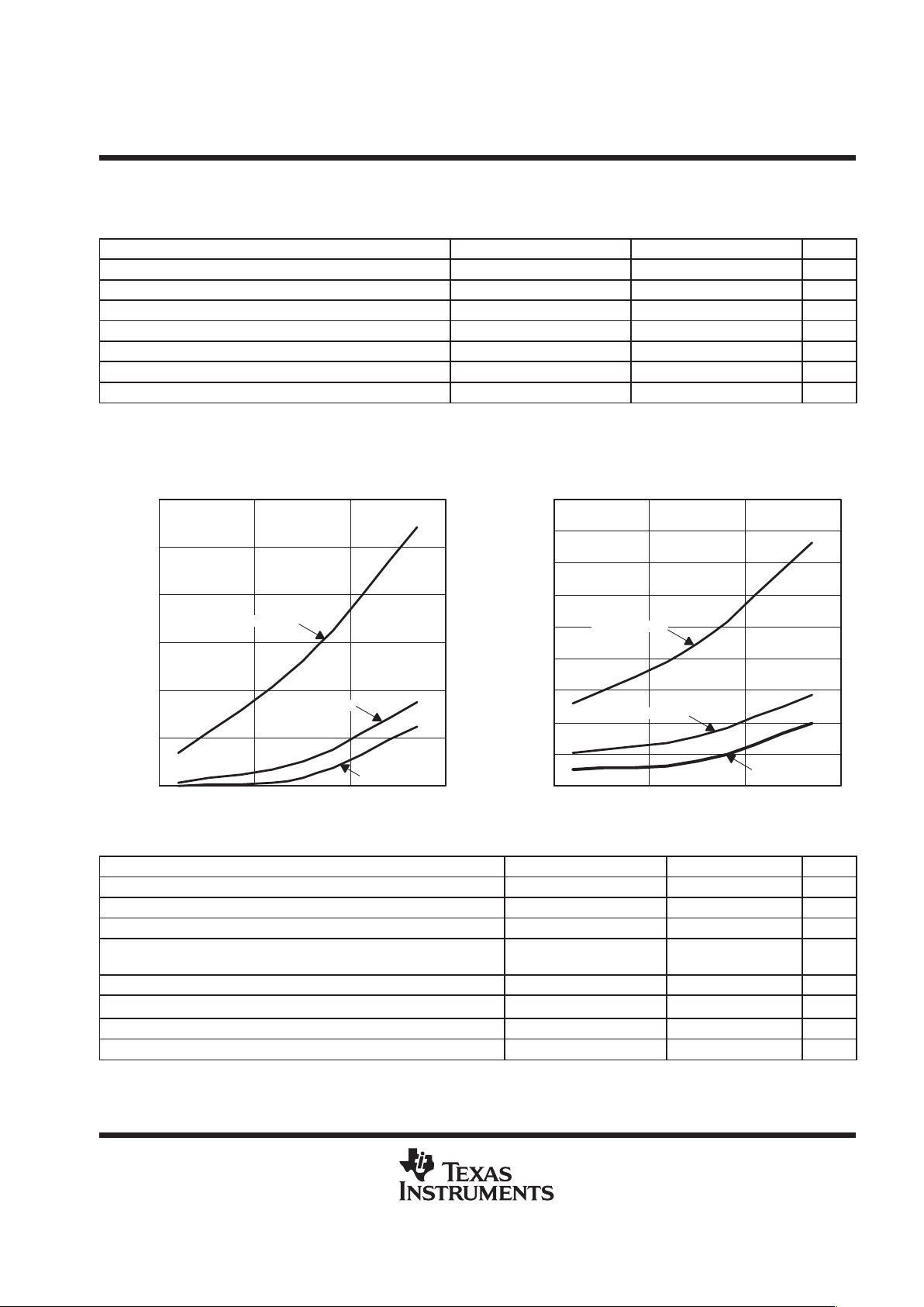
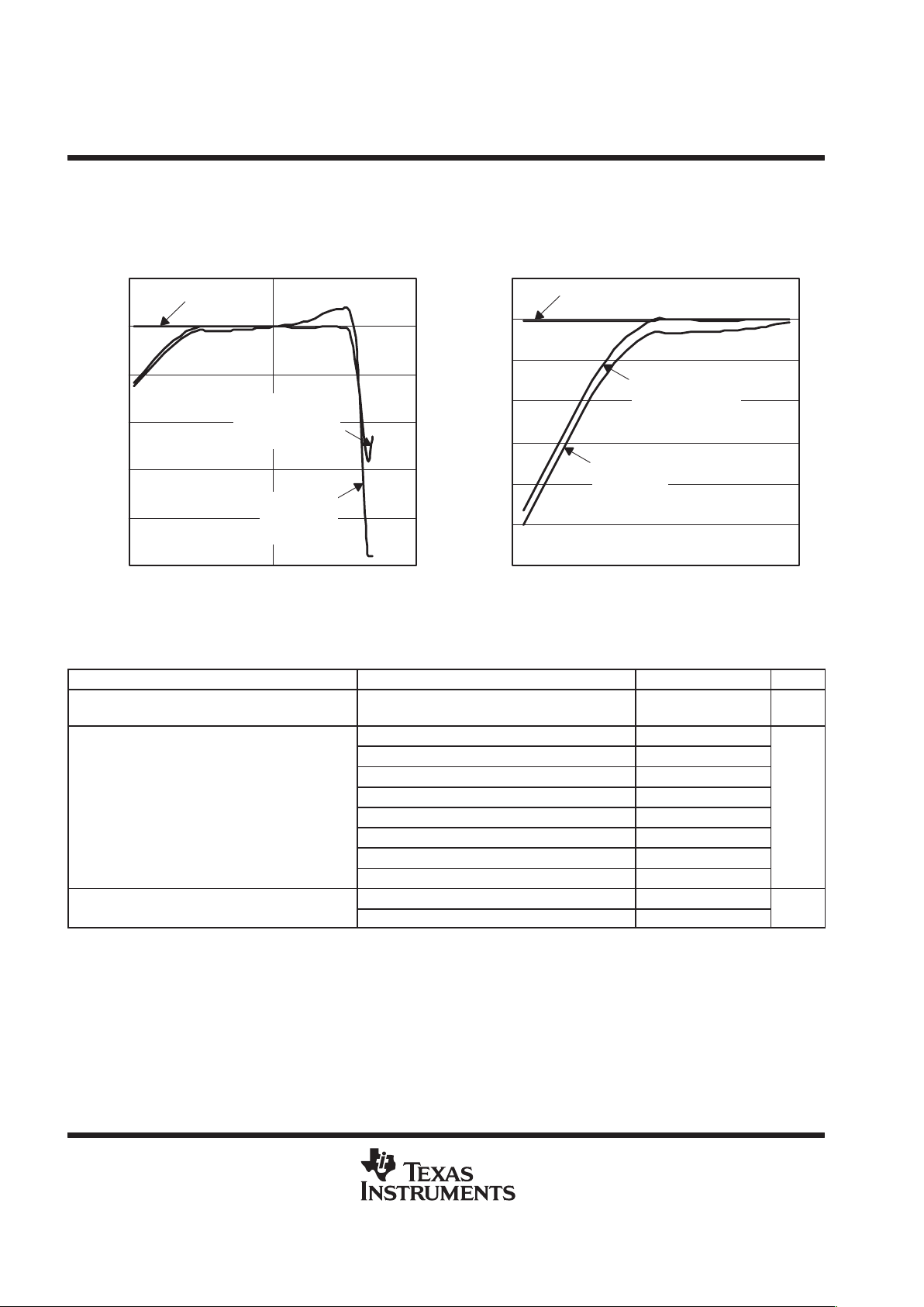
–30
–25
–20
–15
–10
–5
0
5
100 1000
Relative Gain – dB
–100
–80
–60
–40
–20
0
20
100 1000 10000
Relative Gain – dB
RELATIVE GAIN
vs
FREQUENCY
RELATIVE GAIN
vs
FREQUENCY
f – Frequency – Hz f – Frequency – Hz
Both Filters
Disabled
High Pass
Filter and
Slope Filter
Selected
High Pass
Filter Selected
and Slope Filter
Disabled
Both Filters
Disabled
High Pass
Filter Selected
and Slope Filter
Disabled
High Pass
Filter and
Slope Filter
Selected
Figure 1. Transmit Gain Response With Respect to Gain of 1 kHz Tone
transmit idle channel noise and distortion, companded mode (µ-law or A-law) selected, slope filter bypassed
PARAMETER TEST CONDITIONS MIN TYP MAX UNIT
Transmit idle channel noise, psophometrically
weighted
TXPGA gain= 0 dB, MIC Amp 1 gain = 23.5 dB,
MIC Amp 2 gain = 6 dB
–83.5 –78 dBm0
p
MIC1N, MIC1P to PCMO at 3 dBm0 27
MIC1N, MIC1P to PCMO at 0 dBm0 30
MIC1N, MIC1P to PCMO at –5 dBm0 33
Transmit signal-to-distortion ratio with
MIC1N, MIC1P to PCMO at –10 dBm0 36
Transmit signal to distortion ratio with
1020-Hz sine-wave input
MIC1N, MIC1P to PCMO at –20 dBm0 35
dBm0
MIC1N, MIC1P to PCMO at – 30 dBm0 26
MIC1N, MIC1P to PCMO at – 40 dBm0 24
MIC1N, MIC1P to PCMO at – 45 dBm0 19
Intermodulation distortion, 2-tone CCITT method,
CCITT G.712 (7.1), R2 49
Intermodulation distortion, 2 tone CCITT method
,
composite power level, –13 dBm0
CCITT G.712 (7.2), R2 51
dB
Page 13

TWL1110
VOICE-BAND AUDIO PROCESSOR (VBAP)
SLWS103 – NOVEMBER 2000
13
POST OFFICE BOX 655303 • DALLAS, TEXAS 75265
electrical characteristics over recommended ranges of supply voltage and free-air temperature (unless
otherwise noted) (continued)
transmit idle channel noise and distortion, companded mode (µ-law or A-law) selected, slope filter enabled
PARAMETER TEST CONDITIONS MIN TYP MAX UNIT
Transmit idle channel noise, psophometrically
weighted
TXPGA gain= 0 dB, MIC Amp 1 gain = 23.5 dB,
MIC Amp 2 gain = 6 dB
–83.5 –78 dBm0
p
MIC1N, MIC1P to PCMO at 3 dBm0 27
MIC1N, MIC1P to PCMO at 0 dBm0 30
MIC1N, MIC1P to PCMO at –5 dBm0 33
Transmit signal-to-total distortion ratio with 1020-Hz
MIC1N, MIC1P to PCMO at –10 dBm0 36
Transmit signal to total distortion ratio with 1020 Hz
sine-wave input
MIC1N, MIC1P to PCMO at –20 dBm0 35
dBm0
MIC1N, MIC1P to PCMO at –30 dBm0 26
MIC1N, MIC1P to PCMO at –40 dBm0 24
MIC1N, MIC1P to PCMO at –45 dBm0 19
Intermodulation distortion, 2-tone CCITT method,
CCITT G.712 (7.1), R2 49
Intermodulation distortion, 2 tone CCITT method
,
composite power level, –13 dBm0
CCITT G.712 (7.2), R2 51
dB
transmit idle channel noise and distortion, linear mode selected, slope filter bypassed
PARAMETER TEST CONDITIONS MIN TYP MAX UNIT
Transmit idle channel noise
TXPGA gain = 0 dB, MIC Amp 1 gain = 23.5 dB,
MIC Amp 2 gain = 6 dB
–83.5 –78 dBm0
p
MIC1N, MIC1P to PCMO at 3 dBm0 50 50
MIC1N, MIC1P to PCMO at 0 dBm0 50 65
MIC1N, MIC1P to PCMO at –5 dBm0 52 61
Transmit signal-to-total distortion ratio with 1020-Hz
MIC1N, MIC1P to PCMO at –10 dBm0 56 65
Transmit signal to total distortion ratio with 1020 Hz
sine-wave input
MIC1N, MIC1P to PCMO at –20 dBm0 50 59
dB
MIC1N, MIC1P to PCMO at –30 dBm0 51 63
MIC1N, MIC1P to PCMO at –40 dBm0 43 55
MIC1N, MIC1P to PCMO at –45 dBm0 38 52
transmit idle channel noise and distortion, linear mode selected, slope filter enabled
PARAMETER TEST CONDITIONS MIN TYP MAX UNIT
Transmit idle channel noise
TXPGA gain = 0 dB, MIC Amp 1 gain = 23.5 dB,
MIC Amp 2 gain = 6 dB
–83.5 –78 dBm0
p
MIC1N, MIC1P to PCMO at 3 dBm0 40 50
MIC1N, MIC1P to PCMO at 0 dBm0 50 65
MIC1N, MIC1P to PCMO at –5 dBm0 50 68
Transmit signal-to-total distortion ratio with 1020-Hz
MIC1N, MIC1P to PCMO at –10 dBm0 64 70
Transmit signal to total distortion ratio with 1020 Hz
sine-wave input
MIC1N, MIC1P to PCMO at –20 dBm0 58 65
dB
MIC1N, MIC1P to PCMO at –30 dBm0 50 60
MIC1N, MIC1P to PCMO at –40 dBm0 38 50
MIC1N, MIC1P to PCMO at –45 dBm0 30 45
Page 14

TWL1110
VOICE-BAND AUDIO PROCESSOR (VBAP)
SLWS103 – NOVEMBER 2000
14
POST OFFICE BOX 655303 • DALLAS, TEXAS 75265
electrical characteristics over recommended ranges of supply voltage and free-air temperature (unless
otherwise noted) (continued)
receive gain and dynamic range, EAR1 selected, linear or companded (µ-law or A-law) mode selected (see
Note 10)
PARAMETER TEST CONDITIONS MIN TYP MAX UNIT
6-Ω load RXPGA = –4 dB 3.20
Overload signal level (3 dB)
16-Ω load RXPGA = –4 dB 4.05
V
pp
Overload signal level (3 dB)
32-Ω load RXPGA = –4 dB 4.54
V
Absolute gain error 0 dBm0 input signal, VDD ±10% –1 1 dB
PCMIN to EAR1ON, EAR1OP at 3 dBm0 to –40 dBm0 –0.5 0.5
Gain error with output level relative to gain
–
PCMIN to EAR1ON, EAR1OP at –41 dBm0 to –50 dBm0 –1 1
dB
at –10 dBm
0
PCMIN to EAR1ON, EAR1OP at –51 dBm0 to –55 dBm0 –1.2 1.2
dB
NOTE 10: RXPGA = –4 dB for 32 Ω, 16 Ω, or 8 Ω, RXVOL = 0 dB, 1020-Hz input signal at PCMI, output measured differentially between EAR1ON
and EAR1OP
receive gain and dynamic range, EAR2 selected, linear or companded (µ-law or A-law) mode selected (see
Note 11)
PARAMETER TEST CONDITIONS MIN TYP MAX UNIT
Receive reference signal level (0 dB) 0 dBm0 PCM input signal 1.36 V
pp
Overload-signal level (3 dB) 1.925 V
pp
Absolute gain error 0 dBm0 input signal, VDD ±10% –1 1 dB
PCMIN to EAR2O at 3 dBm0 to –40 dBm0 –0.5 0.5
Gain error with output level relative to gain at
–
PCMIN to EAR2O at –41 dBm0 to –50 dBm0 –1 1
dB
–10 dBm
0
PCMIN to EAR2O at –51 dBm0 to –55 dBm0 –1.2 1.2
dB
NOTE 11: RXPGA = –1 dB, RXVOL = 0 dB
receive filter transfer, companded mode (µ-law or A-law) or linear mode selected (MCLK = 2.048 MHz) (see
Note 11)
PARAMETER TEST CONDITIONS MIN TYP MAX UNIT
f
EAR1
or f
EAR2
<100 Hz –0.5 0.5
f
EAR1
or f
EAR2
= 200 Hz –0.5 0.5
f
EAR1
or f
EAR2
= 300 Hz to 3 kHz –0.5 0.5
Gain relative to input signal gain at 1020 Hz, internal
-p
f
EAR1
or f
EAR2
= 3.4 kHz –1.5 0
dB
high
-pass
filt
er disable
d
f
EAR1
or f
EAR2
= 4 kHz –14
dB
f
EAR1
or f
EAR2
= 4.6 kHz –35
f
EAR1
or f
EAR2
= 8 kHz –47
Gain relative to input signal gain at 1020 Hz, internal
f
EAR1
or f
EAR2
<100 Hz –15
Gain relative to in ut signal gain at 1020 Hz, internal
high-pass filter enabled
f
EAR1
or f
EAR2
= 200 Hz –5
dB
NOTE 11. RXPGA = –1 dB, RXVOL = 0 dB
Page 15

TWL1110
VOICE-BAND AUDIO PROCESSOR (VBAP)
SLWS103 – NOVEMBER 2000
15
POST OFFICE BOX 655303 • DALLAS, TEXAS 75265
electrical characteristics over recommended ranges of supply voltage and free-air temperature (unless
otherwise noted) (continued)
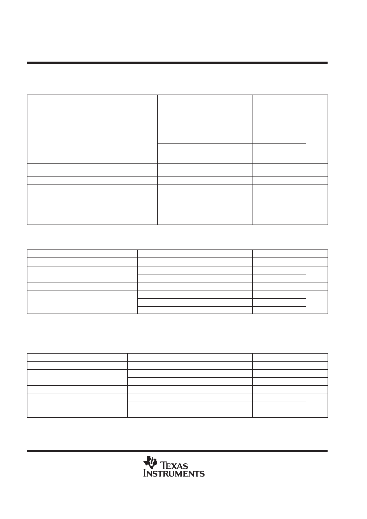
–10
–15
–20
–25
10 100 1 k 10 k
Relative Gain – dB
–5
0
f – Frequency – Hz
RELATIVE GAIN RESPONSE
vs
FREQUENCY
5
–30
–35
Figure 2. Receive Gain Response With Respect to Gain of 1 kHz Tone With High Pass Filter Selected and
High Pass Filter Disabled
receive idle channel noise and distortion, EAR1 selected, companded mode (µ-law or A-law) selected (see
Note 10)
PARAMETER TEST CONDITIONS MIN TYP MAX UNIT
Receive noise, psophometrically weighted PCMIN = 11010101 (A-law) –89 –86 dBm0
p
Receive noise, C-message weighted PCMIN = 11111111 (µ-law) 36 50 µV
rms
PCMIN to EAR1ON, EAR1OP at 3 dBm0 21
PCMIN to EAR1ON, EAR1OP at 0 dBm0 25
PCMIN to EAR1ON, EAR1OP at –5 dBm0 36
Receive signal-to-distortion ratio with 1020-Hz
PCMIN to EAR1ON, EAR1OP at –10 dBm0 43
Receive signal to distortion ratio with 1020 Hz
sinewave input
PCMIN to EAR1ON, EAR1OP at –20 dBm0 40
dB
PCMIN to EAR1ON, EAR1OP at –30 dBm0 38
PCMIN to EAR1ON, EAR1OP at –40 dBm0 28
PCMIN to EAR1ON, EAR1OP at –45 dBm0 23
NOTE 10: RXPGA = –4 dB for 32 Ω, RXVOL = 0 dB, 1020-Hz input signal at PCMI, output measured differentially between EAR1ON and EAR1OP.
Page 16

TWL1110
VOICE-BAND AUDIO PROCESSOR (VBAP)
SLWS103 – NOVEMBER 2000
16
POST OFFICE BOX 655303 • DALLAS, TEXAS 75265
electrical characteristics over recommended ranges of supply voltage and free-air temperature (unless
otherwise noted) (continued)
receive idle channel noise and distortion, EAR1 selected, linear mode selected (see Note 10)
PARAMETER TEST CONDITIONS MIN TYP MAX UNIT
Receive noise, (20-Hz to 20-kHz brickwall window) PCMIN = 000000000000000 –88 –83 dBm0
PCMIN to EAR1ON, EAR1OP at 3 dBm0 53 61
PCMIN to EAR1ON, EAR1OP at 0 dBm0 63 75
PCMIN to EAR1ON, EAR1OP at –5 dBm0 60 72
Receive signal-to-distortion ratio with 1020-Hz
PCMIN to EAR1ON, EAR1OP at –10 dBm0 56 67
Receive signal to distortion ratio with 1020 Hz
sine-wave input
PCMIN to EAR1ON, EAR1OP at –20 dBm0 50 63
dB
PCMIN to EAR1ON, EAR1OP at –30 dBm0 45 50
PCMIN to EAR1ON, EAR1OP at –40 dBm0 40 51
PCMIN to EAR1ON, EAR1OP at –45 dBm0 38 49
Intermodulation distortion, 2-tone CCITT method,
CCITT G.712 (7.1), R2 50
Intermodulation distortion, 2 tone CCITT method
,
composite power level, –13 dBm0
CCITT G.712 (7.2), R2 54
dB
NOTE 10: RXPGA = –4 dB for 32 Ω, RXVOL = 0 dB, 1020-Hz input signal at PCMI, output measured differentially between EAR1ON and EAR1OP.
receive idle channel noise and distortion EAR2 selected, companded mode (µ-law or A-law) selected
(see Note 11)
PARAMETER TEST CONDITIONS MIN TYP MAX UNIT
Receive noise, psophometrically weighted PCMIN = 11010101 (A-law) –82 –78 dBmo
p
Receive noise, C-message weighted PCMIN = 11111111 (µ-law) 36 50 µV
rms
PCMIN to EAR2O at 3 dBm0 21
PCMIN to EAR2O at 0 dBm0 25
PCMIN to EAR2O at –5 dBm0 36
Receive signal-to-distortion ratio with 1020-Hz sinewave
PCMIN to EAR2O at –10 dBm0 43
Receive signal-to-distortion ratio with 1020-Hz sinewave
input
PCMIN to EAR2O at –20 dBm0 40
dB
PCMIN to EAR2O at –30 dBm0 38
PCMIN to EAR2O at –40 dBm0 28
PCMIN to EAR2O at –45 dBm0 23
NOTE 11. RXPGA = –1 dB, RXVOL = 0 dB
receive idle channel noise and distortion, EAR2 selected, linear mode selected (see Note 11)
PARAMETER TEST CONDITIONS MIN TYP MAX UNIT
Receive noise, (20 Hz to 20 kHz brickwall window) PCMIN = 000000000000000 –83 –86 dBm0
PCMIN to EAR2O at 3 dBm0 53 60
PCMIN to EAR2O at 0 dBm0 60 65
PCMIN to EAR2O at –5 dBm0 58 62
Receive signal-to-noise + distortion ratio with 1020-Hz sinewave
p
PCMIN to EAR2O at –10 dBm0 55 60
input
PCMIN to EAR2O at –20 dBm0 53 60
dB
PCMIN to EAR2O at –30 dBm0 51 58
PCMIN to EAR2O at –40 dBm0 50 57
PCMIN to EAR2O at –45 dBm0 48 52
CCITT G.712 (7.1), R2 50
Intermodulation distortion, 2-tone CCITT method
CCITT G.712 (7.2), R2 54
dB
NOTE 11: RXPGA = –1 dB, RXVOL = 0 dB
Page 17

TWL1110
VOICE-BAND AUDIO PROCESSOR (VBAP)
SLWS103 – NOVEMBER 2000
17
POST OFFICE BOX 655303 • DALLAS, TEXAS 75265
electrical characteristics over recommended ranges of supply voltage and free-air temperature (unless
otherwise noted) (continued)
power supply rejection and crosstalk attenuation
PARAMETER TEST CONDITIONS MIN TYP MAX UNIT
Supply voltage rejection, transmit channel
MIC1N, MIC1P =0 V ,
VDD = 3 Vdc + 100 mV
peak to peak
, f = 0 to 50 kHz
– 86 –70 dB
Supply voltage rejection, receive channel,
EAR1 selected (differential)
PCM code = positive zero,
VDD = 3 Vdc + 100 mV
peak to peak
, f = 0 to 50 kHz
– 98 –70 dB
Crosstalk attenuation, transmit-to-receive
(differential)
MIC1N, MIC1P = 0 dB, f = 300 to 3400 Hz measured
differentially between EAR1ON and EAR1OP
70 dB
Crosstalk attenuation, receive-to-transmit
PCMIN = 0 dBm0, f = 300 to 3400 Hz measured at
PCMO, EAR1 amplifier
70 dB
switching characteristics
clock timing requirements for 2.048-MHz CLK
PARAMETER MIN NOM MAX UNIT
t
t
Transition time, MCLK 10 ns
f
(mclk)
MCLK frequency 2.048 MHz
MCLK jitter 37%
Number of PCMCLK clock cycles per PCMSYN frame 256 256
t
c(PCMCLK)
PCMCLK clock period 156 488 512 ns
Duty cycle, PCMCLK 45% 50% 68%
transmit timing requirements for 2.048-MHz CLK (see Figure 8)
PARAMETER MIN MAX UNIT
t
su(PCMSYN)
Setup time, PCMSYN high before falling edge of PCMCLK 20 t
c(PCMCLK)
–20
t
h(PCMSYN)
Hold time, PCMSYN high after falling edge of PCMCLK 20 t
c(PCMCLK)
–20
ns
receive timing requirements for 2.048-MHz CLK (see Figure 9)
PARAMETER MIN MAX UNIT
t
su(PCSYN)
Setup time, PCMSYN high before falling edge of PCMCLK 20 t
c(PCMCLK)
–20 ns
t
h(PCSYN)
Hold time, PCMSYN high after falling edge of PCMCLK 20 t
c(PCMCLK)
–20 ns
t
su(PCMI)
Setup time, PCMI high or low before falling edge of PCMCLK 20 ns
t
h(PCMI)
Hold time, PCMI high or low after falling edge of PCMCLK 20 ns
clock timing requirements for 128-kHz CLK
PARAMETER MIN NOM MAX UNIT
t
t
Transition time, MCLK 10 ns
f
(mclk)
MCLK frequency 128 kHz
MCLK jitter 5%
Number of PCMCLK clock cycles per PCMSYN frame 16 16
t
c(PCMCLK)
PCMCLK clock period 742.19 781.25 820.31 ns
Duty cycle, PCMCLK 40% 50% 60%
t
c(PCMSYN)
PCMSYN clock period 125 µs
Duty cycle, PCMCLK 49.5% 50% 50.5%
Page 18

TWL1110
VOICE-BAND AUDIO PROCESSOR (VBAP)
SLWS103 – NOVEMBER 2000
18
POST OFFICE BOX 655303 • DALLAS, TEXAS 75265
switching characteristics (continued)
transmit timing requirements for 128-kHz CLK (see Figure 12)
PARAMETER MIN MAX UNIT
t
su(PCMSYN)
Setup time, PCMSYN high before rising edge of PCMCLK 20 t
c(PCMCLK)
/4
t
h(PCMSYN)
Hold time, PCMSYN high after falling edge of PCMCLK 20 t
c(PCMCLK)
/4
ns
t
v(PCMO)
Data valid time after the rising edge of PCMSYNC 50 ns
receive timing requirements for 128-kHz CLK (see Figure 11)
PARAMETER MIN MAX UNIT
t
su(PCSYN)
Setup time, PCMSYN high before rising edge of PCMCLK 20 t
c(PCMCLK)
/4 ns
t
h(PCSYN)
Hold time, PCMSYN high after falling edge of PCMCLK 20 t
c(PCMCLK)
/4 ns
t
su(PCMI)
Setup time, PCMI high or low before falling edge of PCMCLK 20 ns
t
h(PCMI)
Hold time, PCMI high or low after falling edge of PCMCLK 20 ns
propagation delay times, C
Lmax
= 10 pF (see Figure 8)
PARAMETER MIN MAX UNIT
t
pd1
From PCMCLK bit 1 high to PCMO bit 1 valid 35 ns
t
pd2
From PCMCLK high to PCMO valid, bits 2 to n 35 ns
t
pd3
From PCMCLK bit n low to PCMO bit n Hi-Z 30 ns
I2C bus timing requirements (see Figure 10)
PARAMETER MIN MAX UNIT
SCL Clock frequency 400 kHz
t
(HIGH)
Clock high time 600 ns
t
(LOW)
Clock low time 1300 ns
t
h(STA)
Hold time (repeated) ST ART condition. After this period the first clock pulse is generated. 600 ns
t
su(STA)
Setup time for repeated STAR T condition 600 ns
t
h(DAT)
Data input hold time 0 ns
t
su(DAT)
Data input setup time 100 ns
t
su(STO)
STOP condition setup time 600 ns
t
(BUF)
Bus free time 1300 ns
t
r
SDA and SCL rise time 300 ns
t
f
SDA and SCL fall time 300 ns
DTMF generator characteristics
PARAMETER TEST CONDITIONS MIN TYP MAX UNIT
DTMF high to low tone relative amplitude (pre-emphasis) 1.5 2 2.5 dB
Tone frequency accuracy (for DTMF) Resolution of 7.8125 Hz –1.5 1.5 %
Harmonic distortion
Measured from lower tone group to
highest parasitic
–20 dB
MICBIAS characteristics
PARAMETER TEST CONDITIONS MIN TYP MAX UNIT
Load impedance (bias mode) 5 kΩ
Page 19

TWL1110
VOICE-BAND AUDIO PROCESSOR (VBAP)
SLWS103 – NOVEMBER 2000
19
POST OFFICE BOX 655303 • DALLAS, TEXAS 75265
PARAMETER MEASUREMENT INFORMATION
NOTE: SLAVE = VBAP
A6 A5 A4 A0 R/W0ACK
0
R7 R6 R5 R0 ACK
0
D7 D6 D5 D0 ACK
0
Stop
Slave Address Register Address Data
SCL
SDA
Start
Figure 3. I2C-Bus Write to VBAP
NOTE: SLAVE = VBAP
Master
Drives
ACK and Stop
A6 A5 A0 R/W ACK
00
R7 R6 R0 ACK A6 A0 R/W ACK
10
D7 D6 D0 ACK
Slave Address Register Address Slave Address
Slave Drives
The Data
Repeated
Start
SCL
SDA
Start Stop
Figure 4. I2C Read From VBAP: Protocol A
NOTE: SLAVE = VBAP
A6 A5 A0 R/W ACK R7
00
R6 R0 ACK A6 A5 A0
R/W ACK
D7 D0
ACK
Master
Drives
ACK and Stop
Slave Address Register Address Slave Address
Slave Drives
The Data
Stop
Stop Start
SCL
SDA
Start
Figure 5. I2C Read From VBAP: Protocol B
Page 20

TWL1110
VOICE-BAND AUDIO PROCESSOR (VBAP)
SLWS103 – NOVEMBER 2000
20
POST OFFICE BOX 655303 • DALLAS, TEXAS 75265
PRINCIPLES OF OPERATION
power-on initialization
An external reset with a minimum pulse width of 500 ns must be applied to the active low RESET terminal to
guarantee reset upon power on. All registers are set with default values upon external reset initialization.
The desired selection for all programmable functions can be initialized prior to a power-up command using the
control interface.
Table 1. Power Up and Power Down Procedures (V
DD
= 2.7 V, earphone amplifier unloaded)
DEVICE STATUS PROCEDURE
MAXIMUM POWER
CONSUMPTION
Set bit 1 = 1 in power control register, EAR1 enabled 16.2 mW
Power up
Set bit 1 = 0 in power control register, EAR2 enabled 14.6 mW
Set bit 7 = 1 in TXPGA control register and bit 0 = 0 1.35 µW
Power down
Set bit 7 = 0 in TXPGA control register and bit 0 = 0 67.5 µW
In addition to resetting the power down bit in the power control register, loss of MCLK (no transition detected)
automatically enters the device into a power down state with PCMO in the high impedance state. If during a pulse
code modulation (PCM) data transmit cycle an asynchronous power down occurs, the PCM interface remains
powered up until the PCM data is completely transferred.
An additional power down mode overrides the MCLK detection function. This allows the device to enter the
power down state without regard to MCLK. Setting bit 7 of the TXPGA sidetone register to logic high enables
this function.
internal reference current setting terminal
Use a 100-kΩ precision resistor to connect the REXT pin to GND.
conversion laws
The device can be programmed for either a 15-bit linear or and 8-bit (µ-law or A-law) companding mode. The
companding operation approximates the CCITT G.711 recommendation. The linear mode operation uses a
15-bit twos-complement format.
transmit operation
microphone input
The microphone input stage is a low-noise differential amplifier that provides a preamplifier gain of 23.5 dB. It
is recommended that a microphone capacitively connected to the MIC1N and MIC1P inputs, while the MIC2N
and MIC2P inputs can be used to capacitively connect a second microphone or an auxiliary audio circuit.
Page 21

TWL1110
VOICE-BAND AUDIO PROCESSOR (VBAP)
SLWS103 – NOVEMBER 2000
21
POST OFFICE BOX 655303 • DALLAS, TEXAS 75265
PRINCIPLES OF OPERATION
transmit operation (continued)
_
+
_
+
V
ref
510 kΩ
510 kΩ
34 kΩ
34 kΩ
Ci MIC1N
Ci MIC1P
M
I
C
R
mic
R
mic
MBIAS
Figure 6. Typical Microphone Interface
microphone mute function
Transmit channel muting provides 80-dB attenuation of the input microphone signal. The MICMUTE function
can be selected by setting bit 6 of the power control register through the I2C interface.
transmit channel gain control
The values in the transmit PGA control registers control the gain in the transmit path. The total TX channel gain
can vary from 41.5 dB to 19.5 dB. The default total TX channel gain is 23.5 dB.
Table 2. Transmit Gain Control
BIT NAME MIC AMP1 MIC AMP2 TX PGA
GAIN
MODE
TOTAL TX GAIN
TP3 TP2 TP1 TP0 GAIN GAIN GAIN MIN TYP MAX UNIT
0 0 0 0 23.5 18 0 Extended 41.3 41.5 41.7 dB
0 0 0 1 23.5 18 –2 Extended 39.3 39.5 39.7 dB
0 0 1 0 23.5 18 –4 Extended 37.3 37.5 37.7 dB
0 0 1 1 23.5 18 –6 Extended 35.3 35.5 35.7 dB
0 1 0 0 23.5 18 –8 Extended 33.3 33.5 33.7 dB
0 1 0 1 23.5 18 –10 Extended 31.3 31.5 31.7 dB
1 0 0 0 23.5 6 0 Normal 29.3 29.5 29.7 dB
1 0 0 1 23.5 6 –2 Normal 27.3 27.5 27.7 dB
1 0 1 0 23.5 6 –4 Normal 25.3 25.5 25.7 dB
1 0 1 1 23.5 6 –6 Normal 23.3 23.5 23.7 dB
1 1 0 0 23.5 6 –8 Normal 21.3 21.5 21.7 dB
1 1 0 1 23.5 6 –10 Normal 19.3 19.5 19.7 dB
Page 22

TWL1110
VOICE-BAND AUDIO PROCESSOR (VBAP)
SLWS103 – NOVEMBER 2000
22
POST OFFICE BOX 655303 • DALLAS, TEXAS 75265
PRINCIPLES OF OPERATION
receive operation
receive channel gain control
The values in the receive PGA control registers control the gain in the receive path. PGA gain is set from
–6 to 6 dB in 1-dB steps through the I2C interface. The default receive channel gain is –4 dB.
Table 3. Receive PGA Gain Control
BIT NAME RELATIVE GAIN, VOICE MODE
RP3 RP2 RP1 RP0 MIN TYP MAX UNIT
DTMF GAIN, TONE NODE
0 0 0 0 5.8 6 6.2 dB 12
0 0 0 1 4.8 5 5.2 dB 12
0 0 1 0 3.8 4 4.2 dB 12
0 0 1 1 2.8 3 3.2 dB 6
0 1 0 0 1.8 2 2.2 dB 6
0 1 0 1 0.8 1 1.2 dB 6
0 1 1 0 –0.2 0 0.2 dB 0
0 1 1 1 –1.2 –1 –0.8 dB 0
1 0 0 0 –2.2 –2 –1.8 dB 0
1 0 0 1 –3.2 –3 –2.8 dB –6
1 0 1 0 –4.2 –4 –3.8 dB –6
1 0 1 1 –5.2 –5 –4.8 dB –6
1 1 0 0 –6.2 –6 –5.8 dB –12
1 1 0 1 X dB –12
1 1 1 0 X dB –12
sidetone gain control
The values in the sidetone PGA control registers control the sidetone gain. Sidetone gain is set from –12 dB
to –24 dB in 2-dB steps through the I2C interface. Sidetone can be muted by setting bit 7 of the power control
register. The default sidetone gain is –12 dB.
Table 4. Sidetone Gain Control
BIT NAME RELATIVE GAIN
ST2 ST1 ST0 MIN TYP MAX UNIT
0 0 0 –12.2 –12 –11.8 dB
0 0 1 –14.2 –14 –13.8 dB
0 1 0 –16.2 –16 –15.8 dB
0 1 1 –18.2 –18 –17.8 dB
1 0 0 –20.2 –20 –19.8 dB
1 0 1 –22.2 –22 –21.8 dB
1 1 0 –24.2 –24 –23.8 dB
Page 23

TWL1110
VOICE-BAND AUDIO PROCESSOR (VBAP)
SLWS103 – NOVEMBER 2000
23
POST OFFICE BOX 655303 • DALLAS, TEXAS 75265
PRINCIPLES OF OPERATION
receive operation (continued)
receive volume control
The values in the volume control PGA control registers provide volume control for the earphone. Volume control
gain is set from 0 dB to –18 dB in 2-dB steps through the I2C interface. The default RX volume control gain is
0 dB.
Table 5. RX Volume Control
BIT NAME RELATIVE GAIN
RV3 RV2 RV1 RV0 MIN TYP MAX UNIT
0 0 0 0 –0.2 0 0.2 dB
0 0 0 1 –2.2 –2 –1.8 dB
0 0 1 0 –4.2 –4 –3.8 dB
0 0 1 1 –6.2 –6 –5.8 dB
0 1 0 0 –8.2 –8 –7.8 dB
0 1 0 1 –10.2 –10 –9.8 dB
0 1 1 0 –12.2 –12 –11.8 dB
0 1 1 1 –14.2 –14 –13.8 dB
1 0 0 0 –16.2 –16 –15.8 dB
1 0 0 1 –18.2 –18 –17.8 dB
earphone amplifier
The analog signal can be routed to either of two earphone amplifiers: one with a differential output (EAR1ON
and EAR1OP) capable of driving a 8-Ω load, or one with a single-ended output (EAR2O) capable of driving a
8-Ω load.
earphone mute function
Muting can be selected by setting bit 3 of the power control register through the I
2
C interface.
receive PCM data format
Companded mode: 8 bits are received, the most significant (MSB) first.
Linear mode: 15 bits are received, MSB first.
Page 24

TWL1110
VOICE-BAND AUDIO PROCESSOR (VBAP)
SLWS103 – NOVEMBER 2000
24
POST OFFICE BOX 655303 • DALLAS, TEXAS 75265
PRINCIPLES OF OPERATION
receive operation (continued)
Table 6. Receive-Data Bit Definitions
BIT NO. COMPANDED
MODE
LINEAR
MODE
1 CD7 LD14
2 CD6 LD13
3 CD5 LD12
4 CD4 LD11
5 CD3 LD10
6 CD2 LD9
7 CD1 LD8
8 CD0 LD7
9 – LD6
10 – LD5
11 – LD4
12 – LD3
13 – LD2
14 – LD1
15 – LD0
16 – ––
Transmit channel gain control bits always follow the PCM data in time:
CD7-CD0 = data word in companded mode
LD14-LD0 = data word in linear mode
DTMF generator operation and interface
The DTMF circuit generates the summed DTMF tones for push button dialing and provides the PDM output for
the BUZZCON user-alert tone. The integer value is determined by the formula round tone [Freq (Hz)/resolution
(Hz)]. The integer value is loaded into one of two 8-bit registers, high tone register (04) or low tone register (05).
The tone output is 2 dB higher when applied to the high tone register (04). When generating DTMF tones, the
high frequency value must be applied to the high tone register (04) and the low DTMF value to the low tone
register.
The DTMF frequency resolution is controlled by the auxiliary register (06) bits 2, 3, 4, and 5. When the resolution
is set to 7.8125 Hz, the frequency range can be up to 1992.2 Hz. A wider range can be accomplished (for
example, 2x or 4x) by selecting lower resolutions of 15.625 Hz or 31.250 Hz. The gain setting is controlled by
the RXPGA gain control. This register applies the required gain to obtain MUX control during tone mode
operation. Table 3 shows the relationship of the two gain settings.
Page 25

TWL1110
VOICE-BAND AUDIO PROCESSOR (VBAP)
SLWS103 – NOVEMBER 2000
25
POST OFFICE BOX 655303 • DALLAS, TEXAS 75265
PRINCIPLES OF OPERATION
DTMF generator operation and interface (continued)
Table 7. Typical DTMF and Single Tone Control
DT7 DT6 DT5 DT4 DT3 DT2 DT1 DT0
INTEGER
VALUE
TONE
FUNCTION
TONE/HZ
0 1 0 1 1 0 0 1 89 DTMF Low 697
0 1 1 0 0 0 1 1 99 DTMF Low 770
0 1 1 0 1 1 0 1 109 DTMF Low 852
0 1 1 1 1 0 0 0 120 DTMF Low 941
1 0 0 1 1 0 1 1 155 DTMF HIgh 1209
1 0 1 0 1 0 1 1 171 DTMF HIgh 1336
1 0 1 1 1 1 0 1 189 DTMF HIgh 1477
1 1 0 1 0 0 0 1 209 DTMF HIgh 1633
T ones from the DTMF generator block are present at all outputs and are controlled by enabling or disabling the
individual output ports. The values that determine the tone frequency are loaded into the tone registers (high
and low) as two separate values.
The values loaded into the tone registers initiate an iterative table look-up function, placing a 6-bit or 7-bit in
twos-complement value into the the tone registers. There is a 2-dB difference in the resulting output of the two
registers, the high-tone register having the greater result.
In the case of low-tone signal, the tone generator outputs a 6-bit integer with a maximum code of 31 (01 1111).
However, the DTMF output is an 8-bit integer . Therefore, two zeros are padded to the MSB position which results
in 31 (00011111). On the other hand, the receive channel requires a 15-bit integer, the input 3968
(000111110000000). Since the maximum digital value of receive channel is 16383 (011111111111111), the
maximum low-tone signal is designed to be –12.32 dB below the full digital scale.
20 log
3968
16383
2
–12.32 dB
In the case of high-tone signal, the tone generator outputs a 7-bit integer with a maximum code of 39 (01001 11).
The DTMF, therefore, pads a zero to the MSB and generates an 8-bit integer (001001 11). In order to send the
digital code to receive channel, it is converted to a 15-bit integer with seven more zeros padded to LSB position
and biased as 4992 (001001 110000000). Therefore, the maximum high-tone signal is designed to be –10.32 dB
below the full digital scale.
20 log
4992
16383
2
–10.32 dB
In the case of DTMF output, the tone generator outputs an 8-bit integer with the maximum code level of 70
(01000110). This output is converted to a 15-bit code with the value of 8960 (010001100000000). Therefore,
the maximum output of DTMF is designed to be –5.24 dB below the full digital scale.
20 log
8960
16383
2
–5.24 dB
(1)
(2)
(3)
Page 26

TWL1110
VOICE-BAND AUDIO PROCESSOR (VBAP)
SLWS103 – NOVEMBER 2000
26
POST OFFICE BOX 655303 • DALLAS, TEXAS 75265
PRINCIPLES OF OPERATION
buzzer logic section
The single-ended output BUZZCON is a PDM signal intended to drive a buzzer through an external driver
transistor. The PDM begins as a selected DTMF tone, generated and passed through the receive D/A channel
and fed back to the transmit channel analog modulator, where a PDM signal is generated and routed to the
BUZZCON output.
Buzzcon
DTMF
DTMF
Gain
Mux
Digital
Modulator
and
Filter
Analog
Modulator
Buzzer
Control
Figure 7. Buzzer Driver System Architecture
support section
The clock generator and control circuit use the master clock input (MCLK) to generate internal clocks to drive
internal counters, filters, and convertors. Register control data is written into and read back from the VBAP
registers via the control interface.
I
2
C-bus protocols
The VBAP serial interface is designed to be I2C bus-compatible and operates in the slave mode when CE is
high. This interface consists of the following terminals:
SCL: I2C-bus serial clock—This input synchronizes the control data transfer to and from the codec.
SDA: I2C-bus serial address/data input/output—This is a bidirectional terminal that transfers register
control addresses and data into and out of the codec. It is an open drain terminal and therefore
requires a pullup resistor to VCC (typical 10 kΩ for 100 kHz).
TWL1110 has a fixed device select address of (E2)HEX for write mode and (E3)HEX for read mode.
For normal data transfer, SDA is allowed to change only when SCL is low. Changes when SCL is high are
reserved for indicating the start and stop conditions.
Data transfer may be initiated only when the bus is not busy. During data transfer, the data line must remain
stable whenever the clock line is at high. Changes in the data line while the clock line is at high are interpreted
as a start or stop condition.
Table 8. I2C-Bus Conditions
CONDITION STATUS DESCRIPTION
A Bus not busy Both data and clock lines remain at high.
B Start data transfer
A high to low transition of the SDA line while the clock (SCL) is high determines a start condition.
All commands must proceed from a start condition.
C Stop data transfer
A low to high transition of the SDA line while the clock (SCL) is high determines a stop condition.
All operations must end with a stop condition.
D Data valid
The state of the data line represents valid data when, after a start condition, the data line is stable
for the duration of the high period of the clock signal.
The data on the line must be changed during the low period of the clock signal. There is one clock pulse per
bit of data.
Page 27

TWL1110
VOICE-BAND AUDIO PROCESSOR (VBAP)
SLWS103 – NOVEMBER 2000
27
POST OFFICE BOX 655303 • DALLAS, TEXAS 75265
PRINCIPLES OF OPERATION
I2C-bus protocols (continued)
Each data transfer is initiated with a start condition and terminated with a stop condition. The number of data
bytes, transferred between the start and stop conditions, is determined by the master device (microprocessor).
When addressed, the VBAP generates an acknowledge after the reception of each byte. The master device
must generate an extra clock pulse that is associated with this acknowledge bit.
The VBAP must pull down the SDA line during the acknowledge clock pulse so that the SDA line is at stable
low state during the high period of the acknowledge related clock pulse. Setup and hold times must be taken
into account. During read operations, the master device must signal an end of data to the slave by not generating
an acknowledge bit on the last byte that was clocked out of the slave. In this case, the slave (VBAP) must leave
the data line high to enable the master device to generate the stop condition.
clock frequencies and sample rates
A fixed PCMSYN rate of 8 kHz determines the sampling rate.
register map addressing
BITS
REG
07 06 05 04 03 02 01 00
Power control 00 Sidetone En TXEn RX TX En MICSEL BIASEn RXEn
EAROUT
Sel
PWRUP
Mode control 01 Comp Sel TMEn PCMLB Comp En BUZZEn
RXFLTREnTXFLTREnTXSLOPE
En
TXPGA 02 X TP3 TP2 TP1 TP0 ST2 ST1 ST0
RXPGA 03 RP3 RP2 RP1 RP0 RV3 RV2 RV1 RV0
High DTMF 04
HIFREQ
Sel7
HIFREQ
Sel6
HIFREQ
Sel5
HIFREQ
Sel4
HIFREQ
Sel3
HIFREQ
Sel2
HIFREQ
Sel1
HIFREQ
Sel0
Low DTMF 05
LOFREQ
Sel7
LOFREQ
Sel6
LOFREQ
Sel5
LOFREQ
Sel4
LOFREQ
Sel3
LOFREQ
Sel2
LOFREQ
Sel1
LOFREQ
Sel0
AUX 06
MCLK
Detect
RXPGA2
†
DTMFH1 DTMFH0 DTML1 DTMFL0 AMVX MCLK sel
†
For voice mode only
Page 28

TWL1110
VOICE-BAND AUDIO PROCESSOR (VBAP)
SLWS103 – NOVEMBER 2000
28
POST OFFICE BOX 655303 • DALLAS, TEXAS 75265
PRINCIPLES OF OPERATION
register power-up defaults
BITS
REG
07 06 05 04 03 02 01 00
Power control (1)
†
00 1 1 1 1 0 1 1 0
Power control (2)
‡
00 1 0 0 1 1 0 1 1
Mode control 01 0 0 0 0 0 0 1 0
TXPGA 02 0 1 0 0 0 0 0 0
RXPGA 03 1 0 1 0 0 0 0 0
High DTMF 04 0 0 0 0 0 0 0 0
Low DTMF 05 0 0 0 0 0 0 0 0
AUX 06 0 0 0 0 0 0 0 0
†
1. Value when PWRUPSEL = 0
‡
2. Value when PWRUPSEL = 1
register map
Table 9. Power Control Register: Address (00) HEX
BIT NUMBER
7 6 5 43210
DEFINITIONS
1 1 1 1 0 1 1 0 Default setting PWRUPSEL = 0
1 0 0 11011Default setting PWRUPSEL = 1
X X X X X X X 0 Reference system, power down
X X X X X X X 1 Reference system, power up
X X X X X X 1 X EAR AMP1 selected, EAR AMP2 power down
X X X X X X 0 X EAR AMP2 selected, EAR AMP1 power down
X X X X X 0 X X Receive channel enabled
X X 0 X X 1 X X Receive channel muted
X X 1 X X 1 X 0 Receive channel, power down
X X X X 1 X X X Micbias enable
X X X X 0 X X X Micbias disable
X X X 1XXXXMIC1 selected
X X X 0XXXXMIC2 selected
X 0 X XXXXXTransmit channel enabled
X 1 0 XXXXXTransmit channel muted
X 1 1 XXXXXTransmit channel power down
0 XXXXXXXSidetone enabled
1 X X X X X X X Sidetone muted
Page 29

TWL1110
VOICE-BAND AUDIO PROCESSOR (VBAP)
SLWS103 – NOVEMBER 2000
29
POST OFFICE BOX 655303 • DALLAS, TEXAS 75265
PRINCIPLES OF OPERATION
register map (continued)
Table 10. Mode Control Register: Address (01) HEX
BIT NUMBER
7 6543210
DEFINITIONS
0 0 0 0 0 0 1 0 Default setting
X X X X X X 0 0 TX channel high-pass filter enabled and slope filter enabled
X X X X X X 0 1 TX channel high-pass filter enabled and slope filter disabled
X X X X X X 1 0 TX channel high-pass filter disabled and slope filter enabled
X X X X X X 1 1 TX channel high-pass filter disabled and slope filter disabled
X X X X X 0 X X RX channel high-pass filter disabled (low pass only)
X X X X X 1 X X RX channel high-pass filter enabled
X X X X 0 X X X BUZZCON disabled
X X X X 1 X X X BUZZCON enabled
X X X 0 X X X X Linear mode selected
1 X X 1 X X X X A-law companding mode selected
0 XX1XXXXµ-law companding mode selected
X X 0 X X X X X TX and RX channels normal mode
X X 1 X X X X X PCM loopback mode
X 0 X X X X X X Tone mode disabled
X 1 X X X X X X Tone mode enabled
Page 30

TWL1110
VOICE-BAND AUDIO PROCESSOR (VBAP)
SLWS103 – NOVEMBER 2000
30
POST OFFICE BOX 655303 • DALLAS, TEXAS 75265
PRINCIPLES OF OPERATION
register map (continued)
Transmit PGA and sidetone control register: Address (02)HEX
Bit definitions:
7 6 5 4 3 2 1 0 DEFINITION
X TP3 TP2 TP1 TP0 ST2 ST1 ST0 See Table 2 and Table 4
0 1 0 0 0 0 0 0 Default setting
Receive volume control register: Address (03)HEX
Bit definitions:
7 6 5 4 3 2 1 0 DEFINITION
RP3 RP2 RP1 RP0 RV3 RV2 RV1 RV0 See Table 3 and Table 5
1 0 1 0 0 0 0 0 Default setting
High tone selection control register: Address (04)HEX
Bit definitions:
7 6 5 4 3 2 1 0 DEFINITION
X X X X X X X X DTMF (see Table 7)
0 0 0 0 0 0 0 0 Default setting
Low tone selection control register: Address (05)HEX
Bit definitions :
7 6 5 4 3 2 1 0 DEFINITION
X X X X X X X X DTMF (see Table 7)
0 0 0 0 0 0 0 0 Default setting
Auxiliary register: Address (06)HEX
Bit definitions:
7 6 5 4 3 2 1 0 DEFINITION
0 0 0 0 0 0 0 0 Default
X X X X X X X 0 MCLK is set to 2.048 MHz
X X X X X X X 1 MCLK is set to 128 MHz
X X X X X X 0 X Analog switch output is set to OUT2
X X X X X X 1 X Analog switch output is set to OUT1
X X X X 0 0 X X Low tone frequency resolution is set to 7.8125 Hz
X X X X 0 1 X X Low tone frequency resolution is set to 15.625 Hz
X X X X 1 0 X X Low tone frequency resolution is set to 31.250 Hz
X X 0 0 X X X X High tone frequency resolution is set to 7.8125 Hz
X X 0 1 X X X X High tone frequency resolution is set to 15.625 Hz
X X 1 0 X X X X High tone frequency resolution is set to 31.250 Hz
X 0 X X X X X X Receiver channel gain, RXPGA2 is equal to 0 dB, voice mode only
X 1 X X X X X X Receiver channel gain, RXPGA2 is equal to 6 dB, voice mode only
0 X X X X X X X MCLK detector is powered ON
1 X X X X X X X MCLK detector is powered OFF
Page 31

TWL1110
VOICE-BAND AUDIO PROCESSOR (VBAP)
SLWS103 – NOVEMBER 2000
31
POST OFFICE BOX 655303 • DALLAS, TEXAS 75265
PRINCIPLES OF OPERATION
using VBAP as a general purpose voice codec
In situations when a general purpose voice codec is needed and programming features are not necessary , the
receive and transmit channels can be enabled for voice mode only by setting the powerup select pin to VCC level.
When set to default, the following features are activated:
REF is powered up
Ear Amp1 selected, Ear Amp 2 = OFF
Receive channel enabled
MIC bias enabled
MIC 2 selected
Transmit channel enabled
Side tone enabled – Gain = –12 dB
TX channel high pass filter disabled
TX channel slope filter enabled
RX channel HP filter disabled (low pass only)
Buzzcon disabled
Linear mode only
TX and RX channel normal mode (no loopback)
Tone mode disabled (voice mode only)
MIC Amp 1 gain = 23.5 dB
MIC Amp 2 gain = 6 dB
TX PGA gain = 0 dB
Total TX gain = 29.5 dB
Receive PGA = –4 dB
Receive PGA 2 = 0 dB
Volume = 0 dB
Total RX gain = –4 dB
Clock = 2.048 MHz
Page 32

TWL1110
VOICE-BAND AUDIO PROCESSOR (VBAP)
SLWS103 – NOVEMBER 2000
32
POST OFFICE BOX 655303 • DALLAS, TEXAS 75265
PRINCIPLES OF OPERATION
0 1 2 3 4 N–2 N–1 N N+1
Transmit T ime Slot
1 2 3 4 N–2 N–1 N
80%
20%
t
su(PCMSYN)
t
h(PCMSYN)
See Note A
See Note C
See Note B
t
pd2
t
pd1
See Note D
t
su(PCMO)
t
pd3
80%
20%
PCMCLK
PCMSYN
PCMO
NOTES: A. This window is allowed for PCMSYN high.
B. This window is allowed for PCMSYN low (t
h(PCMSYN)
max determined by data collision considerations).
C. Transitions are measured at 50%.
D. Bit 1 = MSB, Bit N = LSB
Figure 8. Transmit Timing Diagram (2.048 MHz)
80%
20%
See Note C
PCMI
PCMSYN
PCMCLK
0 1 2 3 4 N –2 N –1 N N +1
20%
80%
1 2 3 4 N –2 N –1 N
See Note D
t
h(PCMSYN)
t
su(PCMSYN)
See Note A
t
su(PCMI)
t
h(PCMI)
See Note B
Receive Time Slot
NOTES: A. This window is allowed for PCMSYN high.
B. This window is allowed for PCMSYN low.
C. Transitions are measured at 50%.
D. Bit 1 = MSB, Bit N = LSB
Figure 9. Receive Timing Diagram (2.048 MHz)
t
(BUF)
t
hd(STA)
t
(Low)
t
r
t
f
t
hd(DAT)
t
(HIGH)
t
su(DAT)
t
su(STA)
t
hd(STA)
t
su(STO)
STO STA STA STO
SDA
SCL
Figure 10. I2C-Bus Timing Diagram
Page 33

TWL1110
VOICE-BAND AUDIO PROCESSOR (VBAP)
SLWS103 – NOVEMBER 2000
33
POST OFFICE BOX 655303 • DALLAS, TEXAS 75265
PRINCIPLES OF OPERATION
PCMSYNC
PCMI
PCMCLK
t
su(PCMSYN)
t
su(PCMI)
t
h(PCMSYN)
t
h(PCMI)
MSB
LSB
Figure 11. Receive T iming Diagram, 128 kHz
PCMSYNC
PCMO
PCMCLK
t
su(PCMSYN)
t
v(PCMO)
t
h(PCMSYN)
MSB LSB
Figure 12. Transmit Timing Diagram, 128 kHz
t
c(PCMSYNC)
Figure 13. PCMSYNC Timing, 128 kHz
Page 34

TWL1110
VOICE-BAND AUDIO PROCESSOR (VBAP)
SLWS103 – NOVEMBER 2000
34
POST OFFICE BOX 655303 • DALLAS, TEXAS 75265
PRINCIPLES OF OPERATION
VBAP device comparisons
TWL1102, 03 TWL1110 TWL1112
Single tone frequency range To 2 kHz To 8 kHz To 8 kHz
Transmit channel gain range 13.5 dB to 35.5 dB 19.5 dB to 41.5 dB 19.5 dB to 41.5 dB
Receive channel gain range – 24 dB to 6 dB – 24 dB to 12 dB – 24 dB to 12 dB
PCMCLK rate 2.048 MHz 128 kHz or 2.048 MHz 128 kHz or 2.048 MHz
Device pin out Backward compatible (TQFP)
Control registers Backward compatible
Number of registers 6 7 7
Control interface I2C I2C DISB
Analog switch No Yes No
Earout driving impedance 32 Ω 8-32 Ω 8-32 Ω
DTMF Yes Yes Yes
Tone resolution (Hz) 7.8125
7.8125
15.625
31.250
7.8125
15.625
31.250
Packages TQFP
TQFP,
MicroStar Junior BGA
TQFP,
MicroStar Junior BGA
MicroStar Junior BGA is a trademark of Texas Instruments.
Page 35

TWL1110
VOICE-BAND AUDIO PROCESSOR (VBAP)
SLWS103 – NOVEMBER 2000
35
POST OFFICE BOX 655303 • DALLAS, TEXAS 75265
MECHANICAL DATA
PBS (S-PQFP-G32) PLASTIC QUAD FLATPACK
Gage Plane
16
9
0,13 NOM
0,25
0,40
0,70
Seating Plane
0,10 MIN
4087735/A 11/95
17
0,17
0,23
8
5,05
4,95
SQ
3,50 TYP
24
25
1
32
6,90
7,10
SQ
1,05
0,95
1,20 MAX
0,08
0,50
M
0,08
0°–7°
NOTES: A. All linear dimensions are in millimeters.
B. This drawing is subject to change without notice.
Page 36

TWL1110
VOICE-BAND AUDIO PROCESSOR (VBAP)
SLWS103 – NOVEMBER 2000
36
POST OFFICE BOX 655303 • DALLAS, TEXAS 75265
MECHANICAL DATA
GQE (S-PBGA-N80) PLASTIC BALL GRID ARRAY
98765
J
H
G
F
E
D
321
C
B
A
4
4,00 TYP
Seating Plane
5,20
4,80
SQ
0,62
0,68
0,25
0,35
1,00 MAX
0,50
0,50
0,08
M
∅ 0,05
4200461/B 04/00
0,11
0,21
NOTES: A. All linear dimensions are in millimeters.
B. This drawing is subject to change without notice.
C. MicroStar Junior BGA configuration
MicroStar Junior BGA is a trademark of Texas Instruments.
Page 37

IMPORTANT NOTICE
T exas Instruments and its subsidiaries (TI) reserve the right to make changes to their products or to discontinue
any product or service without notice, and advise customers to obtain the latest version of relevant information
to verify, before placing orders, that information being relied on is current and complete. All products are sold
subject to the terms and conditions of sale supplied at the time of order acknowledgment, including those
pertaining to warranty, patent infringement, and limitation of liability.
TI warrants performance of its semiconductor products to the specifications applicable at the time of sale in
accordance with TI’s standard warranty. T esting and other quality control techniques are utilized to the extent
TI deems necessary to support this warranty. Specific testing of all parameters of each device is not necessarily
performed, except those mandated by government requirements.
Customers are responsible for their applications using TI components.
In order to minimize risks associated with the customer’s applications, adequate design and operating
safeguards must be provided by the customer to minimize inherent or procedural hazards.
TI assumes no liability for applications assistance or customer product design. TI does not warrant or represent
that any license, either express or implied, is granted under any patent right, copyright, mask work right, or other
intellectual property right of TI covering or relating to any combination, machine, or process in which such
semiconductor products or services might be or are used. TI’s publication of information regarding any third
party’s products or services does not constitute TI’s approval, warranty or endorsement thereof.
Copyright 2000, Texas Instruments Incorporated
 Loading...