

Page 1
D
Universal Serial Bus (USB) Version 1.1
Compliant
D
Integrated USB Transceivers
D
3.3-V Low Power ASIC Logic
D
One Upstream Port and 2-3 Programmable
Downstream Ports
– Total Number of Ports (2 or 3) Selected
by Input Pin
– Total Number of Permanently Connected
Ports Is Selected by 2 Input Pins
D
Two Power Source Modes
– Self-Powered Mode
– Bus-Powered Mode
D
All Downstream Ports Support Full-Speed
and Low-Speed Operations
D
Power Switching and Overcurrent
Reporting Is Provided Per Port or Ganged
D
Supports Suspend and Resume Operations
D
Suspend Status Terminal Available for
External Logic Power Down
TUSB2036
2/3-PORT HUB FOR THE UNIVERSAL SERIAL BUS
WITH OPTIONAL SERIAL EEPROM INTERFACE
SLLS372 – MARCH 2000
D
Supports Custom Vendor ID and Product ID
With External Serial EEPROM
D
3-State EEPROM Interface Allows EEPROM
Sharing
D
Push-Pull Outputs for PWRON Eliminate
the Need for External Pullup Resistors
D
Noise Filtering on OVRCUR Provides
Immunity to Voltage Spikes
D
Supports 6 MHz Operation Through Crystal
Input or 48 MHz Input Clock
D
Output Pin Available to Disable External
Pullup Resister on DP0 for 3 ms After Reset
or After Change on BUSPWR and Enable
Easy Implementation of On-Board Bus/Self
Power Dynamic Switching Circuitry
D
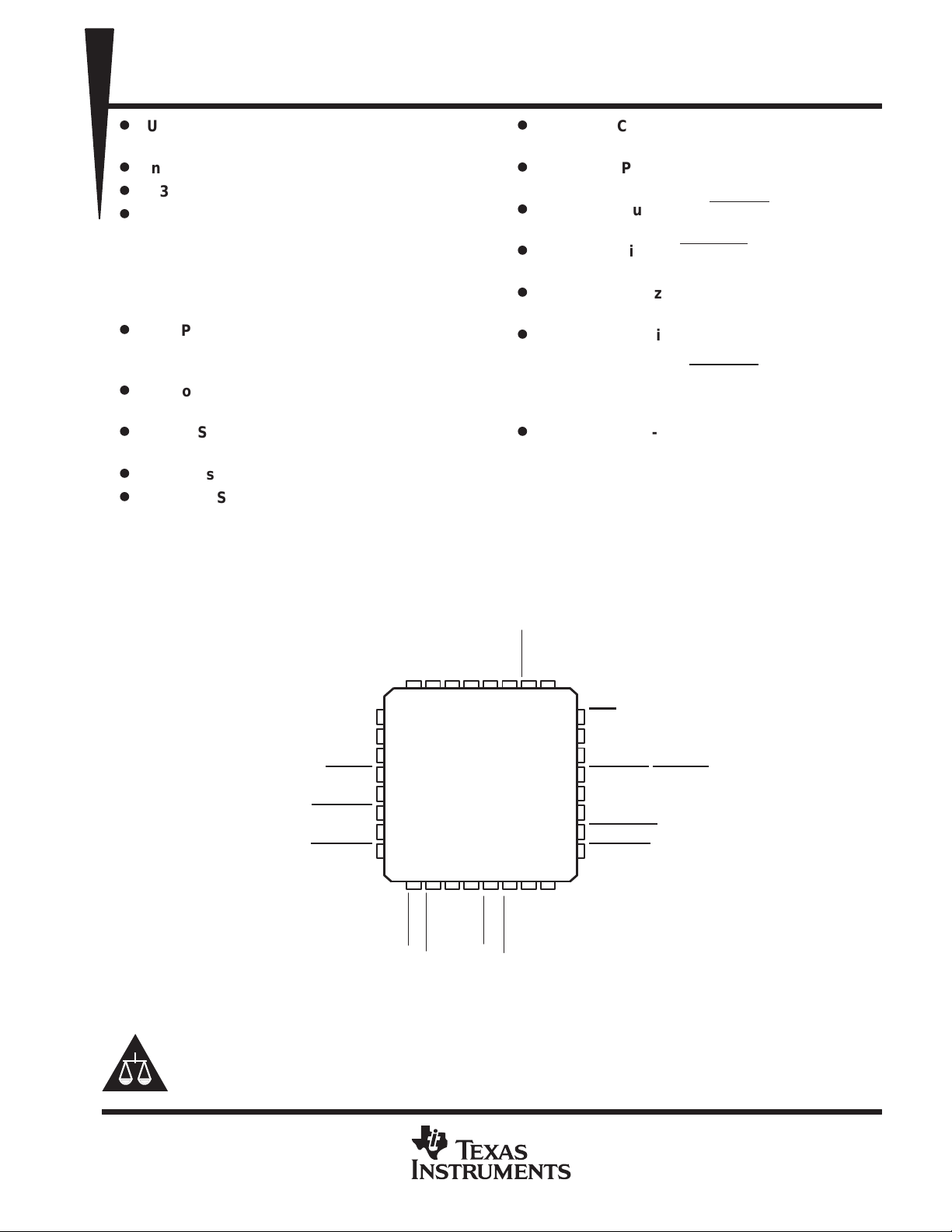
Available in 32-Pin LQFP Package With a
0.8 mm Pin Pitch (JEDEC – S-PQFP-G For
Low-Profile Quad Flat Pack)
VF PACKAGE
(TOP VIEW)
SUSPND
MODE
XTAL1/CLK48
XTAL2
GND
31 30 29 28 27
32 26
DP0
DM0
VCC
RESET
EECLK
EEDATA/GANGED
GND
BUSPWR
Please be aware that an important notice concerning availability, standard warranty, and use in critical applications of
Texas Instruments semiconductor products and disclaimers thereto appears at the end of this data sheet.
1
2
3
4
5
6
7
8
910
11 12 13
PWRON1
OVRCUR1
DM1
14 15
DP1
PWRON2
CC
DP0PUR
EXTMEM
V
25
24
23
22
21
20
19
18
17
16
DP2
DM2
OVRCUR2
NP3
NPINT1
NPINT0
OCPROT
DP3
DM3
OVRCUR3
PWRON3
/PWRSW
PRODUCTION DATA information is current as of publication date.
Products conform to specifications per the terms of Texas Instruments
standard warranty. Production processing does not necessarily include
testing of all parameters.
POST OFFICE BOX 655303 • DALLAS, TEXAS 75265
Copyright 2000, Texas Instruments Incorporated
1
Page 2

TUSB2036
2/3-PORT HUB FOR THE UNIVERSAL SERIAL BUS
WITH OPTIONAL SERIAL EEPROM INTERFACE
SLLS372 – MARCH 2000
description
The TUSB2036 hub is a 3.3-V CMOS device that provides up to three down stream ports in compliance with
the USB version 1.1 specification. Because this device is implemented with a digital state machine instead of
a microcontroller, no firmware programming is required. Fully compliant USB transceivers are integrated into
the ASIC for all upstream and downstream ports. The downstream ports support both full-speed and low-speed
devices by automatically setting the slew rate according to the speed of the device attached to the ports. The
configuration of the BUSPWR
introduction of the DP0 pull-up resistor disable pin, DP0PUR, makes it much easier to implement an on-board
bus/self-power dynamic-switching circuitry. With the new function pin, the end equipment vendor can reduce
the total board cost while adding additional product value.
The EXTMEM (Pin 26) enables or disables the optional EEPROM interface. When EXTMEM is high, the vendor
and product IDs (VID and PID) use defaults, such that the message displayed during enumeration is
Purpose USB Hub
unused. If custom VID and PID descriptors are desired, the EXTMEM must be tied low (EXTMEM = 0) and a
SGS Thompson M93C46 or equivalent EEPROM must be used to store the programmable VID, PID and
GANGED
EECLK and pin 6 as EEDATA respectively.
The TUSB2036 supports both bus-powered and self-powered modes. External power management devices
such as the TPS2044 are required to control the 5 V-power source switching (on/of f) to the downstream ports
and detect over-current condition from the downstream ports individually or ganged. Outputs from external
power devices provide over-current inputs to the TUSB2036 OVRCUR pins in case of an over-current condition,
the corresponding PWRON pins will be disabled by the TUSB2036. In the ganged mode, all PWRON signals
transitions simultaneously , and any OVRCUR input can be used. In the nonganged mode, the PWRON outputs
and OVRCUR
value. For this configuration, pin 5 and pin 6 function as the EEPROM interface signals with pin 5 as
. For this configuration, pin 6 functions as the GANGED input pin and the EECLK (Pin 5) is
inputs operate on a per port basis.
terminal selects either the bus-powered or the self-powered mode. The
General
The TUSB2036 provides the flexibility of using either a 6-MHz or a 48-MHz clock. The logic level of the MODE
terminal controls the selection of the clock source. When MODE is low, the output of the internal APLL circuitry
is selected to drive the internal core of the chip. When MODE is high, the XT AL1 input is selected as the input
clock source and the APLL circuitry is powered down and bypassed. The internal oscillator cell is also powered
down while MODE is high. For 6-MHz operation, TUSB2036 requires a 6-MHz clock signal on XT AL1 pin (with
XT AL2 for a crystal) from which its internal APLL circuitry generates a 48 MHz internal clock to sample the data
from the upstream port. For 48-MHz operation, the clock cannot be generated with a crystal, using the XT AL2
output, since the internal oscillator cell only supports fundamental frequency . If low power suspend and resume
are desired, a passive crystal or resonator must be used, although the hub supports the flexibility of using any
device that generates a 6-MHz clock. Because most oscillators cannot be stopped while power is on, their use
prohibits low-power suspend, which depends on disabling the clock. When the oscillator is used, by connecting
its output to XTAL1 terminal and leaving XTAL2 terminal open, its TTL output level can not exceed 3.6 V. If a
6 MHz oscillator is used, it must be stopped at logic low whenever SUSPND is high. For crystal or resonator
implementations, the XT AL1 terminal is the input and the XTAL2 terminal is used as the feedback path. A sample
crystal tuning circuit is shown in Figure 7.
2
POST OFFICE BOX 655303 • DALLAS, TEXAS 75265
Page 3
2/3-PORT HUB FOR THE UNIVERSAL SERIAL BUS
WITH OPTIONAL SERIAL EEPROM INTERFACE
SLLS372 – MARCH 2000
description (continued)
The hub silicon can accurately reflect the system port configuration by the NP3 and NPINT1-0 pins. When NP3
is low, the hub is configured as a 3-port hub; when it is high, the hub is configured as a 2-port hub. The NPINT1-0
pins tell the hub silicon how many ports have permanently attached devices, according to Table 1.
Table 1. System Port Configuration
TUSB2036
NPINT1-0 PORT AVAILABILITY
00 All ports are available through external USB connectors 00000000
01 Port 1 has a permanently attached device; ports 2 and 3 are externally available 00000010
10 Ports 1 and 2 have permanently attached devices; port 3 is externally available 000001 10
11 All ports have permanently attached devices NP3 high: 00000110
NP3
NPINT1-0 COMPOUND DEVICE OR NOT
00 Hub is not part of a compound device 0
01, 10, 11 Hub is part of a compound device 1
HUB DESCRIPTOR
DEVICE REMOVABLE FIELD (7–0)
low: 00001110
HUB DESCRIPTOR WITH HUB
CHARACTERISTICS FIELD BIT 2
POST OFFICE BOX 655303 • DALLAS, TEXAS 75265
3
Page 4
TUSB2036
2/3-PORT HUB FOR THE UNIVERSAL SERIAL BUS
WITH OPTIONAL SERIAL EEPROM INTERFACE
SLLS372 – MARCH 2000
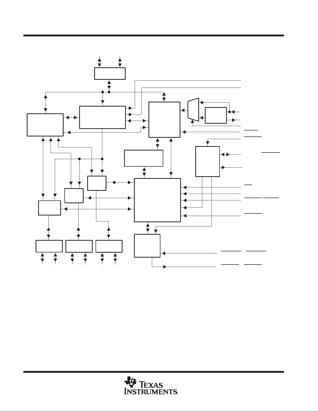
functional block diagram
DP0 DM0
12
USB
Transceiver
Suspend/Resume
Hub Repeater
Logic and
Frame Timer
SIE Interface
Logic
SIE
M
U
X
1
0
Serial
EEPROM
Interface
OSC/PLL
27
DP0PUR
32
SUSPND
30
XTAL1/CLK48
29
XTAL2
31
MODE
4
RESET
26
EXTMEM
6
EEDATA/GANGED
5
EECLK
Port 3
Logic
USB
Transceiver
20 19
Port 2
Logic
USB
Transceiver
16 15
DP2 DM2DP3 DM3
Port 1
Logic
Transceiver
12 11
DP1 DM1
USB
Hub/Device
Command
Decoder
Hub
Power
Logic
10, 14, 18
9, 13, 17
24
23, 22
OVRCUR1 – OVRCUR3
PWRON1 – PWRON3
NP3
NPINT(1–0)
21
OCPROT/PWRSW
8
BUSPWR
4
POST OFFICE BOX 655303 • DALLAS, TEXAS 75265
Page 5
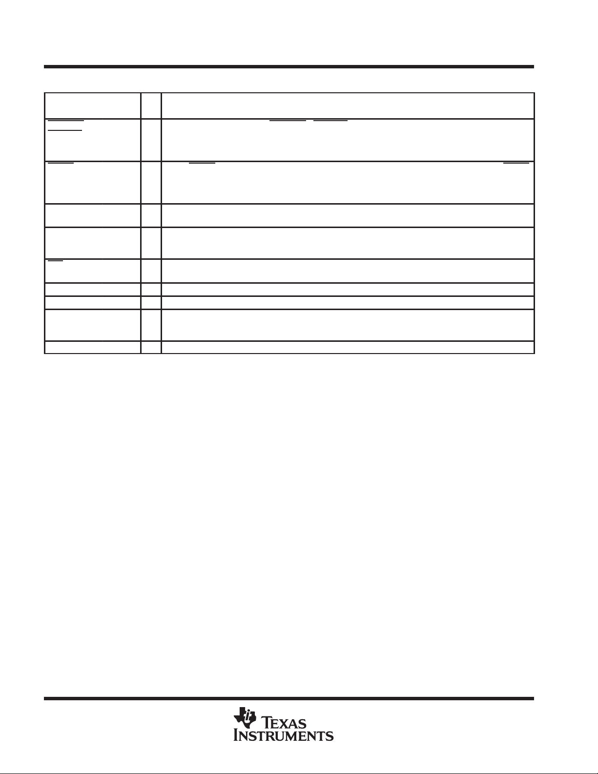
I/O
DESCRIPTION
TUSB2036
2/3-PORT HUB FOR THE UNIVERSAL SERIAL BUS
WITH OPTIONAL SERIAL EEPROM INTERFACE
SLLS372 – MARCH 2000
Terminal Functions
TERMINAL
NAME VF
BUSPWR 8 I Power source indicator. BUSPWR is an active low input that indicates whether the downstream ports source
DM0 2 I/O Root port USB differential data minus. DM0 paired with DP0 constitutes the upstream USB port.
DM1 – DM3 11, 15,19I/O USB differential data minus. DM1 – DM3 paired with DP1 – DP3 support up to three downstream USB ports.
DP0 1 I/O Root port USB differential data plus. DP0 paired with DM0 constitutes the upstream USB port.
DP0PUR 27 O Pull-up resistor connection. Whenever a system reset occurs (RESET being driven to low, but not USB reset)
DP1 – DP3 12, 16,20I/O USB differential data plus. DP1 – DP3 paired with DM1 – DM3 support up to three downstream USB ports.
their power from the USB cable or a local power supply. For the bus-power mode, this pin should be pulled
low, and for the self-powered mode, this pin should be pulled to 3.3 V. Input must not change dynamically
during operation.
or any logic level change on BUSPWR terminal, DP0PUR output goes to inactive Low until the internal counter
reaches a 3 ms time period. After the counter expires, DP0PUR is driven to the VCC (3.3 V) level thereafter
until the next system reset event or BUSPWR
logic level change.
EECLK 5 O EEPROM serial clock. When EXTMEM is high, the EEPROM interface is disabled. The EECLK pin is disabled
EEDATA/
GANGED
EXTMEM 26 I EEPROM read enable. When EXTMEM is high, the serial EEPROM interface of the device is disabled. When
GND 7, 28 Ground. GND terminals must be tied to ground for proper operation.
OCPROT/
PWRSW
OVRCUR1 –
OVRCUR3
NOTES: 1. If the hub is implemented to be bus-powered (via BUSPWR tying to GND):
2. If the hub is implemented to be self-powered (via BUSPWR
6 I/O EEPROM serial data/power management mode indicator. When EXTMEM is high, EEDATA/GANGED
21 I Overcurrent Protection for bus-powered hub (active low). /Power Switching for self-powered hub (active low).
10, 14,18I overcurrent input. OVRCUR1 – OVRCUR3 are active low. For per-port overcurrent detection, one overcurrent
– TUSB2036 reports to the host that the hub end-product downstream ports are power-switched (this is required by the USB 1.1
Specification). Hub end product vendor has to ensure the actual end product implementation meets this specification requirement.
– Pin 21 acts as overcurrent protection (OCPROT
protection implementation is reported through the wHubCharacteristics. D4-bit in the hub descriptor.
– When OCPROT
wHubCharacteristics. D4-bit is set to 0.
– When OCPROT
and the wHubCharacteristics. D4-bit is set to 1.
– TUSB2036 reports to the host that the hub end-product provides overcurrent protection to the downstream ports (this is required
by the USB 1.1 Specification). Hub end product vendor has to ensure the actual end-product implementation meets this
specification requirement.
– Pin 21 acts as power switching (PWRSW) implementation indication pin for the self-powered hub. The power switching
implementation is reported through the bPwrOn2PwrGood field in the hub descriptor.
– When PWRSW
ports and the bPwrOn2PwrGood is set to 50 units (100 ms).
– When PWRSW
downstream ports and the bPwrOn2PwrGood is set to 0 units (0 ms).
and should be left floating (unconnected). When EXTMEM
to the EEPROM with a 100 µA internal pulldown.
selects between gang and per-port power overcurrent detection for the downstream ports. When EXTMEM
is low, EEDATA/GANGED acts as a serial data I/O for the EEPROM and is internally pulled down with a
100 µA pulldown. This standard TTL input must not change dynamically during operation.
EXTMEM
respectively.
The pin has a different meaning for the bus or self-powered hub. If the pin is logic-high the internal pull-down
is disabled. (see Notes 1 and 2 ).
input is available for each of the three downstream ports. In the ganged mode, any OVRCUR
used and all OVRCUR
logic. OVRCUR3
is low, the TUSB2036 reports to the host that the hub end-product has port power switching at the downstream
is high, the TUSB2036 reports to the host that the hub end-product does not have port power switching at the
is low, terminals 5 and 6 are configured as the clock and data pins of the serial EEPROM interface,
pins should be tied together. OVRCUR pins are active low inputs with noise filtering
has an internal pull-up that can be enabled for the 2-port operation.
) implementation indication pin for the bus-powered hub. The overcurrent
is low, the TUSB2036 reports to the host that the hub end-product provides overcurrent protection and the
is high, the TUSB2036 reports to the host that the hub end-product does not provide overcurrent protection
tying to 3.3-V VCC),:
is low, EECLK acts as a 3-state serial clock output
input may be
POST OFFICE BOX 655303 • DALLAS, TEXAS 75265
5
Page 6
TUSB2036
I/O
DESCRIPTION
2/3-PORT HUB FOR THE UNIVERSAL SERIAL BUS
WITH OPTIONAL SERIAL EEPROM INTERFACE
SLLS372 – MARCH 2000
Terminal Functions (Continued)
TERMINAL
NAME VF
PWRON1 –
PWRON3
RESET 4 I Reset. RESET is an active low TTL input with hysteresis and must be asserted at power up. When RESET
SUSPND 32 O Suspend status. SUSPND is an active high output available for external logic power-down operations. During
MODE 31 I Mode select. When MODE is low, the APLL output clock is selected as the clock source to drive the internal
NP3 24 I Number of ports is 3. Active low input. A logic 0 configures the system to use 3 ports. A logic 1, configures
NPINT1–0 23, 22 I Number of ports internal to hub system, which are permanently attached (see Table 1)
VCC 3, 25 3.3-V supply voltage
XTAL1/CLK48 30 I Crystal 1/48-MHz Clock Input. When MODE is low, XTAL1/CLK48 is a 6-MHz crystal input with 50% duty
XTAL2 29 O Crystal 2. XTAL2 is a 6-MHz crystal output. This terminal should be left open when using an oscillator.
9, 13,17O Power-on/-off control signals. PWRON1 – PWRON3 are active low, push-pull outputs. Push-pull outputs
eliminate the pullup resistors which open-drain outputs require. However, the external power switches that
connect to these pins must be able to operate with 3.3-V inputs because these outputs cannot drive 5-V
signals.
is asserted, all logic is initialized. Generally, a reset with a pulse width between 100 µs and 1 ms is
recommended after 3.3-V VCC reaching its 90%. The clock signal must be active during the last 60 µs of the
reset window.
the suspend mode, SUSPND is high. SUSPND is low for normal operation.
core of the chip and 6-MHz crystal or oscillator can be used. When MODE is high, the clock on XTAL1/CLK48
is selected as the clock source and 48-MHz oscillator or other on-board clock source can be used.
the system to use 2 ports.
cycle. An internal APLL generates the 48-MHz and 12-MHz clocks used internally by the ASIC logic. When
MODE is high, XTAL1/CLK48 acts as the input of the 48 MHz clock and the internal APLL logic is bypassed.
6
POST OFFICE BOX 655303 • DALLAS, TEXAS 75265
Page 7

TUSB2036
2/3-PORT HUB FOR THE UNIVERSAL SERIAL BUS
WITH OPTIONAL SERIAL EEPROM INTERFACE
SLLS372 – MARCH 2000
absolute maximum ratings over operating free-air temperature range (unless otherwise noted)
Supply voltage range, VCC (see Note 1) –0.5 V to 3.6 V. . . . . . . . . . . . . . . . . . . . . . . . . . . . . . . . . . . . . . . . . . . . .
Input voltage range, VI –0.5 V to VCC + 0.5 V. . . . . . . . . . . . . . . . . . . . . . . . . . . . . . . . . . . . . . . . . . . . . . . . . . . . . .
Output voltage range, V
–0.5 V to VCC + 0.5 V. . . . . . . . . . . . . . . . . . . . . . . . . . . . . . . . . . . . . . . . . . . . . . . . . . . .
O
Input clamp current, IIK, (VI < 0 V or VI > VCC) ±20 mA. . . . . . . . . . . . . . . . . . . . . . . . . . . . . . . . . . . . . . . . . . . . .
Output clamp current, IOK, (VO < 0 V or V
Storage temperature range, T
–65°C to 150°C. . . . . . . . . . . . . . . . . . . . . . . . . . . . . . . . . . . . . . . . . . . . . . . . . . .
stg
> VCC) ±20 mA. . . . . . . . . . . . . . . . . . . . . . . . . . . . . . . . . . . . . . . . .
O
Operating free-air temperature range, TA 0°C to 70°C. . . . . . . . . . . . . . . . . . . . . . . . . . . . . . . . . . . . . . . . . . . . . .
†
Stresses beyond those listed under “absolute maximum ratings” may cause permanent damage to the device. These are stress ratings only, and
functional operation of the device at these or any other conditions beyond those indicated under “recommended operating conditions” is not
implied. Exposure to absolute-maximum-rated conditions for extended periods may affect device reliability.
NOTE 3: All voltage levels are with respect to GND.
recommended operating conditions
MIN NOM MAX UNIT
Supply voltage, V
Input voltage, TTL/LVCMOS, V
Output voltage, TTL/LVCMOS, V
High-level input voltage, signal-ended receiver, V
Low-level input voltage, signal-ended receiver, V
High-level input voltage, TTL/LVCMOS, V
Low-level input voltage, TTL/LVCMOS, V
Operating free-air temperature, T
External series, differential driver resistor, R
Operating (dc differential driver) high-speed mode, f
Operating (dc differential driver) low-speed mode, f
Common mode, input range, differential receiver , V
Input transition times, tt, TTL/LVCMOS 0 25 ns
Junction temperature range, T
CC
I
O
IH(REC)
IL(REC)
IH(TTL)
IL(TTL)
A
(DRV)
(OPRH)
(OPRL)
(ICR)
J
3 3.3 3.6 V
0 V
0 V
2 V
2 V
0 0.8 V
0 70 °C
22 (–5%) 22 (+5%) Ω
0.8 2.5 V
0 115 °C
CC
CC
CC
0.8 V
CC
12 Mb/s
1.5 Mb/s
V
V
V
V
†
POST OFFICE BOX 655303 • DALLAS, TEXAS 75265
7
Page 8

TUSB2036
USB data lines
USB data lines
V
Positi
V
N
V
I
(V
VT–)
IOZHigh-impedance output current
ICCInput supply current
2/3-PORT HUB FOR THE UNIVERSAL SERIAL BUS
WITH OPTIONAL SERIAL EEPROM INTERFACE
SLLS372 – MARCH 2000
electrical characteristics over recommended ranges of operating free-air temperature and supply
voltage (unless otherwise noted)
PARAMETER TEST CONDITIONS MIN MAX UNIT
V
OH
V
OL
IT+
IT–
hys
I
IL
I
IH
z
o(DRV)
V
ID
†
Applies for input buffers with hysteresis
‡
Applies for open drain buffers
High-level output voltage
Low-level output voltage
ve input threshold voltage
egative-input threshold voltage
nput hysteresis†
p
Low-level input current TTL/LVCMOS VI = GND –1 µA
High-level input current TTL/LVCMOS VI = V
Driver output impedance USB data lines Static VOH or V
Differential input voltage USB data lines 0.8 V ≤ V
p
pp
T+
p
–
TTL/LVCMOS IOH = –4 mA VCC –
R
= 15 kΩ, to GND 2.8
(DRV)
IOH = –12 mA (without R
TTL/LVCMOS IOL = 4 mA 0.5
R
= 1.5 k Ω to 3.6 V 0.3
(DRV)
IOL = 12 mA (without R
TTL/LVCMOS 1.8 V
Single-ended
TTL/LVCMOS 0.8 V
Single-ended
TTL/LVCMOS 0.3 0.7 V
Single-ended 0.8 V ≤ V
TTL/LVCMOS V = VCC or GND‡ ±10 µA
USB data lines 0 V ≤ VO ≤ V
0.8 V ≤ V
0.8 V ≤ V
Normal operation 40 mA
Suspend mode 1 µA
≤ 2.5 V 1.8 V
ICR
≤ 2.5 V 1 V
ICR
≤ 2.5 V 300 500 mV
ICR
CC
CC
OL
≤ 2.5 V 0.2 V
ICR
) VCC –
(DRV)
) 0.5
(DRV)
0.5
V
0.5
V
±10 µA
1 µA
7.1 19.9 Ω
differential driver switching characteristics over recommended ranges of operating free-air
temperature and supply voltage, C
full speed mode
PARAMETER TEST CONDITIONS MIN MAX UNIT
t
r
t
f
t
(RFM)
V
O(CRS)
§
Characterized only. Limits approved by design and are not production tested
low speed mode
t
r
t
f
t
(RFM)
V
O(CRS)
§
Characterized only. Limits approved by design and are not production tested
Transition rise time for DPor DM See Figure 1 and Figure 2 4 20 ns
Transition fall time for DPor DM See Figure 1 and Figure 2 4 20 ns
Rise/fall time matching
Signal crossover output voltage
PARAMETER TEST CONDITIONS MIN MAX UNIT
Transition rise time for DPor DM
Transition fall time for DPor DM
Rise/fall time matching
Signal crossover output voltage
§
§
= 50 pF (unless otherwise noted)
L
(tr/tf) x 100 90% 110%
§
§
CL = 200 pF to 600 pF, See Figure 1 and Figure 2 75 300 ns
§
§
CL = 200 pF to 600 pF, See Figure 1 and Figure 2 75 300 ns
(tr/tf) x 100 80% 120%
CL = 200 pF to 600 pF 1.3 2.0 V
1.3 2.0 V
8
POST OFFICE BOX 655303 • DALLAS, TEXAS 75265
Page 9

TUSB2036
2/3-PORT HUB FOR THE UNIVERSAL SERIAL BUS
WITH OPTIONAL SERIAL EEPROM INTERFACE
SLLS372 – MARCH 2000
DP
22 Ω
DM
22 Ω
Figure 1. Differential Driver Switching Load
t
f
DM
DP
NOTE: The tr/tf ratio is measured as t
90%
10%
90%
10%
t
r
Figure 2. Differential Driver Timing Waveforms
1.5
Characterization
Measurement Point
15 kΩ
15 kΩ
r(DP)/tf(DM)
and t
C
L
C
L
90%
10%
r(DM)/tf(DP)
V(
at each crossover point.
TERM)
Full
Low
90%
10%
t
f
t
r
= V
1.5 kΩ
CC
V
V
OH
OL
1.3
1
0.5
0.2
– Differential Receiver Input Sensitivity – V
ID
V
0
012
0.8
V
– Common Mode Input Range – V
ICR
34
2.5
3.6
Figure 3. Differential Receiver Input Sensitivity vs Common Mode Input Range
V
V
V
0 V
CC
IH
IL
IT–
V
hys
Logic high
V
IT+
V
Logic low
Figure 4. Single-Ended Receiver Input Signal Parameter Definitions
POST OFFICE BOX 655303 • DALLAS, TEXAS 75265
9
Page 10

TUSB2036
2/3-PORT HUB FOR THE UNIVERSAL SERIAL BUS
WITH OPTIONAL SERIAL EEPROM INTERFACE
SLLS372 – MARCH 2000
APPLICATION INFORMATION
A major advantage of USB is the ability to connect 127 functions configured in up to six logical layers (tiers) to
a single personal computer (see Figure 5).
PC
With Root Hub
Monitor
Modem Telephone
Printer
With 4-Port Hub
(Self-Powered)
Scanner
Digital
Scanner
Left
Speaker
Keyboard
With 4-Port Hub
(Bus-Powered)
Mouse
With 4-Port Hub (Self-Powered)
Right
Speaker
Figure 5. USB Tiered Configuration Example
Another advantage of USB is that all peripherals are connected using a standardized four-wire cable that
provides both communication and power distribution. The power configurations are bus-powered and
self-powered modes. The maximum current that may be drawn from the USB 5-V line during power up is 100
mA. For the bus-powered mode, a hub can draw a maximum of 500 mA from the 5-V line of the USB cable. A
bus-powered hub must always be connected downstream to a self-powered hub unless it is the only hub
connected to the PC and there are no high-powered functions connected downstream. In the self-powered
mode, the hub is connected to an external power supply and can supply up to 500 mA to each downstream port.
High-powered functions may draw a maximum of 500 mA from each downstream port and may only be
connected downstream to self-powered hubs. Per the USB specification, in the bus-powered mode, each
downstream port can provide a maximum of 100 mA of current, and in the self-powered mode, each
downstream port can provide a maximum of 500 mA of current.
Both bus-powered and self-powered hubs require overcurrent protection for all downstream ports. The two
types of protection are individual port management (individual port basis) or ganged port management (multiple
port basis). Individual port management requires power management devices for each individual downstream
port, but adds robustness to the USB system because, in the event of an overcurrent condition, the USB host
only powers down the port that has the condition. The ganged configuration uses fewer power management
devices and thus has lower system costs, but in the event of an overcurrent condition on any of the downstream
ports, all the ganged ports are disabled by the USB host.
Using a combination of the BUSPWR
and EEDATA/GANGED inputs, the TUSB2036 supports four modes of
power management: bus-powered hub with either individual port power management or ganged port power
management, and the self-powered hub with either individual port power management or ganged port power
management. Texas Instruments supplies the complete hub solution because we offer this TUSB2036, the
TUSB2043/TUSB2046 (4-port), the TUSB2077A (7-port) and the TUSB2140B (4-port with I
2
C) hubs along with
the power management chips needed to implement a fully USB Specification 1.1 compliant system.
10
POST OFFICE BOX 655303 • DALLAS, TEXAS 75265
Page 11

2/3-PORT HUB FOR THE UNIVERSAL SERIAL BUS
WITH OPTIONAL SERIAL EEPROM INTERFACE
SLLS372 – MARCH 2000
APPLICATION INFORMATION
USB design notes
The following sections provide block diagram examples of how to implement the TUSB2036 device. Please
note, even though no resistors are shown, pullup, pulldown and series resistors must still be used to properly
implement this device.
Figure 6 is a block diagram example of how to connect the external EEPROM if a custom product ID and vendor
ID are desired.
Figure 7 is an example of how to generate the 6-MHz clock signal. Figure 8 shows the EEPROM read operation
timing diagram. Figures 9, 10, and 11 illustrate how to connect the TUSB2036 device for dif ferent power source
and port power management combinations.
TUSB2036 USB Hub
3.3 V
Power-On Reset
EEPROM
6
ORG
8
V
CC
5
V
SS
S
System
D
Q
C
6-MHz Clock
Signal
3
1 kΩ
4
2
(3-Port Configuration)
30
XTAL1/CLK48
29
XTAL2
4
RESET
26
EXTMEM
1
DP0
2
DM0
6
EEDATA
5
EECLK
MODE
V
OCPROT/
PWRSW
GND
DP1 – DP3
DM1 – DM4
OVRCUR1
OVRCUR3
PWRON1 –
PWRON3
NPINT1
NPINT0
CC
NP3
–
3, 25
24
21
7, 28
12, 16, 20
11, 15, 19
10, 14, 18
9, 13, 17
23
22
5 V GND
Regulator
Power
Switching
Bus or Local Power
4
4
4
GND
4
V
bus
USB Data lines
and Power to
Downstream
Ports
TUSB2036
1
Figure 6. Typical Application of the TUSB2036 USB Hub
C
L
XTAL1 XTAL2
R
d
C2C1
NOTE A: Figure 7 assumes a 6 MHz fundamental crystal that is parallel loaded. The component values of C1, C2 and Rd were determined
using a crystal from Fox Electronics– part number HC49U–6.00MHz30\50\0 ±70\20 which means ±30 ppm at 25°C and 50 ppm from
0°C to 70°C. The characteristics for the crystal are load capacitance (CL) of 20 pF , maximum shunt capacitance (Co) of 7 pF and the
maximum ESR of 50 Ω. In order to insure enough negative resistance, use C1 = C2 = 27 pF . The resistor Rd is used to trim the gain,
and Rd = 1.5 kΩ
is recommended.
Figure 7. Crystal Tuning Circuit
POST OFFICE BOX 655303 • DALLAS, TEXAS 75265
11
Page 12

TUSB2036
2/3-PORT HUB FOR THE UNIVERSAL SERIAL BUS
WITH OPTIONAL SERIAL EEPROM INTERFACE
SLLS372 – MARCH 2000
APPLICATION INFORMATION
programming the EEPROM
An SGS Thompson M93C46 EEPROM or equivalent is used for storing the programmable VID and PID. When
the EEPROM interface is enabled (EXTMEM
inside the TUSB2036. The internal pulldowns are disabled when the EEPROM interface is disabled
(EXTMEM
= 1).
The EEPROM is programmed with the three 16-bit locations as shown in Table 1. Connecting pin 6 of the
EEPROM high (ORG = 1) organizes the EEPROM memory into 64×16 bit words.
Table 2. EEPROM Memory Map
ADDRESS D15 D14 D13 D12–D8 D7–D0
00000 0
00001 VID High-byte VID Low-byte
00010 PID High-byte PID Low-byte
The D and Q signals of the EEPROM must be tied together using a 1 kΩ resistor with the common I/O operations
forming a single-wire bus. After system power-on reset, the TUSB2036 performs a one-time access read
operation from the EEPROM if the EXTMEM
connected to the system power-on reset. Initially, the EEDATA pin will be driven by the TUSB2036 to send a
start bit (1), which is followed by the read instruction (10) and the starting-word address (00000). Once the read
instruction is received, the instruction and address are decoded by the EEPROM, which then sends the data
to the output shift register. At this point, the hub stops driving the EEDATA pin and the EEPROM starts driving.
A dummy (0) bit is then output and the first three 16-bit words in the EEPROM are output with the most significant
bit (MSB) first.
= 0), the EECLK and EEDA TA are internally pulled down (100 µA)
GANGED 00000 00000 00000000
XXXXXXXX
pin is pulled low and the chip select(s) of the EEPROM is
The output data changes are triggered by the rising edge of the clock provided by the TUSB2036 on the EECLK
pin. The
SGS-Thompson M93C46
EEPROM is recommended because it advances to the next memory location
by automatically incrementing the address internally. Any EEPROM used must have the automatic internal
address advance function. After reading the three words of data from the EEPROM, the TUSB2036 puts the
EEPROM interface into a high-impedance condition (pulled down internally) to allow other logic to share the
EEPROM. The EEPROM read operation is summarized in Figure 8. For more details on EEPROM operation,
refer to
SGS-Thompson Microelectronics M93C46 Serial Microwire Bus EEPROM
data sheet.
12
POST OFFICE BOX 655303 • DALLAS, TEXAS 75265
Page 13

TUSB2036
2/3-PORT HUB FOR THE UNIVERSAL SERIAL BUS
WITH OPTIONAL SERIAL EEPROM INTERFACE
3-Stated
Pulldown
With Internal
MSB of
Fourth Word
LSB of
Third Word
Other
Data Bits
EEPROM Driving Data LineHub Driving Data Line
SLLS372 – MARCH 2000
D15 D14 D0 XX
6 Bit Address (000000)Start Read OP Code(10) 48 Data Bits Don’t Care
First Word
MSB of The
Bit
A0 Dummy
Bits
Other
Address
A5 A1
Figure 8. EEPROM Read Operation Timing Diagram
S
POST OFFICE BOX 655303 DALLAS, TEXAS 75265
C
D
• 13
Page 14

TUSB2036
2/3-PORT HUB FOR THE UNIVERSAL SERIAL BUS
WITH OPTIONAL SERIAL EEPROM INTERFACE
SLLS372 – MARCH 2000
APPLICATION INFORMATION
bus-powered hub, ganged port-power management
When used in bus-powered mode, the TUSB2036 supports up to three downstream ports by controlling a
TPS2041 device which is capable of supplying 100 mA of current to each downstream port. Bus-powered hubs
must implement power switching to ensure current demand is held below 100 mA when the hub is hot-plugged
into the system. Utilizing the TPS2041 for ganged power management provides overcurrent protection for the
downstream ports. The SN75240 transient suppressors reduce inrush current and voltage spikes on the data
lines. The OVRCUR
signals should be tied together for a ganged operation.
TUSB2036
3-Port Configuration With
no Permanently Attached Devices.
Upstream
Port
D +
D –
5 V
GND
SN75240
A
C
B
D
4.7 µF
0.1 µF
6-MHz Clock
Signal
System
Power-On Reset
1.5 kΩ
†
3.3 V LDO
5 V
3.3 V
GND
3.3 V
§
4.7 µF
DP0PUR
EEDATA/GANGED
DP0
DM0
OCPROT/PWRSW
V
CC
XTAL1/CLK48
XTAL2
MODE
EXTMEM
RESET
GND
BUSPWR
DP1
DM1
DP2
DM2
NP3
NPINT1
NPINT0
DP3
DM3
PWRON1
PWRON2
PWRON3
OVRCUR1
OVRCUR2
OVRCUR3
15 kΩ
15 kΩ
15 kΩ
15 kΩ
SN75240
SN75240
TPS2041
EN IN
OUT
OUT
OUT
OC
ABC
ABC
†
IN
Downstream
Ports
D +
Ferrite Beads
D
†
15 kΩ
15 kΩ
D
†
1 µF
100 µF
Ferrite Beads
100 µF
Ferrite Beads
100 µF
D –
GND
5 V
‡
D +
D –
GND
5 V
‡
D +
D –
GND
5 V
‡
†
TPS2041 and SN75240 are Texas Instruments devices.
‡
120 µF per hub is the minimum required per the USB specification, version 1.1. However , TI recommends a 100 µF low ESR tantalum capacitor
per port for immunity to voltage droop.
§
LDO is a 5 V to 3.3 V voltage regulator
Figure 9. TUSB2036 Bus-Powered Hub, Ganged Port-Power Management Application
14
POST OFFICE BOX 655303 • DALLAS, TEXAS 75265
Page 15

TUSB2036
2/3-PORT HUB FOR THE UNIVERSAL SERIAL BUS
WITH OPTIONAL SERIAL EEPROM INTERFACE
SLLS372 – MARCH 2000
APPLICATION INFORMATION
bus-powered hub with a permanently attached high speed device, ganged port-power
management
Upstream
Port
D +
D –
5 V
GND
SN75240
A
C
B
D
4.7 µF
0.1 µF
6-MHz Clock
Signal
System
Power-On Reset
1.5 kΩ
†
3.3 V LDO
5 V
3.3 V
GND
3.3 V
§
4.7 µF
TUSB2036
DP0PUR
DP0
DM0
EEDATA/GANGED
V
CC
MODE
XTAL1/CLK48
XTAL2
EXTMEM
RESET
GND
OCPROT/PWRSW
DP1
DM1
BUSPWR
DP2
DM2
DP3
DM3
PWRON1
PWRON2
PWRON3
NP3
NPINT1
NPINT0
OVRCUR1
OVRCUR2
OVRCUR3
15 kΩ
15 kΩ
3.3 V
15 kΩ
15 kΩ
3.3 V
EN1
EN2
EN3
EN4
OC1
OC2
OC3
OC4
SN75240
TPS2044
OUT1
OUT2
OUT3
OUT4
IN1
IN2
ABC
D
ABC
SN75240
†
†
D
†
0.1 µF
3.3 V
15 kΩ
15 kΩ
15 kΩ
15 kΩ
Permanently Attached
1.5 k
High Speed Device
100 µF
D +
D –
GND
5 V
‡
Downstream
Ports
D +
D –
GND
5 V
‡
100 µF
D +
D –
GND
5 V
‡
100 µF
†
TPS2042 and SN75240 are Texas Instruments devices. Two TPS2042 devices can be substituted for
the TPS2044.
‡
120 µF per hub is the minimum required per the USB specification, version 1.1. However, TI recommends a 100 µF low ESR tantalum capacitor
per port for immunity to voltage droop.
§
LDO is a 5 V to 3.3 V voltage regulator
Figure 10. TUSB2036 Bus-Powered Hub With a Permanently Attached High Speed Device, Individual
Port-Power Management Application
POST OFFICE BOX 655303 • DALLAS, TEXAS 75265
15
Page 16

TUSB2036
2/3-PORT HUB FOR THE UNIVERSAL SERIAL BUS
WITH OPTIONAL SERIAL EEPROM INTERFACE
SLLS372 – MARCH 2000
APPLICATION INFORMATION
self-powered hub, ganged port-power management
The TUSB2036 can also be implemented for ganged port-power management in a self-powered configuration.
The implementation is very similar to the bus-powered example with the exception that a self-powered port
supplies 500 mA of current to each downstream port. The overcurrent protection can be provided by a TPS2044
quad device or a TPS2024 single power switch.
Upstream
Port
D +
D –
5 V
GND
SN75240
A
B
4.7 µF
0.1 µF
6-MHz Clock
Signal
†
C
D
3.3 V LDO
5 V
3.3 V
GND
1.5 kΩ
§
4.7 µF
TUSB2036
DP0PUR
EEDATA/GANGED
DP0
DM0
V
CC
MODE
XTAL1/CLK48
XTAL2
BUSPWR
DP1
DM1
DP2
DM2
DP3
DM3
3.3 V
15 kΩ
15 kΩ
15 kΩ
15 kΩ
ABC
D
SN75240
†
SN75240
ABC
15 kΩ
D
Ferrite Beads
15 kΩ
100 µF
Ferrite Beads
†
Downstream
Ports
D +
D –
GND
5 V
‡
D +
D –
GND
5 V
3.3 V
System
Power-On Reset
†
TPS2044, TPS2042, and SN75240 are Texas Instruments devices.
EXTMEM
RESET
GND
NP3
NPINT1
NPINT0
OCPROT/PWRSW
PWRON1
PWRON2
PWRON3
OVRCUR1
OVRCUR2
OVRCUR3
TPS2044
EN2
EN3
EN4
OC1
OC2
OC3
OC4
OUT1
OUT2
OUT3
OUT4
IN1EN1
IN2
†
0.1 µF
Ferrite Beads
5 V Board Power
100 µF
100 µF
Supply
‡
D +
D –
GND
5 V
‡
The TPS2024 can be substituted for the TPS2044.
‡
120 µF per hub is the minimum required per the USB specification, version 1.1. However, TI recommends a 100 µF low ESR tantalum capacitor
per port for immunity to voltage droop.
§
LDO is a 5 V to 3.3 V voltage regulator
Figure 11. TUSB2036 Self-Powered Hub, Ganged Port-Power Management Application
16
POST OFFICE BOX 655303 • DALLAS, TEXAS 75265
Page 17

2/3-PORT HUB FOR THE UNIVERSAL SERIAL BUS
WITH OPTIONAL SERIAL EEPROM INTERFACE
SLLS372 – MARCH 2000
APPLICATION INFORMATION
self-powered hub, individual port-power management (continued)
In a self-powered configuration, the TUSB2036 can be implemented for individual port-power management
when used with the TPS2044 because it is capable of supplying 500 mA of current to each downstream port
and can provide current limiting on a per port basis. When the hub detects a fault on a downstream port, power
is removed from only the port with the fault and the remaining ports continue to operate normally . Self-powered
hubs are required to implement overcurrent protection and report overcurrent conditions. The SN75240
transient suppressors reduce inrush current and voltage spikes on the data lines.
TUSB2036
Upstream
Port
D +
D –
5 V
GND
4.7 µF
0.1 µF
SN75240
A
C
B
D
1.5 kΩ
†
3.3 V LDO
5 V
3.3 V
GND
§
4.7 µF
DP0PUR
DP0
DM0
V
CC
MODE
DP1
DM1
BUSPWR
EEDATA/GANGED
DP2
DM2
DP3
DM3
3.3 V
15 kΩ
15 kΩ
15 kΩ
15 kΩ
ABC
SN75240
SN75240
D
ABC
15 kΩ
†
D
†
15 kΩ
TUSB2036
Downstream
Ports
D +
D –
GND
5 V
‡
100 µF
D +
D –
GND
5 V
‡
Supply
100 µF
100 µF
D +
D –
GND
5 V
‡
XTAL1/CLK48
†
6-MHz Clock
Signal
XTAL2
3.3 V
System
Power-On Reset
†
TPS2042 and SN75240 are Texas Instruments devices. Two TPS2042 devices can be substituted for
EXTMEM
RESET
GND
OCPROT
PWRON1
PWRON2
PWRON3
NP3
NPINT1
NPINT0
OVRCUR1
OVRCUR2
OVRCUR3
/PWRSW
TPS2044
EN1
EN2
EN3
EN4
OUT1
OUT2
OUT3
OUT4
OC1
OC2
OC3
OC4
IN1
IN2
0.1 µF
5-V Board Power
the TPS2044.
‡
120 µF per hub is the minimum required per the USB specification, version 1.1. However, TI recommends a 100 µF low ESR tantalum capacitor
per port for immunity to voltage droop.
§
LDO is a 5 V to 3.3 V voltage regulator
Figure 12. TUSB2036 Self-Powered Hub, Individual Port-Power Management Application
POST OFFICE BOX 655303 • DALLAS, TEXAS 75265
17
Page 18

TUSB2036
2/3-PORT HUB FOR THE UNIVERSAL SERIAL BUS
WITH OPTIONAL SERIAL EEPROM INTERFACE
SLLS372 – MARCH 2000
MECHANICAL DATA
VF (S-PQFP-G32) PLASTIC QUAD FLATPACK
25
32
0,80
1,45
1,35
24
0,45
0,30
17
16
9
1
5,60 TYP
7,20
SQ
6,80
9,20
SQ
8,80
8
0,22
M
0,05 MIN
0,13 NOM
Gage Plane
0,25
0°–7°
1,60 MAX
NOTES: A. All linear dimensions are in millimeters.
B. This drawing is subject to change without notice.
C. Falls within JEDEC MS-026
Seating Plane
0,10
0,75
0,45
4040172/C 10/96
18
POST OFFICE BOX 655303 • DALLAS, TEXAS 75265
Page 19

TUSB2036
2/3-PORT HUB FOR THE UNIVERSAL SERIAL BUS
WITH OPTIONAL SERIAL EEPROM INTERFACE
SLLS372 – MARCH 2000
(This page has been left blank intentionally.)
POST OFFICE BOX 655303 • DALLAS, TEXAS 75265
19
Page 20

IMPORTANT NOTICE
T exas Instruments and its subsidiaries (TI) reserve the right to make changes to their products or to discontinue
any product or service without notice, and advise customers to obtain the latest version of relevant information
to verify, before placing orders, that information being relied on is current and complete. All products are sold
subject to the terms and conditions of sale supplied at the time of order acknowledgement, including those
pertaining to warranty, patent infringement, and limitation of liability.
TI warrants performance of its semiconductor products to the specifications applicable at the time of sale in
accordance with TI’s standard warranty. Testing and other quality control techniques are utilized to the extent
TI deems necessary to support this warranty . Specific testing of all parameters of each device is not necessarily
performed, except those mandated by government requirements.
CERTAIN APPLICATIONS USING SEMICONDUCTOR PRODUCTS MAY INVOLVE POTENTIAL RISKS OF
DEATH, PERSONAL INJURY, OR SEVERE PROPERTY OR ENVIRONMENTAL DAMAGE (“CRITICAL
APPLICATIONS”). TI SEMICONDUCTOR PRODUCTS ARE NOT DESIGNED, AUTHORIZED, OR
WARRANTED TO BE SUITABLE FOR USE IN LIFE-SUPPORT DEVICES OR SYSTEMS OR OTHER
CRITICAL APPLICA TIONS. INCLUSION OF TI PRODUCTS IN SUCH APPLICATIONS IS UNDERST OOD TO
BE FULLY AT THE CUSTOMER’S RISK.
In order to minimize risks associated with the customer’s applications, adequate design and operating
safeguards must be provided by the customer to minimize inherent or procedural hazards.
TI assumes no liability for applications assistance or customer product design. TI does not warrant or represent
that any license, either express or implied, is granted under any patent right, copyright, mask work right, or other
intellectual property right of TI covering or relating to any combination, machine, or process in which such
semiconductor products or services might be or are used. TI’s publication of information regarding any third
party’s products or services does not constitute TI’s approval, warranty or endorsement thereof.
Copyright 2000, Texas Instruments Incorporated
 Loading...