

Page 1
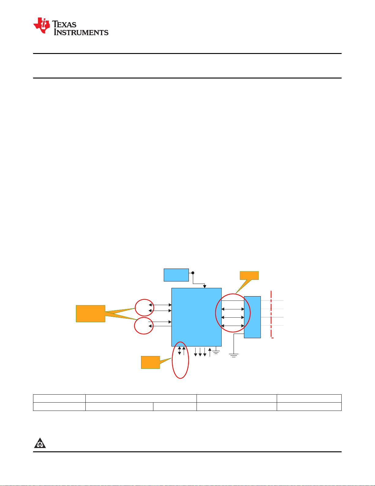
USB CONNECTOR
BATTERY
VBAT
RxD
TxD
DP_HT
DM_HT
MICMICMICMIC
ID_CON
DP_CON
VBUS
DM_CON
TSU6111
I2C_SDA
INTB
BOOT
JIG
I2C_SCL
VDDIO
USB
UART
inside
outside
VBUS
ID_CON
DP_CON
DM_CON
IEC ESD
I2C
Control
USB2.0 High
Speed
USB2.0 High
Speed
TSU6111A
www.ti.com
USB Port SP2T Switch Supports USB & UART
1
FEATURES
• Switch Matrix
– USB
– UART Supports USB 2.0 High Speed
• Charger Detection
– USB BCDv1.1 Compliant
– VBUS Detection
– Data Contact Detection
– Primary and Secondary Detection
• Compatible Accessories
– USB Chargers (DCP, CDP)
– Factory Cable
• Additional Features
– I2C Interface with Host Processor
– Switches Controlled by Automatic
Detection or Manual Control
– Interrupts Generated for Plug/Unplug
– Support Control Signals used In
Manufacturing (JIG, BOOT)
SCDS331A –FEBRUARY 2012–REVISED AUGUST 2012
Check for Samples: TSU6111A
• Max Voltage
– 28V VBUS rating
• ESD Performance Tested Per JESD 22
– 5000-V Human-Body Model
(A114-B, Class II)
– 1000-V Charged-Device Model (C101)
• IEC ESD Performance
– ±8kV Contact Discharge (IEC 61000-4-2) for
VBUS/DP_CON/DM_CON/ID_CON to GND
• Surge Protection on VBUS/DP_CON/DM_CON
– USB Connector Pins Without External
Component
APPLICATIONS
• Cell Phones and Smart Phones
• Tablet PCs
• Digital Cameras and Camcorders
• GPS Navigation Systems
• Micro USB interface with USB/UART
TYPICAL APPLICATION DIAGRAM
T
A
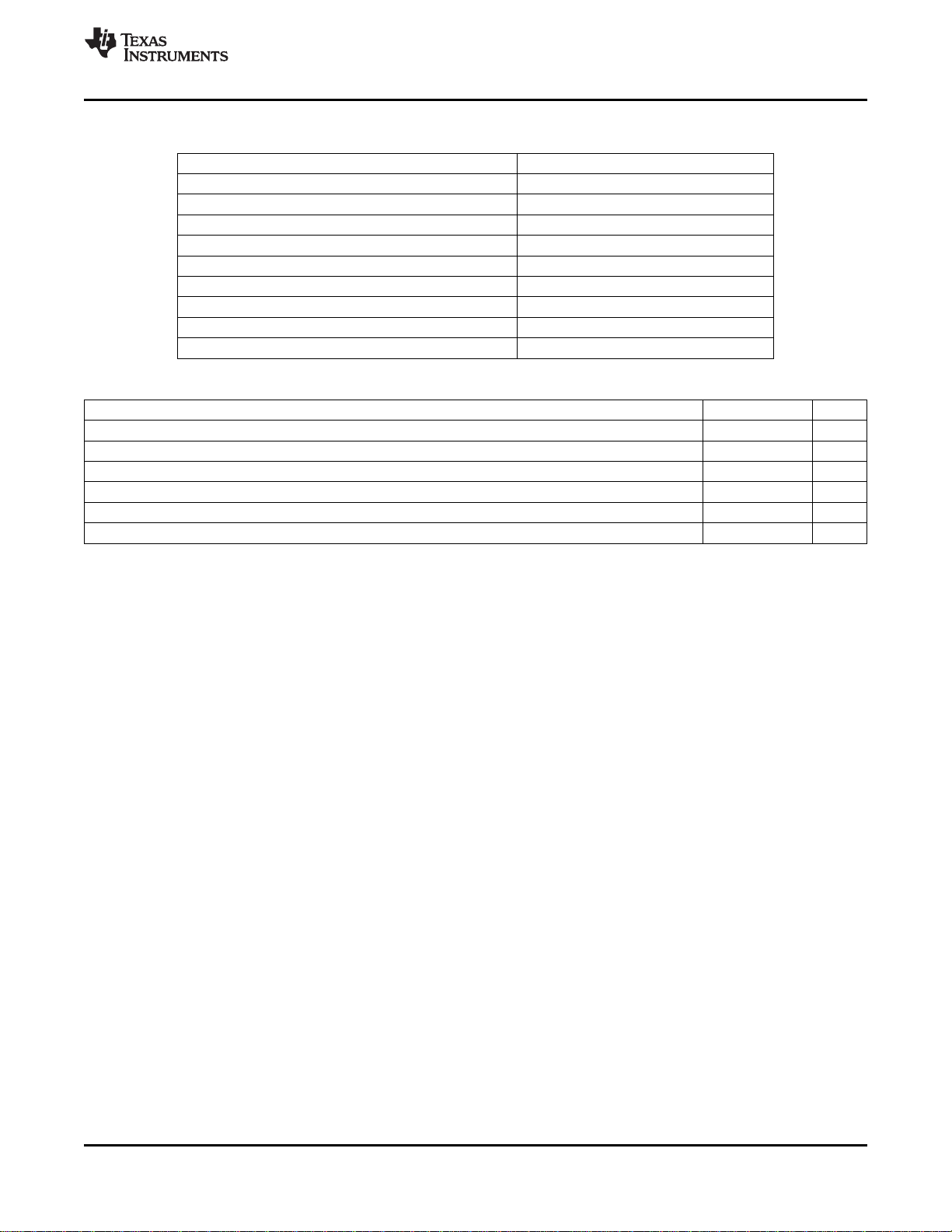
–40°C to 85°C uQFN 0.4-mm pitch – RSV Tape and Reel TSU6111ARSVR ZTN
(1) For the most current package and ordering information, see the Package Option Addendum at the end of this document, or see the TI
Web site at www.ti.com.
(2) Package drawings, thermal data, and symbolization are available at www.ti.com/packaging.
1
PACKAGE
ORDERING INFORMATION
Please be aware that an important notice concerning availability, standard warranty, and use in critical applications of
Texas Instruments semiconductor products and disclaimers thereto appears at the end of this data sheet.
PRODUCTION DATA information is current as of publication date.
Products conform to specifications per the terms of the Texas
Instruments standard warranty. Production processing does not
necessarily include testing of all parameters.
(2)
(1)
ORDERABLE PART NUMBER TOP-SIDE MARKING
Copyright © 2012, Texas Instruments Incorporated
Page 2
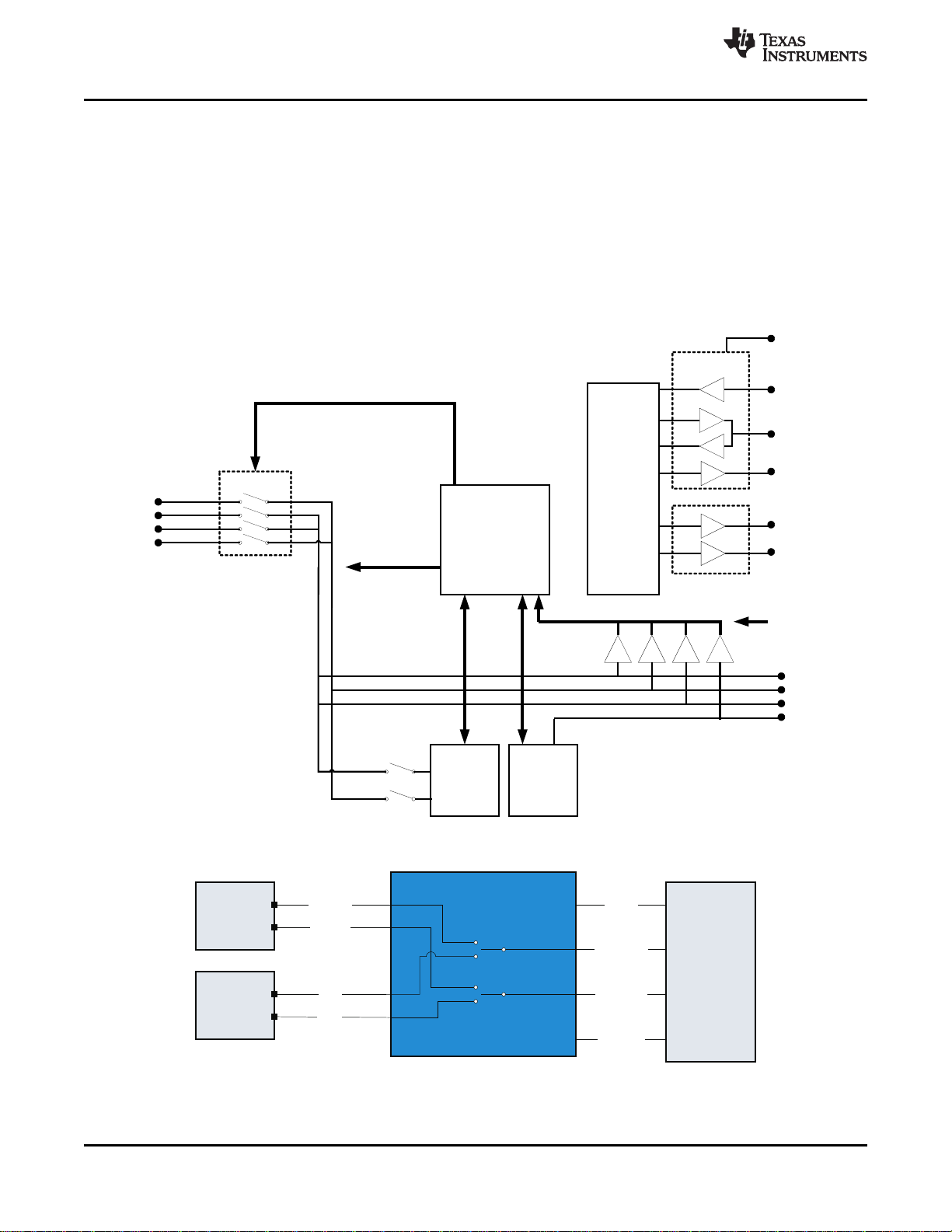
UART
USB
Micro
USB
DP_HT
TxD
RxD
TSU6111 SWITCH
MATRIX
DM_HT VBUS
DM_CON
DP_CON
ID_CON
Charger
Detection
Sources
And
Comp’s
Accessory
ID
Detection
ADC
I2C Interface
&
Hardware
Control
VBUS
DP
DM
ID
Buffers and/or
Comparators
JIG
INTB
SDA
SCL
VDDIO
BOOT
I2C
Interface
Switches
RxD
TxD
USB_DM
USB_DP
State Machine
Switch
Ctrl
TSU6111A
SCDS331A –FEBRUARY 2012–REVISED AUGUST 2012
www.ti.com
DESCRIPTION
The TSU6111A is a high performance differential autonomous SP2T switch with impedance detection. The
switch supports the detection of various accessories that are attached through DP, DM, and ID. The charger
detection satisfies USB charger specification v1.1 and V
external protection. Power for this device is supplied through VBAT of the system or through V
attached to a charger.
The SP2T switch is controlled by the automatic detection logic or through manual configuration of the I2C. JIG
and BOOT pins are used when a USB or UART JIG cable is used to test the device in the development and
manufacturing. TSU6111A has open-drain JIG output (active low).
BLOCK DIAGRAM
has a 28V tolerance to eliminate the need for
BUS_IN
BUS_IN
when
SWITCH MATRIX
2 Submit Documentation Feedback Copyright © 2012, Texas Instruments Incorporated
Product Folder Link(s): TSU6111A
Page 3
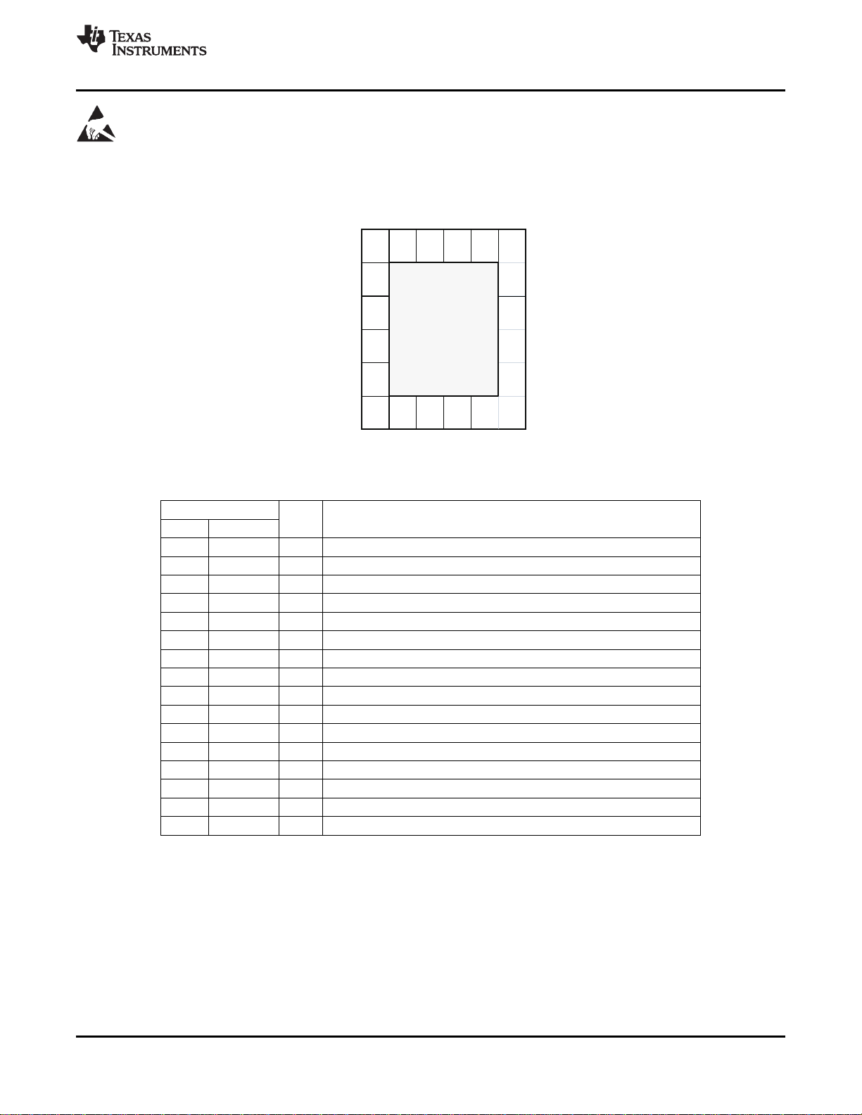
ID_CON
DP_CON
DM_CON
V
BUS_IN
16 15 14 13
DM_HOST 1 12 GND
DP_HOST 2 11 SDA
TxD 3 10 SCL
RxD 4 9 INTB
5 6 7 8
V
BAT
BOOT
JIG
V
DDIO
TSU6111A
www.ti.com
SCDS331A –FEBRUARY 2012–REVISED AUGUST 2012
These devices have limited built-in ESD protection. The leads should be shorted together or the device placed in conductive foam
during storage or handling to prevent electrostatic damage to the MOS gates.
PINOUT DIAGRAM (TOP VIEW)
PIN FUNCTIONS
PIN
NO. NAME
1 DM_HOST I/O USB DM connected to host
2 DP_HOST I/O USB DP connected to host
3 TxD I/O UART Tx
4 RxD I/O UART Rx
5 VBAT I Connected to battery
6 BOOT O BOOT mode out (push-pull). Used for factory test modes.
7 JIG O JIG detection JIG detection (Open-drain). Used for factory test modes
8 VDDIO O I/O voltage reference
9 INTB O Interrupt to host (push-pull)
10 SCL I I2C clock
11 SDA I/O I2C data
12 GND Ground
13 VBUS_IN I VBUS connected to USB receptacle
14 DM_CON I/O USB DM connected to USB receptacle
15 DP_CON I/O USB DP connected to USB receptacle
16 ID_CON I/O USB ID connected to USB receptacle
I/O DESCRIPTION
Copyright © 2012, Texas Instruments Incorporated Submit Documentation Feedback 3
Product Folder Link(s): TSU6111A
Page 4
TSU6111A
SCDS331A –FEBRUARY 2012–REVISED AUGUST 2012
ABSOLUTE MAXIMUM RATINGS
(1)(2)
www.ti.com
over operating free-air temperature range (unless otherwise noted)
MIN MAX UNIT
V
BUS
V
BAT
V
DDIO
V
ID_CON
V
USBIO
V
UARTIO
V
JIG
V
LOGIC_O
I
K
I
SW-DC
I
SW
I
IK
I
LOGIC_O
I
GND
T
stg
(1) Stresses above these ratings may cause permanent damage. Exposure to absolute maximum conditions for extended periods may
degrade device reliability. These are stress ratings only, and functional operation of the device at these or any other conditions beyond
those specified is not implied.
(2) The algebraic convention, whereby the most negative value is a minimum and the most positive value is a maximum.
Supply voltage from USB connector –0.5 28
Supply voltage from battery –0.5 6.0
Logic supply voltage –0.5 4.6 V
ID Connector voltage –0.5 V
Switch I/O voltage range USB Switch –0.5 V
Switch I/O voltage range UART Switch –0.5 V
JIG voltage –0.5 V
+0.5 V
BAT
+0.5 V
BAT
+0.5 V
BAT
+0.5 V
BAT
Voltage applied to logic output (SCL, SDA, INTB, BOOT) –0.5 4.6 V
Analog port diode current –50 50 mA
ON-state continuous switch current –60 60 mA
ON-state peak switch current PEAK –150 150 mA
Digital logic input clamp current V
< 0 –50 mA
DDIO
Continuous current through logic output (SCL, SDA, INTB, BOOT) –50 50 mA
Continuous current through GND 100 mA
Storage temperature range –65 150 °C
V
THERMAL IMPEDANCE RATINGS
θJA Package thermal impedance RSV package 184 °C/W
UNIT
4 Submit Documentation Feedback Copyright © 2012, Texas Instruments Incorporated
Product Folder Link(s): TSU6111A
Page 5
TSU6111A
www.ti.com
SCDS331A –FEBRUARY 2012–REVISED AUGUST 2012
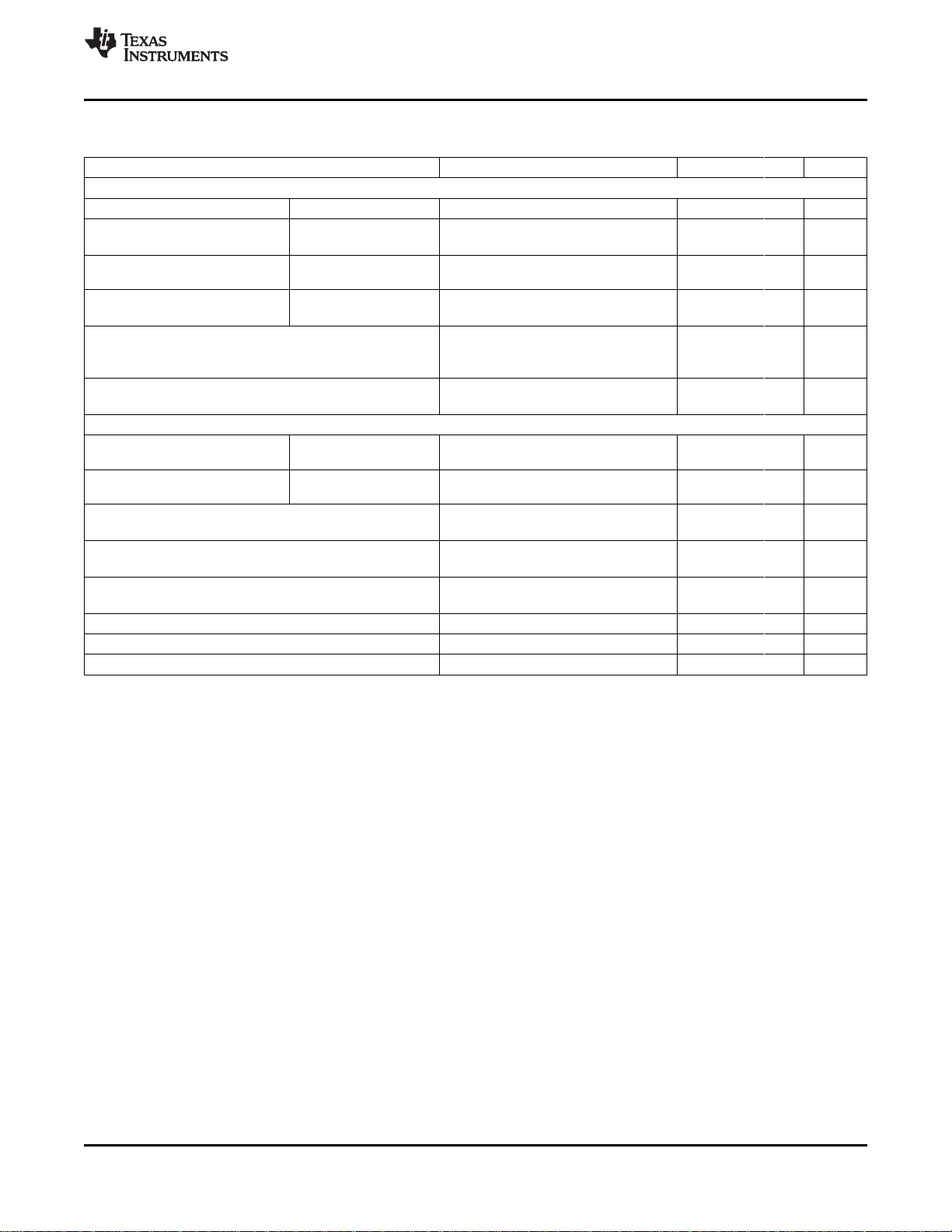
SUMMARY OF TYPICAL CHARACTERISTICS
AMBIENT TEMPERATURE = 25°C USB/UART PATH
Number of channels 2
ON-state resistance (ron) 8 Ω
ON-state resistance match (Δron) 0.5 Ω
ON-state resistance flatness (r
Turn-on/turn-off time (tON/t
OFF
) 0.5 Ω
on(flat)
) 95 µs/ 3.5 µs
Bandwidth (BW) 920 MHz
OFF isolation (O
Crosstalk (X
Leakage current (I
) –26 dB at 250 MHz
ISO
) –32 dB at 250 MHz
TALK
) 50 nA
IO(ON)
RECOMMENDED OPERATING CONDITIONS
MIN MAX UNIT
V
BUS_IN
V
BAT
V
DDIO
ID_CON_Cap ID_CON capacitance 1 nF
USB_I/O USB path signal range 0 3.6 V
Temperature Operating Temperature –40 85 °C
VBUS voltage 4.0 6.5 V
VBAT voltage 3.0 4.4 V
VDDIO voltage 1.65 3.6 V
Copyright © 2012, Texas Instruments Incorporated Submit Documentation Feedback 5
Product Folder Link(s): TSU6111A
Page 6
TSU6111A
SCDS331A –FEBRUARY 2012–REVISED AUGUST 2012
www.ti.com
ELECTRICAL SPECIFICATION
over operating free-air temperature range (unless otherwise noted)
PARAMETERS TEST CONDITIONS MIN MAX UNIT
DIGITAL SIGNALS – I2C INTERFACE (SCL and SDA)
V
DDIO
V
IH
V
IL
V
OH
V
OL
f
SCL
JIG OUTPUT (TSU6111A – OPEN-DRAIN OUTPUT, ACTIVE LOW)
V
OL
INTB AND BOOT (PUSH-PULL OUTPUT)
V
OH
V
OL
ELECTRICAL SPECIFICATIONS
over operating free-air temperature range (unless otherwise noted)
TOTAL SWITCH CURRENT CONSUMPTION
I
BAT(Standby)
I
DD(Operating)
VOLTAGE PROTECTION
V
VBUS_UVLO
V
VBAT_UVLO
V
VDDIO_UVLO
(1) VOis equal to the asserted voltage on DP_CON and DM_CON pins. VIis equal to the asserted voltage on DP_HT and DM_HT pins. I
is equal to the current on the DP_CON and DM_CON pins. IIis equal to the current on the DP_HT and DM_HT pins.
Logic and I/O supply voltage 1.65 3.6 V
High-level input voltage V
Low-level input voltage 0 V
High-level output voltage IOH= –3 mA V
× 0.7 V
DDIO
× 0.3 V
DDIO
× 0.7 V
DDIO
DDIO
V
Low-level output voltage IOL= 3 mA 0.4 V
SCL frequency 400 kHz
Low-level output voltage IOL= 10 mA, V
High-level output voltage IOH= –4 mA , V
Low-level output voltage IOL= 4 mA , V
(1)
= 3.0 V 0.5 V
BAT
= 1.65 V 1.16 V
DDIO
= 1.65 V 0 0.33 V
DDIO
DDIO
V
PARAMETER TEST CONDITIONS MIN TYP MAX UNIT
V
Standby current consumption V
BAT
V
Operating current consumption V
BAT
V
under voltage + Voltage is rising 2.85
BUS
V
under voltage– Voltage is falling 2.55
BUS
V
under voltage + Voltage is rising 2.65
BUS
V
under voltage– Voltage is falling 2.45
BUS
V
under voltage + Voltage is rising 1.30
BUS
V
under voltage– Voltage is falling 1.05
BUS
= 0 V, Idle state 25 30 µA
BUS
= 0 V, USB switches ON 45 75 µA
BUS_IN
V
V
V
O
6 Submit Documentation Feedback Copyright © 2012, Texas Instruments Incorporated
Product Folder Link(s): TSU6111A
Page 7
TSU6111A
www.ti.com
USB AND UART SWITCH ELECTRICAL CHARACTERISTICS
SCDS331A –FEBRUARY 2012–REVISED AUGUST 2012
(1)
over operating free-air temperature range (unless otherwise noted)
PARAMETER TEST CONDITIONS MIN TYP MAX UNIT
ANALOG SWITCH
V
r
ON
Δr
r
ON(flat)
I
IO(OFF)VI
I
IO(ON)VO
DYNAMIC
t
ON
t
OFF
C
C
C
C
BW Bandwidth RL= 50 Ω, Switch ON 920 MHz
O
X
Analog signal range 0 V
USBIO
ON-state resistance 8 15 Ω
ON-state resistance DM_HT, DP_HT,
ON
match between channels DM_CON, DP_CON
ON-state resistance
flatness
DM_HT, DP_HT, VI= 0 V to 3.6 V, IO= –2 mA,
DM_CON, DP_CON V
= 3.0 V
BAT
VI= 0.4 V, IO= –2 mA, V
BAT
DM_HT, DP_HT, VI= 0 V to 3.6 V, IO= –2 mA,
DM_CON, DP_CON V
BAT
= 3.0 V
= 3.0 V 0.5 2 Ω
VI= 0.3 V, VO= 2.7 V or
or VOOFF leakage current VI= 2.7 V, VO= 0.3 V, 45 200 nA
V
= 4.4 V, Switch OFF
BAT
ON leakage current 50 200 nA
Turn-ON time VIor VO= V
Turn-OFF time VIor VO= V
I(OFF)VI
O(OFF)VO
I(ON)
O(ON)
ISO
TALK
OFF capacitance 4 pF
OFF capacitance 7 pF
, DC bias = 0 V or 3.6 V, f = 10 MHz,
VI, VOON capacitance 9 pF
OFF Isolation f = 240 MHz, RL= 50 Ω, Switch OFF –26 dB
Crosstalk f = 240 MHz, RL= 50 Ω –32 dB
From receipt of I2C ACK
bit
From receipt of I2C ACK
bit
VI= OPEN, VO= 0.3 V or 2.7 V,
V
= 4.4 V, Switch ON
BAT
, RL= 50 Ω, CL= 35 pF 95 µs
BAT
, RL= 50 Ω, CL= 35 pF 3.5 µs
BAT
DC bias = 0 V or 3.6 V, f = 10 MHz,
Switch OFF
DC bias = 0 V or 3.6 V, f = 10 MHz,
Switch OFF
Switch ON
BAT
0.5 2 Ω
V
(1) VOis equal to the asserted voltage on DP_CON and DM_CON pins. VIis equal to the asserted voltage on DP_HT and DM_HT pins. I
is equal to the current on the DP_CON and DM_CON pins. IIis equal to the current on the DP_HT and DM_HT pins.
O
Copyright © 2012, Texas Instruments Incorporated Submit Documentation Feedback 7
Product Folder Link(s): TSU6111A
Page 8
TSU6111A
SCDS331A –FEBRUARY 2012–REVISED AUGUST 2012
www.ti.com
GENERAL OPERATION
The TSU6111A will automatically detect accessories plugged into the phone via the mini/micro USB 5 pin
connector. The type of accessory detected will be stored in I2C registers within the TSU6111A for retrieval by the
host. The TSU6111A has a network of switches that are automatically opened and closed based on the
accessory detection. See Table 1 for details of which switches are open during each mode of operation. The
TSU6111A also offers a manual switching mode that allows the host processor to decide which switches should
be opened and closed. The manual switching settings are executed through the I2C interface.
STANDBY MODE
Standby mode is the default mode upon power up and occurs when no accessory has been detected. During this
mode, the VBUS and ID lines are continually monitored through comparators to determine when an accessory is
inserted. Power consumption is minimal during standby mode.
POWER SUPERVISOR
TSU6111A uses VBAT as the primary supply voltage. VBUS is the secondary supply. VDDIO is used for I2C
communication.
Table 1. Function Table
TSU6111A
VBAT VBUS VDDIO DETECTION I2C COMMENTS
Yes No No Enabled Not enabled VBAT is supply
Yes Yes No Enabled Not enabled VBAT is supply
Yes No Yes Enabled Enabled VBAT is supply
Yes Yes Yes Enabled Enabled VBAT is supply
No Yes No Enabled Not enabled VBUS is supply
No Yes Yes Not valid
No No Yes Not valid
No No No Power Down Reset
8 Submit Documentation Feedback Copyright © 2012, Texas Instruments Incorporated
Product Folder Link(s): TSU6111A
Page 9
TSU6111A
www.ti.com
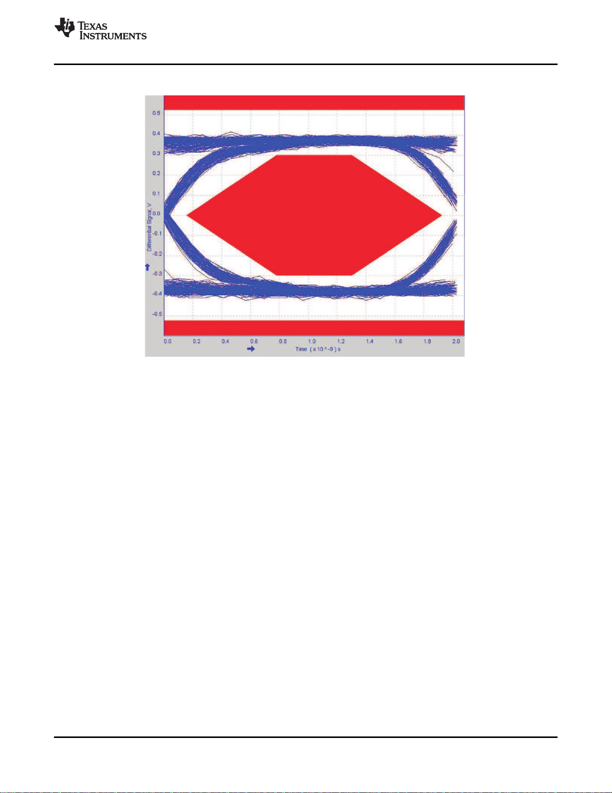
EYE DIAGRAM USB 2.0 HIGH SPEED
SCDS331A –FEBRUARY 2012–REVISED AUGUST 2012
Copyright © 2012, Texas Instruments Incorporated Submit Documentation Feedback 9
Product Folder Link(s): TSU6111A
Page 10
TSU6111A
SCDS331A –FEBRUARY 2012–REVISED AUGUST 2012
www.ti.com
ACCESSORY ID DETECTION
If V
low and an accessory is attached, then use an ADC for impedance sensing on the ID pin to identify which
accessory is attached.
is high and the attachment is not a charger, then determine the impedance on the ID pin. If V
BUS_IN
BUS_IN
IMPEDANCE BUCKETS FOR EACH ACCESSORY
In order to implement ID detection, each accessory should contain a ID impedance resistor value (refer
toTable 2) which has a 5% tolerance accuracy.
Table 2. Accessory ID and Switch States
ACCCESSORY IMPEDANCE TOLERANCE DP/DM
DETECTED RESISTOR
ON ID (%)
OTG 0 — 0 ON OFF OFF OFF
MHL 1K 5% 0 OFF OFF OFF OFF
Audio Device Type 3 28.7K 5% 1110 OFF OFF OFF OFF
Reserved Accessory #1 34K 5% 1111 OFF OFF OFF OFF
Reserved Accessory #2 40.2K 5% 10000 OFF OFF OFF OFF
Reserved Accessory #3 49.9K 5% 10001 OFF OFF OFF OFF
Reserved Accessory #4 64.9K 5% 10010 OFF OFF OFF OFF
Audio Device Type 2 80.27K 5% 10011 OFF OFF OFF OFF
Phone Powered Device 102K 5% 10100 OFF ON OFF OFF
TTY Converter 121K 5% 10101 OFF OFF OFF OFF
UART Cable 150K 5% 10110 OFF ON OFF OFF
Type 1 Charger 200K 5% 10111 OFF OFF OFF OFF
Factory Mode Cable - Boot Off USB 255K 5% 11000 ON OFF ON OFF
Factory Mode Cable - Boot On USB 301K 5% 11001 ON OFF ON ON
Audio/Video Cable 365K 5% 11010 OFF OFF OFF OFF
Type 2 Charger 442K 5% 11011 OFF OFF OFF OFF
Factory Mode Cable - Boot Off UART 523K 5% 11100 OFF ON ON OFF
Factory Mode Cable - Boot On UART 619K 5% 11101 OFF ON ON ON
Stereo Headset with Remote (Audio Device Type 1) 1000.07K 10% 11110 OFF OFF OFF OFF
Mono/Stereo Headset (Audio Device Type 1) 1002K 10% 11110 OFF OFF OFF OFF
No ID — — 11111 OFF OFF OFF OFF
USB Standard Downstream Port — — 11111 ON OFF OFF OFF
USB Charging Downstream Port — — 11111 ON OFF OFF OFF
Dedicated Charging Port — — 11111 OFF OFF OFF OFF
ADC
VALUE
SWITCH STATE FACTORY CABLE
USB UART
JIG BOOT
is
10 Submit Documentation Feedback Copyright © 2012, Texas Instruments Incorporated
Product Folder Link(s): TSU6111A
Page 11
TSU6111A
www.ti.com
SCDS331A –FEBRUARY 2012–REVISED AUGUST 2012
Power-On Reset
When power (from 0 V) is applied to V
until V
has reached V
BAT
. Once V
POR
registers and I2C state machine initialize to their default states.
After the initial power-up phase, V
(V
) for a power-reset cycle.
DDIO
BAT
, an internal power-on reset holds the TSU6111A in a reset condition
BAT
has reached V
BAT
, the reset condition is released, and the TSU6111A
POR
must be lowered to below 0.2 V and then back up to the operating voltage
Software Reset
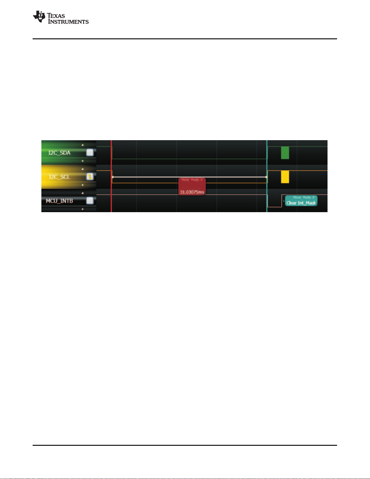
The TSU6111A has software reset feature.
• Hold low both I2C_SCL and I2C_SDA for more than 30ms to reset digital logic of the TSU6111A.
After resetting the digital logic, INTB will keep low until INT_Mask bit of Control register (0x02) is cleared.
Figure 1. Software Reset
Copyright © 2012, Texas Instruments Incorporated Submit Documentation Feedback 11
Product Folder Link(s): TSU6111A
Page 12

SDA
SCL
Data Line Charge
SDA
SCL
S P
Start Condition Stop Condition
TSU6111A
SCDS331A –FEBRUARY 2012–REVISED AUGUST 2012
www.ti.com
Standard I2C Interface Details
The bidirectional I2C bus consists of the serial clock (SCL) and serial data (SDA) lines. The SCL and SDA lines
must be connected to a positive supply via a pull-up resistor when connected to the output stages of a device.
Data transfer may be initiated only when the bus is not busy.
I2C communication with this device is initiated by the master sending a START condition, a high-to-low transition
on the SDA input/output while the SCL input is high (see Figure 2). After the start condition, the device address
byte is sent, MSB first, including the data direction bit (R/W). This device does not respond to the general call
address. After receiving the valid address byte, the device responds with an ACK, a low on the SDA input/output
during the high of the ACK-related clock pulse.
Figure 2. Definition of Start and Stop Conditions
The data byte follows the address ACK. The R/W bit is kept low for transfer from the master to the slave. The
data byte is followed by an ACK sent from this device. Data is sent only if complete bytes are received and
acknowledged. The output data is valid at time (tpv) after the low-to-high transition of SCL, during the clock cycle
for the ACK.
On the I2C bus, only one data bit is transferred during each clock pulse. The data on the SDA line must remain
stable during the high pulse of the clock period, as changes in the data line at this time are interpreted as control
commands (START or STOP, see Figure 3).
Figure 3. Bit Transfer
A Stop condition, a low-to-high transition on the SDA input/output while the SCL input is high, is sent by the
master (see Figure 2).
The number of data bytes transferred between the start and the stop conditions from transmitter to receiver is not
limited. Each byte of eight bits is followed by one ACK bit. The transmitter must release the SDA line before the
receiver can send an ACK bit.
A slave receiver address must generate an ACK after the reception of each byte. The device that acknowledges
has to pull down the SDA line during the ACK clock pulse so that the SDA line is stable low during the high pulse
of the ACK-related clock period (see Figure 4). Setup and hold times must be taken into account.
12 Submit Documentation Feedback Copyright © 2012, Texas Instruments Incorporated
Product Folder Link(s): TSU6111A
Page 13

SDA
ST 0 1 0 0 1 0 1 0 A 1 0 0 0 1 0 0 0 A D7 D6 D5 D4 D3 D2 D1 D0 A D7 D6 D5 D4 D3 D2 D1 D0 A
Start
Slave Address
W/R
Ack. from slave
Sub Address
Ack
from
slave
Auto-Inc.
Ack
from
slave
Data to Timing Set 1
Register
Data to Timing Set 2
Register
Date Byte Date Byte
Register Address
(Timing Set 1 Reg)
SCL
ST
SDA
0 1 0 0 1 0 1 0 A 0 0 0 0 0 0 1 0 A D7 D6 D5 D4 D3 D2 D1 D0 A D7 D6 D5 D4 D3 D2 D1 D0 A SP
Start
Slave Address
W/R
Ack. from slave
Sub Address
Ack
from
slave
Auto-Inc.
Register Address
(Control Reg)
Ack
from
slave
Ack
from
slave
StopData to Control
Register
Data to Control Register
Date Byte Date Byte
Data Output
by Transmitter
Data Output
by Receiver
SCL From
Master
Start
Condition
Clock Pulse for
Acknowledgment
ACK
NACK
1 2 8 9
TSU6111A
www.ti.com
SCDS331A –FEBRUARY 2012–REVISED AUGUST 2012
Figure 4. Acknowledgment on I2C Bus
Writes
Data is transmitted to the TSU6111A by sending the device slave address and setting the LSB to a logic 0 (see
Figure 5 for device address). The command byte is sent after the address and determines which register
receives the data that follows the command byte. The next byte is written to the specified register on the rising
edge of the ACK clock pulse.
Figure 5. Repeated Data Write to a Single Register
Figure 6. Burst Data Write to Multiple Registers
Reads
The bus master must first send the TSU6111A slave address with the LSB set to logic 0. The command byte is
sent after the address and determines which register is accessed. After a restart, the device slave address is
sent again but, this time, the LSB is set to logic 1. Data from the register defined by the command byte then is
sent by the TSU6111A. Data is clocked into the SDA output shift register on the rising edge of the ACK clock
pulse (See Figure 7).
Copyright © 2012, Texas Instruments Incorporated Submit Documentation Feedback 13
Product Folder Link(s): TSU6111A
Page 14

SDA
ST 0 1 0 0 1 0 1 0 A 0 0 0 0 0 0 1 1 A SP 0 1 0 0 1 0 1 1 A D7 D6 D5 D4 D3 D2 D1 D0
Start
Slave Address
W/R
Ack. from slave
Sub Address
Ack
from
slave
Auto-Inc.
Slave Address
W/R
Ack. from slaveStop
Date Byte
A A
Ack. from master
D7 D6 D5 D4 D3 D2 D1 D0
Date Byte
NAD7 D6 D5 D4 D3 D2 D1 D0
Date Byte
Data from Interrupt 1 Reg.
Ack. from master No Ack. from master (Message ends)
Continued
SP
Stop
ST
StartRegister Address
(Interrupt 1 Reg)
Data from Interrupt 1 Reg.Data from Interrupt 1 Reg.
SCL
SDA
ST 0 1 0 0 1 0 1 0 A 1 0 0 0 0 0 1 1 A RS 0 1 0 0 1 0 1 1 A D7 D6 D5 D4 D3 D2 D1 D0
Start
Slave Address
W/R
Ack. from slave
Sub Address
Ack
from
slave
Auto-Inc.
Slave Address
W/R
Ack. from slave
Re-Start
Date Byte
A A
Ack. from master
D7 D6 D5 D4 D3 D2 D1 D0
Date Byte
NA
D7 D6 D5 D4 D3 D2 D1 D0
Date Byte
Data from Interrupt 1 Reg.
Data from Interrupt 2 Reg. Data from Int Mask 1 Reg.
Ack. from master No Ack. from master (Message ends)
Continued
SP
Stop
Register Address
(Interrupt 1 Reg)
SDA
ST 0 1 0 0 1 0 1 0 A 0 0 0 0 0 0 1 1 A RS 0 1 0 0 1 0 1 1 A D7 D6 D5 D4 D3 D2 D1 D0
Start
Slave Address
W/R
Ack. from slave
Sub Address
Ack
from
slave
Auto-Inc.
Slave Address
W/R
Ack. from slave
Re-Start
Date Byte
A A
Ack. from master
D7 D6 D5 D4 D3 D2 D1 D0
Date Byte
NAD7 D6 D5 D4 D3 D2 D1 D0
Date Byte
Data from Interrupt 1 Reg.
Data from Interrupt 1 Reg. Data from Interrupt 1 Reg.
Ack. from master
No Ack. from master (message ends)
Continued
SP
Stop
Register Address
(Interrupt 1 Reg)
TSU6111A
SCDS331A –FEBRUARY 2012–REVISED AUGUST 2012
Figure 7. Repeated Data Read from a Single Register – Combined Mode
www.ti.com
Figure 8. Burst Data Read from Multiple Registers – Combined Mode
Figure 9. Repeated Data Read from a Single Register – Split Mode
14 Submit Documentation Feedback Copyright © 2012, Texas Instruments Incorporated
Product Folder Link(s): TSU6111A
Page 15

SCL
SDA ST 0 1 0 0 1 0 1 0 A 1 0 0 0 0 0 1 1 A SP 0 1 0 0 1 0 1 1 A D7 D6 D5 D4 D3 D2 D1 D0
Start
Slave Address
W/R
Ack. from slave
Sub Address
Ack
from
slave
Auto-Inc.
Slave Address
W/R
Ack. from slaveStop
Date Byte
A A
Ack. from master
D7 D6 D5 D4 D3 D2 D1 D0
Date Byte
NAD7 D6 D5 D4 D3 D2 D1 D0
Date Byte
Data from Interrupt 1 Reg.
Data from Interrupt 2 Reg. Data from Int Mask 1 Reg.
Ack. from master No Ack. from master (Message ends)
Continued
SP
Stop
ST
StartRegister Address
(Interrupt 1 Reg)
TSU6111A
www.ti.com
SCDS331A –FEBRUARY 2012–REVISED AUGUST 2012
Figure 10. Burst Data Read from Multiple Registers – Split Mode
Notes (Applicable to Figure 5–Figure 10):
• SDA is pulled low on Ack. from slave or Ack. from master.
• Register writes always require sub-address write before first data byte.
• Repeated data that writes to a single register continues indefinitely until a Stop or a Re-Start.
• Repeated data reads from a single register continues indefinitely until No Ack. from master.
• Burst data writes start at the specified register address, then advance to the next register address, even to
the read-only registers. For these registers, data write appears to occur; however, no data is changed by the
writes. After register 14h is written, writing resumes to register 01h and continues until a Stop or a Re-Start.
• Burst data reads starts at the specified register address, then advances to the next register address. Once
register 14h is read, reading resumes from register 01h and continues until No Ack. from master.
Copyright © 2012, Texas Instruments Incorporated Submit Documentation Feedback 15
Product Folder Link(s): TSU6111A
Page 16

TSU6111A
SCDS331A –FEBRUARY 2012–REVISED AUGUST 2012
I2C Register Map
ADDR REGISTER TYPE BIT7 BIT6 BIT5 BIT4 BIT3 BIT2 BIT1 BIT0
01h Device ID R 00010010 Version ID Vendor ID
02h Control R/W xxx11111 Switch Open Raw Data Manual S/W Wait INT Mask
03h Interrupt 1 R xxxxxx00 Detach Attach
04h Interrupt 2 R xx0xx000 CONNECT ADC_Change Charging_A/V
05h Interrupt Mask 1 R/W xxxxxx00 Detach Attach
06h Interrupt Mask 2 R/W xx0xx000 CONNECT ADC_Change Charging_A/V
07h ADC R xxx11111 ADC Value
08h Timing Set 1 R/W xxxx0000 Device Wake Up
09h Timing Set 2 R/W 0000xxxx Switching Wait
0Ah Device Type 1 R 00000000 USG OTG DCP CDP UART USG Audio Type2 Audio Type1
0Bh Device Type 2 R 00000000 Audio/Video TTY PPD JIG_USB_OFF JIG_USB_ON
0Ch Button 1 R 00000000 7 6 5 4 3 2 1 Send_End
0Dh Button 2 R x0000000 Unknown Error 12 11 10 9 8
13h Manual S/W 1 R/W 000000xx D– Switching D+ Switching
14h Manual S/W 2 R/W xxxx00xx BOOT_SW JIG-ON
15h Device Type 3 R xxxxxx00 VBUS MHL
(1)(2)(3)
RESET
VALUE
Audio
Type3
Reserved_
Attach
Reserved_
Attach
JIG_UART_ JIG_UART_
OFF ON
www.ti.com
(1) Do not use blank register bits.
(2) Write “0” to the blank register bits.
(3) Values read from the blank register bits are not defined and invalid.
16 Submit Documentation Feedback Copyright © 2012, Texas Instruments Incorporated
Product Folder Link(s): TSU6111A
Page 17

TSU6111A
www.ti.com
SCDS331A –FEBRUARY 2012–REVISED AUGUST 2012
Slave Address
NAME
Slave address 8 0 1 0 0 1 0 1 R/W
SIZE
(BITS)
BIT 7 BIT 6 BIT 5 BIT 4 BIT 3 BIT 2 BIT 1 BIT 0
DESCRIPTION
Device ID
Address: 01h
Reset Value: 00010010
Type: Read
BIT NO. NAME SIZE (BITS) DESCRIPTION
2-0 Vendor ID 3 A unique number for vendor 010 for Texas Instruments
7-3 Version ID 5 A unique number for chip version 00001b for TSU6111A
Control
Address: 02h
Reset Value: xxx11111
Type: Read/Write
BIT NO. NAME SIZE (BITS) DESCRIPTION
0 INT Mask 1 0: Unmask interrupt
1: Mask interrupt
1 Wait 1 0: Wait until host re-sets this bit(WAIT bit) high
1: Wait until Switching timer is expired
2 Manual S/W 1 0: Manual Switching
1: Automatic Switching
3 RAW Data 1 0: Report the status changes on ID to Host
1: Don't report the status changes on ID
4 Switch Open 1 0: Open all Switches
1: Automatic Switching by accessory status
7-5 Reserved
Copyright © 2012, Texas Instruments Incorporated Submit Documentation Feedback 17
Product Folder Link(s): TSU6111A
Page 18

TSU6111A
SCDS331A –FEBRUARY 2012–REVISED AUGUST 2012
Interrupt 1
Address: 03h
Reset Value: xxxxxx00
Type: Read and Clear
BIT NO. NAME SIZE (BITS) DESCRIPTION
0 Attach 1 1: Accessory is attached
1 Detach 1 1: Accessory is detached
7-2 Unused 6 Unused
Interrupt 2
Address: 04h
Reset Value:xx0xx000
Type: Read and Clear
BIT NO. NAME SIZE (BITS) DESCRIPTION
0 Charging_A/V 1 1: Charger detected when A/V cable is attached
1 Reserved_Attach 1 1: Reserved Device is attached
2 ADC_Change 1 1: ADC value is changed when RAW data is enabled
4-3 Unused 2
5 Connect 1 1: Switch is connected(closed)
7-6 Unused 2
www.ti.com
18 Submit Documentation Feedback Copyright © 2012, Texas Instruments Incorporated
Product Folder Link(s): TSU6111A
Page 19

TSU6111A
www.ti.com
Interrupt Mask 1
Address: 05h
Reset Value:xxxxxx00
Type: Read/Write
BIT NO. NAME SIZE (BITS) DESCRIPTION
0 Attach 1 0: Unmask Attach Interrupt
1: Mask Attach Interrupt
1 Detach 1 0: Unmask Key press Interrupt
1: Mask Detach Interrupt
7-2 Unused 6 Unused
Interrupt Mask 2
Address: 06h
Reset Value:xx0xx000
Type: Read/Write
BIT NO. NAME SIZE (BITS) DESCRIPTION
0 Charging_A/V 1 0: Unmask A/V_Charging Interrupt
1: Mask A/V_Charging Interrupt
1 Reserved_Attach 1 0: Unmask Reserved_Attach Interrupt
1: Mask Reserved_Attach Interrupt
2 ADC_Change 1 0: Unmask ADC_Change Interrupt
1: Mask ADC_Change Interrrupt
4-3 Unused 2
5 Connect 1 0: Unmask Connect Interrupt
1: Mask Connect Interrupt
7-6 Unused 2
SCDS331A –FEBRUARY 2012–REVISED AUGUST 2012
Copyright © 2012, Texas Instruments Incorporated Submit Documentation Feedback 19
Product Folder Link(s): TSU6111A
Page 20

TSU6111A
SCDS331A –FEBRUARY 2012–REVISED AUGUST 2012
ADC Value
Address: 07h
Reset Value: xxx11111
Type: Read
BIT NO. NAME SIZE (BITS) DESCRIPTION
4-0 ADC value 5 ADC value read from ID
7-5 Unused 3
Timing Set 1
Address: 08h
Reset Value: xxxx0000
Type: Read/Write
BIT NO. NAME SIZE (BITS) DESCRIPTION
3-0 Device Wake Up 4 Device wake up duration
7-4 Unused 4
Timing Set 2
Address: 09h
Reset Value: 0000xxxx
Type: Read/Write
BIT NO. NAME SIZE (BITS) DESCRIPTION
3-0 Unused 4
7-4 Switching wait 4 Waiting duration before switching
www.ti.com
Time Table
SETTING VALUE DEVICE WAKE UP SWITCHING WAIT
0000 50 ms 10 ms
0001 100 ms 30 ms
0010 150 ms 50 ms
0011 200 ms 70 ms
0100 300 ms 90 ms
0101 400 ms 110 ms
0110 500 ms 130 ms
0111 600 ms 150 ms
1000 700 ms 170 ms
1001 800 ms 190 ms
1010 900 ms 210 ms
1011 1000 ms –
1100 – –
1101 – –
1110 – –
1111 – –
(1) Maximum variation of these timing is ±20%
(1)
20 Submit Documentation Feedback Copyright © 2012, Texas Instruments Incorporated
Product Folder Link(s): TSU6111A
Page 21

TSU6111A
www.ti.com
SCDS331A –FEBRUARY 2012–REVISED AUGUST 2012
Device Type 1
Address: 0Ah
Reset Value: 00000000
Type: Read
BIT NO. NAME SIZE (BITS) DESCRIPTION
0 Audio type 1 1 Audio device type 1
1 Audio type 2 1 Audio device type 2
2 USB 1 USB host
3 UART 1 UART
4 Unused 1 Unused
5 CDP 1 Charging Downstream Port (USB Host Hub Charger)
6 DCP 1 Dedicated Charging Port
7 USB OTG 1 USB on-the-go device
Device Type 2
Address: 0Bh
Reset Value:00000000
Type: Read
BIT NO. NAME SIZE (BITS) DESCRIPTION
0 JIG_USB_ON 1 Factory mode cable
1 JIG_USB_OFF 1 Factory mode cable
2 JIG_UART_ON 1 Factory mode cable
3 JIG_UART_OFF 1 Factory mode cable
4 PPD 1 Phone-powered device
5 TTY 1 TTY converter
6 Audio/Video 1 A/V cable
7 Audio type 3 1 Audio device type 3
Copyright © 2012, Texas Instruments Incorporated Submit Documentation Feedback 21
Product Folder Link(s): TSU6111A
Page 22

TSU6111A
SCDS331A –FEBRUARY 2012–REVISED AUGUST 2012
Button 1
Address: 0Ch
Reset Value: 00000000
Type: Read and Clear
BIT NO. NAME SIZE (BITS) DESCRIPTION
0 Send_End 1 Send_End key is pressed
1 1 1 Number 1 key is pressed
2 2 1 Number 2 key is pressed
3 3 1 Number 3 key is pressed
4 4 1 Number 4 key is pressed
5 5 1 Number 5 key is pressed
6 6 1 Number 6 key is pressed
7 7 1 Number 7 key is pressed
Button 2
Address: 0Dh
Reset Value:x0000000
Type: Read and Clear
BIT NO. NAME SIZE (BITS) DESCRIPTION
0 8 1 Number 8 key is pressed
1 9 1 Number 9 key is pressed
2 10 1 Number 10 key is pressed
3 11 1 Number 11 key is pressed
4 12 1 Number 12 key is pressed
5 Error 1 Error key is pressed
6 Unknown 1 Unknown key is pressed
7 Unused
www.ti.com
22 Submit Documentation Feedback Copyright © 2012, Texas Instruments Incorporated
Product Folder Link(s): TSU6111A
Page 23

TSU6111A
www.ti.com
Manual S/W 1
Address: 13h
Reset Value: 000000xx
Type: Read/Write
BIT NO. NAME SIZE (BITS) DESCRIPTION
1-0 Unused 2
4-2 D+ Switching 3 000: Open all switch
001: D+ is connected to D+ of USB port
010: Open all switch
011: D+ is connected to RxD of UART
7-5 D– Switching 3 000: Open all switch
001: D– is connected to D– of USB port
010: Open all switch
011: D– is connected to TxD of UART
Manual S/W 2
Address: 14h
Reset Value: xxxx00xx
Type: Read/Write
BIT NO. NAME SIZE (BITS) DESCRIPTION
1-0 Unused 2
2 JIG 1 TSU6111A:
0: High Impedance
1: GND
3 BOOT 1 0: Low
1: High
7-4 Unused 4
SCDS331A –FEBRUARY 2012–REVISED AUGUST 2012
Device Type 3
Address: 15h
Reset Value: xxxxxx00
Type: Read
BIT NO. NAME SIZE (BITS) DESCRIPTION
0 MHL 2 MHL device
1 VBUS 1 VBUS valid
7-1 Unused 7 Unused
Copyright © 2012, Texas Instruments Incorporated Submit Documentation Feedback 23
Product Folder Link(s): TSU6111A
Page 24

MICRO
USB
V+
DN
DP
ID
GND
TSU6111A
INTB
DP_HOST
DM_HOST
RxD
TxD
VBUS
DM_CON
DP_CON
ID_CON
GND
AP OR
BASEBAND
1pF ~
10pF
ESD
2.2 Ω
1p F
ESD
2.2 Ω
1p F
ESD
2.2 Ω
1p F
ESD
1µF ~
10µF
1.7 ~ 3.6V
SCL
SDA
JIG
INTB
DP_HOST
DM_HOST
RxD
TxD
SCL
SDA
JIG
1k Ω ~
10kΩ
VDDIO
VDDIO
VBAT
1µF~
10µF
1µF~
10µF
Battery
BOOT
BOOT
VBAT
1k Ω ~
10k Ω
1k Ω ~
10k Ω
0.1µF
0.1µF
0.1µF
TSU6111A
SCDS331A –FEBRUARY 2012–REVISED AUGUST 2012
APPLICATION SCHEMATIC
PIN NAME PIN NO. CRITICAL COMPONENT
V
BUS_IN
V
DDIO
V
BAT
Jig 7 1kΩ
SCL 10 1kΩ
SDA 11 1kΩ
DM_CON 14
DP_CON 15
ID_CON 16
(1) Optional components
1µF~10µF
13 ESD Protection Diode
0.1µF
1µF~10µF
8
0.1µF
1µF~10µF
5 Battery
0.1µF
2.2Ω
ESD Protection Diode
2.2Ω
ESD Protection Diode
(1)
2.2Ω
ESD Protection Diode
www.ti.com
24 Submit Documentation Feedback Copyright © 2012, Texas Instruments Incorporated
Product Folder Link(s): TSU6111A
Page 25

TSU6111A
www.ti.com
SCDS331A –FEBRUARY 2012–REVISED AUGUST 2012
SCHEMATIC GUIDELINES
1. V
elements. The capacitors act as a shunt to block off the noise. The 0.1µF capacitor smoothes out high
frequencies and has a lower series inductance. The 1µF~10µF capacitors smoothes out the lower
frequencies and has a much higher series inductance. Placing both capacitors will provide better load
regulation across the frequency spectrum.
2. JIG is an open-drain output and therefore requires a 1kΩ ~ 10kΩ pull-up resistor to VBAT.
3. SCL and SDA require 1kΩ ~ 10kΩ pull-up resistors to VDDIO to prevent floating inputs.
4. V
ballasting to protect the chip and internal circuitry.
(a) For ID_CON, if there is less stress on the ID pin then the external 2.2Ω resistor is optional.
5. DM_CON, DP_CON, and ID_CON are recommended to have a 1pF external ESD Protection Diode rated for
8kV IEC protection to prevent failure in case of an 8kV IEC contact discharge.
6. VBUS_IN is recommended to have a 1pF ~ 10pF external ESD Protection Diode rated for 8kV IEC protection
to prevent failure in case of an 8kV IEC contact discharge.
, V
BUS_IN
, DM_CON, and DP_CON are recommended to have an external resistor 2.2Ω to provide extra
BUS_IN
DDIO
, and V
require 1µF~10µF and 0.1µF decoupling capacitors to reduce noise from circuit
BAT
RECOMMENDED OPERATING CONDITIONS
PARAMETER DESCRIPTION MIN MAX UNIT
V
BUS_IN
V
BAT
V
DDIO
ID_CON_Cap ID_CON capacitance 1 nF
USB_I/O USB path signal range 0 3.6 V
Temperature Operating Temperature –40 85 °C
VBUS voltage 4.0 6.5 V
VBAT voltage 3.0 4.4 V
VDDIO voltage 1.65 3.6 V
Copyright © 2012, Texas Instruments Incorporated Submit Documentation Feedback 25
Product Folder Link(s): TSU6111A
Page 26

DECOUPLING
CAPACITORS
MICRO USB
CONNECTOR
Place the USB connector as close as
possible to the DUT
DUT PAD
45 Degree Turns
on USB signals
USB DP & DM lines
length matched
TSU6111A
SCDS331A –FEBRUARY 2012–REVISED AUGUST 2012
PCB ROUTING GUIDELINES
Routing Guidelines for USB Signal Integrity
1. All the USB lines DP_CON, DM_CON, DP_HT, DM_HT, TxD, and RxD
– Must have 45Ω single ended characteristic impedance
– Must have 90Ω differential ended impedance
– To fulfill USB 2.0 requirements
2. TSU6111A location
– Close to the USB connector as possible
– Keep the distance between the USB controller and the device less than 1 inch
– Shortening the length of the trace will reduce effect of stray noise and radiate less EMI
3. Minimize use of VIAs for USB related signals
– Differential transmission lines should be matched as close as possible
– For optimum USB2.0 performance, use no VIAs
www.ti.com
26 Submit Documentation Feedback Copyright © 2012, Texas Instruments Incorporated
Product Folder Link(s): TSU6111A
Page 27

TSU6111A
www.ti.com
SCDS331A –FEBRUARY 2012–REVISED AUGUST 2012
REVISION HISTORY
Changes from Original (February 2012) to Revision A Page
• Updated ORDERABLE PART NUMBER and TOP-SIDE MARKING in the ORDERING INFORMATION table. ................ 1
Copyright © 2012, Texas Instruments Incorporated Submit Documentation Feedback 27
Product Folder Link(s): TSU6111A
Page 28

PACKAGE OPTION ADDENDUM
www.ti.com
10-Dec-2020
PACKAGING INFORMATION
Orderable Device Status
TSU6111ARSVR ACTIVE UQFN RSV 16 3000 RoHS & Green NIPDAU Level-1-260C-UNLIM -40 to 85 ZTN
(1)
The marketing status values are defined as follows:
ACTIVE: Product device recommended for new designs.
LIFEBUY: TI has announced that the device will be discontinued, and a lifetime-buy period is in effect.
NRND: Not recommended for new designs. Device is in production to support existing customers, but TI does not recommend using this part in a new design.
PREVIEW: Device has been announced but is not in production. Samples may or may not be available.
OBSOLETE: TI has discontinued the production of the device.
Package Type Package
(1)
Drawing
Pins Package
Qty
Eco Plan
(2)
Lead finish/
Ball material
(6)
MSL Peak Temp
(3)
Op Temp (°C) Device Marking
(4/5)
(2)
RoHS: TI defines "RoHS" to mean semiconductor products that are compliant with the current EU RoHS requirements for all 10 RoHS substances, including the requirement that RoHS substance
do not exceed 0.1% by weight in homogeneous materials. Where designed to be soldered at high temperatures, "RoHS" products are suitable for use in specified lead-free processes. TI may
reference these types of products as "Pb-Free".
RoHS Exempt: TI defines "RoHS Exempt" to mean products that contain lead but are compliant with EU RoHS pursuant to a specific EU RoHS exemption.
Green: TI defines "Green" to mean the content of Chlorine (Cl) and Bromine (Br) based flame retardants meet JS709B low halogen requirements of <=1000ppm threshold. Antimony trioxide based
flame retardants must also meet the <=1000ppm threshold requirement.
(3)
MSL, Peak Temp. - The Moisture Sensitivity Level rating according to the JEDEC industry standard classifications, and peak solder temperature.
(4)
There may be additional marking, which relates to the logo, the lot trace code information, or the environmental category on the device.
(5)
Multiple Device Markings will be inside parentheses. Only one Device Marking contained in parentheses and separated by a "~" will appear on a device. If a line is indented then it is a continuation
of the previous line and the two combined represent the entire Device Marking for that device.
(6)
Lead finish/Ball material - Orderable Devices may have multiple material finish options. Finish options are separated by a vertical ruled line. Lead finish/Ball material values may wrap to two
lines if the finish value exceeds the maximum column width.
Important Information and Disclaimer:The information provided on this page represents TI's knowledge and belief as of the date that it is provided. TI bases its knowledge and belief on information
provided by third parties, and makes no representation or warranty as to the accuracy of such information. Efforts are underway to better integrate information from third parties. TI has taken and
continues to take reasonable steps to provide representative and accurate information but may not have conducted destructive testing or chemical analysis on incoming materials and chemicals.
TI and TI suppliers consider certain information to be proprietary, and thus CAS numbers and other limited information may not be available for release.
In no event shall TI's liability arising out of such information exceed the total purchase price of the TI part(s) at issue in this document sold by TI to Customer on an annual basis.
Samples
Addendum-Page 1
Page 29

PACKAGE MATERIALS INFORMATION
www.ti.com 3-Aug-2017
TAPE AND REEL INFORMATION
*All dimensions are nominal
Device Package
Type
TSU6111ARSVR UQFN RSV 16 3000 177.8 12.4 2.0 2.8 0.7 4.0 12.0 Q1
Package
Drawing
Pins SPQ Reel
Diameter
(mm)
Reel
Width
W1 (mm)
A0
(mm)B0(mm)K0(mm)P1(mm)W(mm)
Pin1
Quadrant
Pack Materials-Page 1
Page 30

PACKAGE MATERIALS INFORMATION
www.ti.com 3-Aug-2017
*All dimensions are nominal
Device Package Type Package Drawing Pins SPQ Length (mm) Width (mm) Height (mm)
TSU6111ARSVR UQFN RSV 16 3000 202.0 201.0 28.0
Pack Materials-Page 2
Page 31

PACKAGE OUTLINE
PIN 1 INDEX AREA
0.55
0.45
0.05
0.00
SCALE 5.000
UQFN - 0.55 mm max heightRSV0016A
ULTRA THIN QUAD FLATPACK - NO LEAD
B
1.85
1.75
A
2.65
2.55
C
SEATING PLANE
0.05 C
2X 1.2
SYMM
5
4
12X 0.4
0.55
0.45
SYMM
℄
1
16
2X 1.2
NOTES:
1. All linear dimensions are in millimeters. Any dimensions in parenthesis are for reference only. Dimensioning and tolerancing
per ASME Y14.5M.
2. This drawing is subject to change without notice.
℄
8
13
PIN 1 ID
(45° X 0.1)
15X
9
12
0.45
0.35
0.25
16X
0.15
0.07 C A B
0.05
4220314/C 02/2020
(0.13) TYP
www.ti.com
Page 32

(0.7)
16
SYMM
℄
EXAMPLE BOARD LAYOUT
UQFN - 0.55 mm max heightRSV0016A
ULTRA THIN QUAD FLATPACK - NO LEAD
13
SEE SOLDER MASK
DETAIL
16X (0.2)
(R0.05) TYP
0.05 MAX
ALL AROUND
12X (0.4)
1
4
15X (0.6)
5
(1.6)
8
LAND PATTERN EXAMPLE
EXPOSED METAL SHOWN
SCALE: 25X
ALL AROUND
METAL EDGE
12
SYMM
℄
9
0.05 MIN
(2.4)
METAL UNDER
SOLDER MASK
EXPOSED METAL
NON SOLDER MASK
DEFINED
(PREFERRED)
SOLDER MASK
OPENING
EXPOSED
METAL
SOLDER MASK DEFINED
SOLDER MASK DETAILS
NOTES: (continued)
3. For more information, see Texas Instruments literature number SLUA271 (www.ti.com/lit/slua271).
www.ti.com
SOLDER MASK
OPENING
4220314/C 02/2020
Page 33

(0.7)
16
EXAMPLE STENCIL DESIGN
UQFN - 0.55 mm max heightRSV0016A
ULTRA THIN QUAD FLATPACK - NO LEAD
13
16X (0.2)
12X (0.4)
(R0.05) TYP
1
4
15X (0.6)
5
SYMM
℄
(1.6)
SOLDER PASTE EXAMPLE
BASED ON 0.125 MM THICK STENCIL
SCALE: 25X
12
SYMM
9
8
(2.4)
℄
4220314/C 02/2020
NOTES: (continued)
4. Laser cutting apertures with trapezoidal walls and rounded corners may offer better paste release. IPC-7525 may have alternate
design recommendations.
www.ti.com
Page 34

IMPORTANT NOTICE AND DISCLAIMER
TI PROVIDES TECHNICAL AND RELIABILITY DATA (INCLUDING DATASHEETS), DESIGN RESOURCES (INCLUDING REFERENCE
DESIGNS), APPLICATION OR OTHER DESIGN ADVICE, WEB TOOLS, SAFETY INFORMATION, AND OTHER RESOURCES “AS IS”
AND WITH ALL FAULTS, AND DISCLAIMS ALL WARRANTIES, EXPRESS AND IMPLIED, INCLUDING WITHOUT LIMITATION ANY
IMPLIED WARRANTIES OF MERCHANTABILITY, FITNESS FOR A PARTICULAR PURPOSE OR NON-INFRINGEMENT OF THIRD
PARTY INTELLECTUAL PROPERTY RIGHTS.
These resources are intended for skilled developers designing with TI products. You are solely responsible for (1) selecting the appropriate
TI products for your application, (2) designing, validating and testing your application, and (3) ensuring your application meets applicable
standards, and any other safety, security, or other requirements. These resources are subject to change without notice. TI grants you
permission to use these resources only for development of an application that uses the TI products described in the resource. Other
reproduction and display of these resources is prohibited. No license is granted to any other TI intellectual property right or to any third
party intellectual property right. TI disclaims responsibility for, and you will fully indemnify TI and its representatives against, any claims,
damages, costs, losses, and liabilities arising out of your use of these resources.
TI’s products are provided subject to TI’s Terms of Sale (www.ti.com/legal/termsofsale.html) or other applicable terms available either on
ti.com or provided in conjunction with such TI products. TI’s provision of these resources does not expand or otherwise alter TI’s applicable
warranties or warranty disclaimers for TI products.
Mailing Address: Texas Instruments, Post Office Box 655303, Dallas, Texas 75265
Copyright © 2020, Texas Instruments Incorporated
 Loading...