

Page 1
TSOP28..
Vishay Telefunken
1 (7)Rev. 7, 31-Jan-00
www.vishay.de • FaxBack +1-408-970-5600
Document Number 82058
Photo Modules for PCM Remote Control Systems
Available types for different carrier frequencies
Type fo Type fo
TSOP2830 30 kHz TSOP2833 33 kHz
TSOP2836 36 kHz TSOP2837 36.7 kHz
TSOP2838 38 kHz TSOP2840 40 kHz
TSOP2856 56 kHz
Description
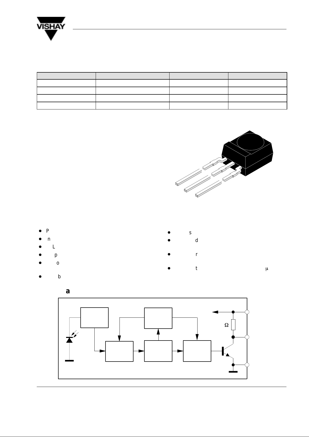
The TSOP28.. – series are miniaturized receivers for
infrared remote control systems. PIN diode and preamplifier are assembled on lead frame, the epoxy
package is designed as IR filter.
The demodulated output signal can directly be decoded by a microprocessor. The main benefit is the
reliable function even in disturbed ambient and the
protection against uncontrolled output pulses.
14 500
Features
D
Photo detector and preamplifier in one package
D
Internal filter for PCM frequency
D
TTL and CMOS compatibility
D
Output active low
D
Improved shielding against electrical field disturbance
D
Suitable burst length ≥6 cycles/burst
Special Features
D
Small size package
D
Enhanced immunity against all kinds of disturbance light
D
No occurrence of disturbance pulses at the output
D
Short settling time after power on (<200ms)
Block Diagram
14318
PIN
Input
AGC
Control
Circuit
Band
Pass
Demodu-
lator
30 k
W
3
2
1
V
S
OUT
GND
Page 2
TSOP28..
Vishay Telefunken
Rev. 7, 31-Jan-00
www.vishay.de • FaxBack +1-408-970-5600
Document Number 82058
2 (7)
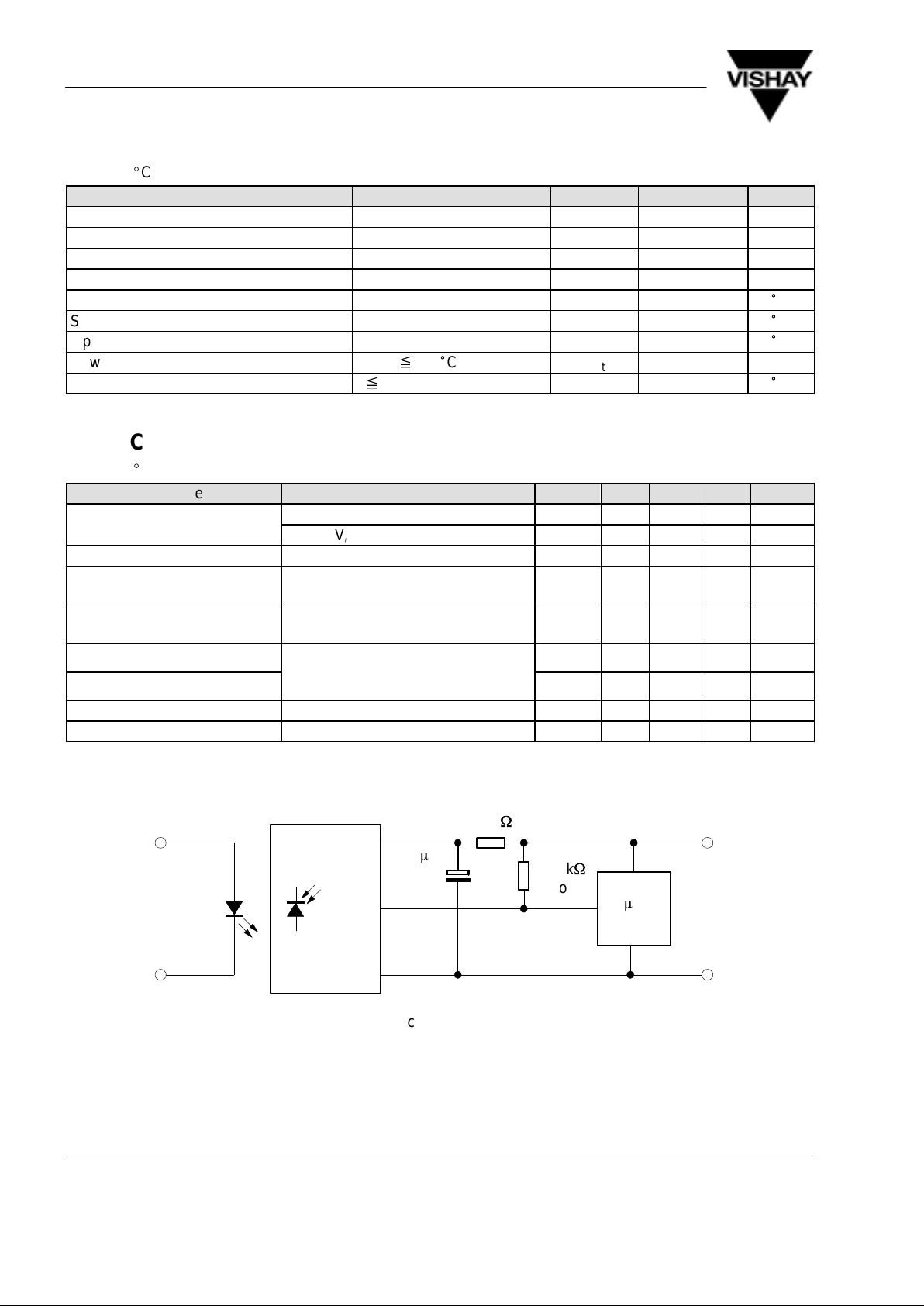
Absolute Maximum Ratings
T
amb
= 25_C
Parameter Test Conditions Symbol Value Unit
Supply Voltage (Pin 2) V
S
–0.3...6.0 V
Supply Current (Pin 2) I
S
5 mA
Output Voltage (Pin 1) V
O
–0.3...6.0 V
Output Current (Pin 1) I
O
5 mA
Junction Temperature T
j
100
°
C
Storage Temperature Range T
stg
–25...+85
°
C
Operating Temperature Range T
amb
–25...+85
°
C
Power Consumption (T
amb
x 85 °C) P
tot
50 mW
Soldering Temperature t x 10 s, 1 mm from case T
sd
260
°
C
Basic Characteristics
T
amb
= 25_C
Parameter Test Conditions Symbol Min Typ Max Unit
Supply Current (Pin 2) VS = 5 V, Ev = 0 I
SD
0.9 1.2 1.5 mA
y()
VS = 5 V, Ev = 40 klx, sunlight I
SH
1.3 mA
Supply Voltage (Pin 2) V
S
4.5 5.5 V
Transmission Distance Ev = 0, test signal see fig.6,
IR diode TSAL6200, I
F
= 300 mA
d 35 m
Output Voltage Low (Pin 1) IOL = 0.5 mA,Ee = 0.7 mW/m2,
f = f
o
V
OL
250 mV
Irradiance (30 – 40 kHz) Pulse width tolerance:
E
e min
0.3 0.5 mW/m
2
Irradiance (56 kHz)
t
pi
–
4/f
o
<
t
po
<
t
pi
+
6/f
o
,
test signal see fig.6
E
e min
0.4 0.7 mW/m
2
Irradiance E
e max
30 W/m
2
Directivity Angle of half transmission distance ϕ
1/2
±45 deg
Application Circuit
14319
TSAL62..
TSOP28..
2
1
3
4.7 mF *)
m
C
>10 k
W
optional
100 W *)
+5V
*) recommended to suppress power supply disturbances
GND
Page 3
TSOP28..
Vishay Telefunken
3 (7)Rev. 7, 31-Jan-00
www.vishay.de • FaxBack +1-408-970-5600
Document Number 82058
Suitable Data Format
The circuit of the TSOP28... is designed in that way
that unexpected output pulses due to noise or
disturbance signals are avoided. A bandpassfilter, an
integrator stage and an automatic gain control are
used to suppress such disturbances.
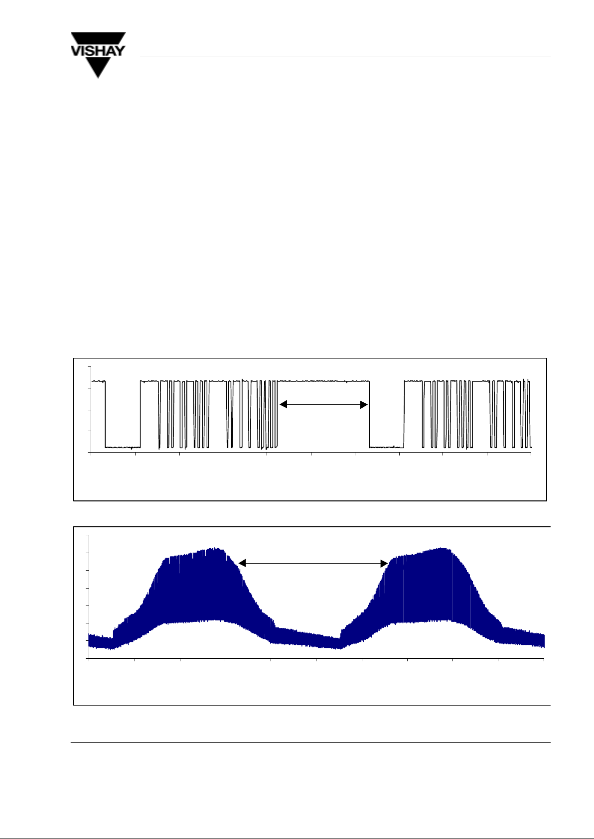
The distinguishing mark between data signal ( not
suppressed) and disturbance signal (supressed) are
carrier frequency, burst length and Signal Gap Time
(see diagram below).
The data signal should fullfill the following condition:
• Carrier frequency should be close to center
frequency of the bandpass (e.g. 38kHz).
• Burst length should be 6 cycles/burst or longer.
• After each burst a gap time of at least 10 cycles is
neccessary.
• The data format should not make a continuous
signal transmission. There must be a Signal Gap Time
(longer than 15ms) at least each 90ms (see Figure A).
Some examples for suitable data format are:
NEC Code (repetitive pulse), NEC Code (repetitive
data), Toshiba Micom Format, Sharp Code, RC5
Code, RECS–80 Code, R–2000 Code.
When a disturbance signal is applied to the TSOP28...
it can still receive the data signal. However the
sensitivity is reduced to that level that no unexpected
pulses will occure.
Some examples for such disturbance signals which
are suppressed by the TSOP28... are:
• DC light (e.g. from tungsten bulb or sunlight),
• Continuous signal at 38kHz or at any other
frequency,
• Signals from fluorescent lamps (see Figure B).
• Continuous IR signal (e.g. 1ms burst, 2ms pause)
0 102030405060708090100
time [ms]
Signal Gap Time
Figure A: Data Signal (Output of IR Receiver) with a Signal Gap Time of 20ms
0 2 4 6 8101214161820
time [ms]
Signal Gap Time
Figure B: Disturbance Signal from Fluorescent Lamp with Signal Gap Time of 7ms (suppressed by TSOP28..)
Page 4
TSOP28..
Vishay Telefunken
Rev. 7, 31-Jan-00
www.vishay.de • FaxBack +1-408-970-5600
Document Number 82058
4 (7)
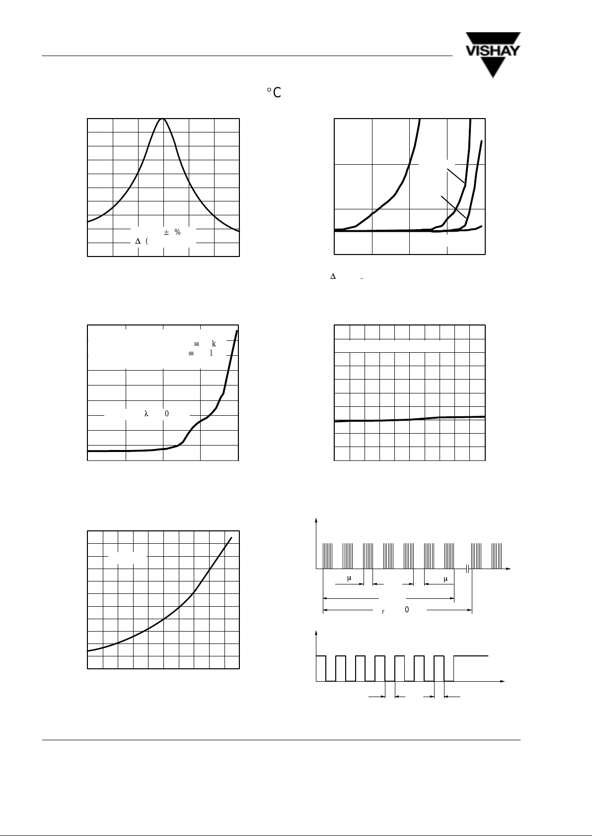
Typical Characteristics (T
amb
= 25_C unless otherwise specified)
0.7 0.8 0.9 1.0 1.1
E / E – Rel. Responsitivity
e min
f/f0 – Relative Frequency
1.3
94 9102
0.0
0.2
0.4
0.6
0.8
1.0
e
1.2
f = f0"
5%
D
f ( 3dB ) = f
0
/7
Figure 1. Frequency Dependence of Responsivity
0
0.5
1.0
1.5
2.0
2.5
3.0
3.5
4.0
4.5
0.01 0.10 1.00 10.00 100.00
E – DC Irradiance (W/m2)14310
e min
E – Threshold Irradiance (mW/m )
2
Correlation with ambient light sources
(Disturbance effect):10W/m2^1.4klx
(Stand.illum.A,T =2855K)^8.2klx
(Daylight,T =5900K)
Ambient, l = 950 nm
Figure 2. Sensitivity in Bright Ambient
0.0 0.4 0.8 1.2 1.6
0.0
0.4
0.8
1.2
2.0
E – Field Strength of Disturbance ( kV/m )
2.0
94 8147
1.6
E – Threshold Irradiance ( mW/m )
e min
2
f(E)=f
0
Figure 3. Sensitivity vs. Electric Field Disturbances
0.1
1.0
10.0
100.0
0.1 1.0 10.0 100.0 1000.0
D
V
sRMS –
AC Voltage on DC Supply Voltage (mV)
96 12215
e min
E – Threshold Irradiance (mW/m )
2
f = f
o
10 kHz
1 kHz
100 Hz
Figure 4. Sensitivity vs. Supply Voltage Disturbances
0
0.1
0.2
0.3
0.4
0.5
0.6
0.7
0.8
0.9
1.0
4.5 4.6 4.7 4.8 4.9 5.0 5.1 5.2 5.3 5.4 5.5
VS – Supply Voltage ( V )14312
e min
E – Threshold Irradiance (mW/m )
2
Sensitivity in dark ambient
Figure 5. Sensitivity vs. Supply Voltage
E
e
t
V
O
V
OH
V
OL
t
600 ms
600 ms
T
rep
=100 ms
T
on
T
off
15808
Optical Test Signal
Output Signal, ( see Fig.7 )
TD*
* T
rep–TD
> 15 ms is recommended for optimal function
Figure 6. Output Function
Page 5
TSOP28..
Vishay Telefunken
5 (7)Rev. 7, 31-Jan-00
www.vishay.de • FaxBack +1-408-970-5600
Document Number 82058
0.4
0.45
0.50
0.55
0.60
0.65
0.70
0.75
0.80
0.1 1.0 10.0 100.0 1000.010000.0100000.0
Ee – Irradiance (mW/m2)
16163
on off
T ,T – Output Pulse Length (ms)
T
on
optical test signal, fig.6
T
off
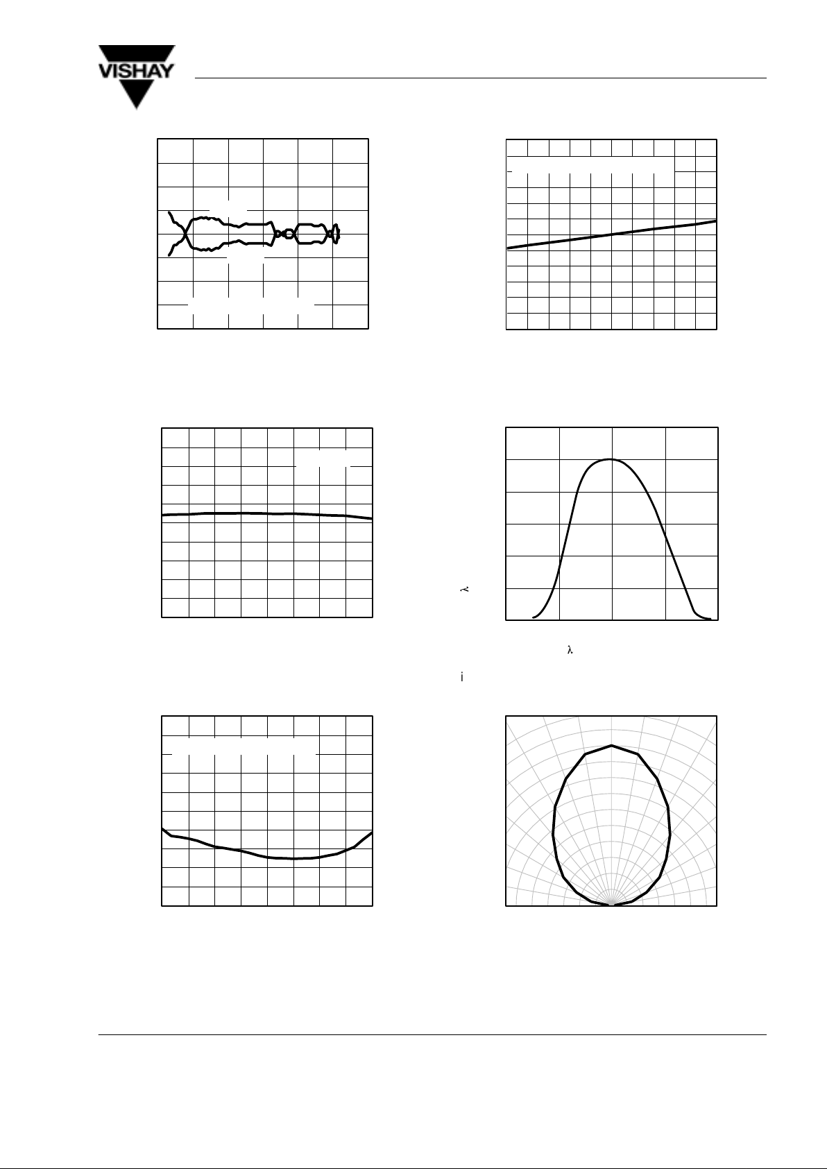
Figure 7. Output Pulse Diagram
0
0.2
0.4
0.6
0.8
1.0
1.2
1.4
1.6
1.8
2.0
–30 –15 0 15 30 45 60 75 90
T
amb
– Ambient Temperature ( °C )14315
I – Supply Current ( mA )
s
Vs = 5 V
Figure 8. Supply Current vs. Ambient Temperature
0
0.1
0.2
0.3
0.4
0.5
0.6
0.7
0.8
0.9
1.0
–30 –15 0 15 30 45 60 75 90
T
amb
– Ambient Temperature ( °C )96 12221
e min
E – Threshold Irradiance (mW/m )
2
Sensitivity in dark ambient
Figure 9. Sensitivity vs. Ambient Temperature
0.5
0.6
0.7
0.8
0.9
1.0
1.1
1.2
1.3
1.4
1.5
1.6
1.7
4.5 4.6 4.7 4.8 4.9 5.0 5.1 5.2 5.3 5.4 5.5
VS – Supply Voltage ( V )14317
I – Supply Current ( mA )
s
Supply current in dark ambient
Figure 10. Supply Current vs. Supply Voltage
750 850 950 1050
0
0.2
0.4
0.6
0.8
1.2
S ( ) – Relative Spectral Sensitivity
rel
l
– Wavelength ( nm )
1150
94 8408
1.0
l
Figure 11. Relative Spectral Sensitivity vs. Wavelength
96 12223p2
0.4 0.2 0 0.2 0.4
0.6
0.6
0.9
0°
30°
10° 20°
40°
50°
60°
70°
80°
1.0
0.8
0.7
d
rel
– Relative Transmission Distance
Figure 12. Directivity
Page 6
TSOP28..
Vishay Telefunken
Rev. 7, 31-Jan-00
www.vishay.de • FaxBack +1-408-970-5600
Document Number 82058
6 (7)
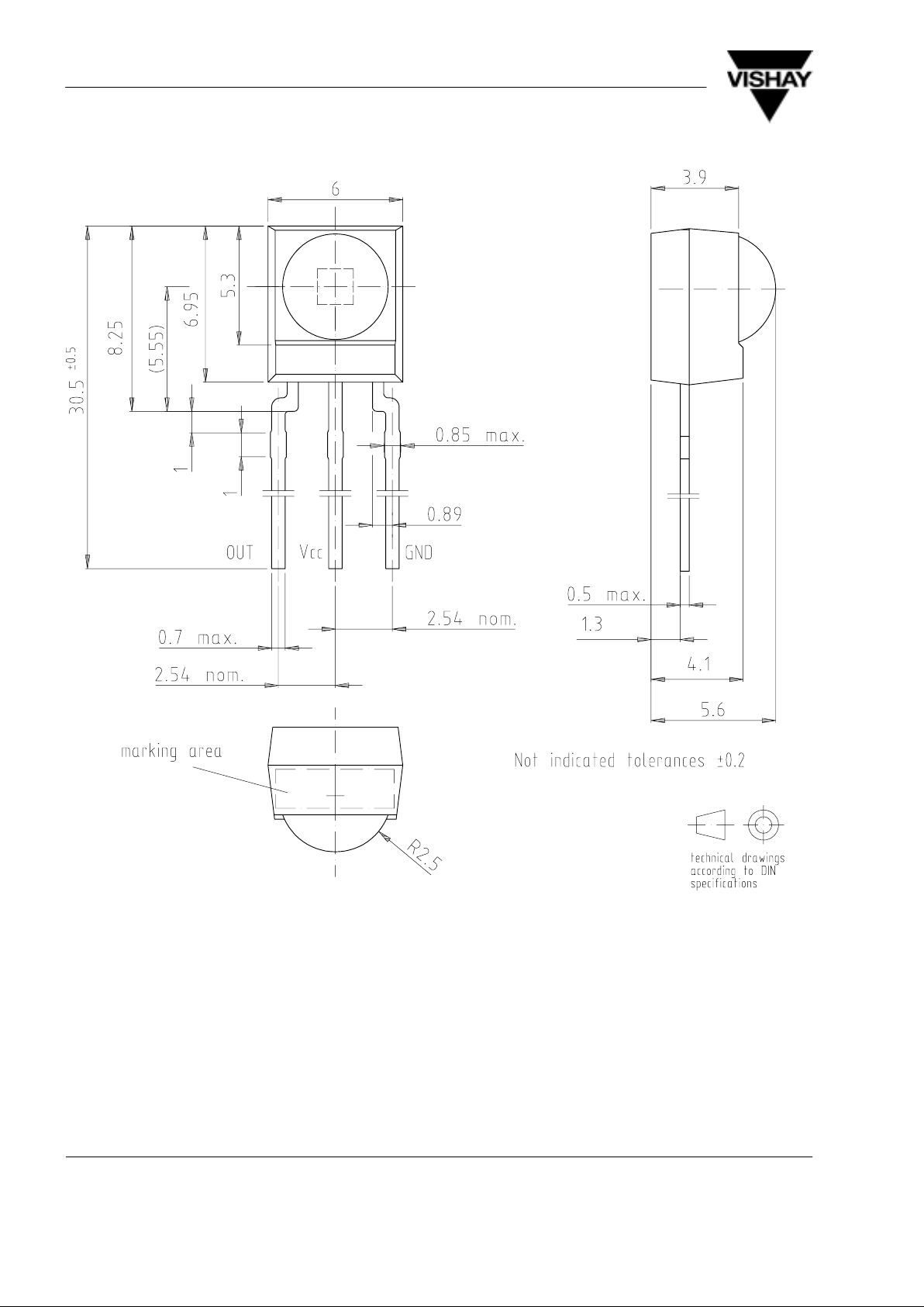
Dimensions in mm
13655
Page 7

TSOP28..
Vishay Telefunken
7 (7)Rev. 7, 31-Jan-00
www.vishay.de • FaxBack +1-408-970-5600
Document Number 82058
Ozone Depleting Substances Policy Statement
It is the policy of Vishay Semiconductor GmbH to
1. Meet all present and future national and international statutory requirements.
2. Regularly and continuously improve the performance of our products, processes, distribution and operating
systems with respect to their impact on the health and safety of our employees and the public, as well as their
impact on the environment.
It is particular concern to control or eliminate releases of those substances into the atmosphere which are known as
ozone depleting substances (ODSs).
The Montreal Protocol (1987) and its London Amendments (1990) intend to severely restrict the use of ODSs and
forbid their use within the next ten years. V arious national and international initiatives are pressing for an earlier ban
on these substances.
Vishay Semiconductor GmbH has been able to use its policy of continuous improvements to eliminate the use of
ODSs listed in the following documents.
1. Annex A, B and list of transitional substances of the Montreal Protocol and the London Amendments respectively
2.Class I and II ozone depleting substances in the Clean Air Act Amendments of 1990 by the Environmental
Protection Agency (EPA) in the USA
3. Council Decision 88/540/EEC and 91/690/EEC Annex A, B and C (transitional substances) respectively.
Vishay Semiconductor GmbH can certify that our semiconductors are not manufactured with ozone depleting
substances and do not contain such substances.
We reserve the right to make changes to improve technical design and may do so without further notice.
Parameters can vary in different applications. All operating parameters must be validated for each customer application
by the customer. Should the buyer use Vishay-Telefunken products for any unintended or unauthorized application, the
buyer shall indemnify Vishay-Telefunken against all claims, costs, damages, and expenses, arising out of, directly or
indirectly , any claim of personal damage, injury or death associated with such unintended or unauthorized use.
Vishay Semiconductor GmbH, P.O.B. 3535, D-74025 Heilbronn, Germany
Telephone: 49 (0)7131 67 2831, Fax number: 49 (0)7131 67 2423
 Loading...