

Page 1
TSM260P02
FEATURES
● Fast switching
● Suitable for -1.8V Gate Drive Applications
● Pb-free plating
● RoHS compliant
● Halogen-free mold compound
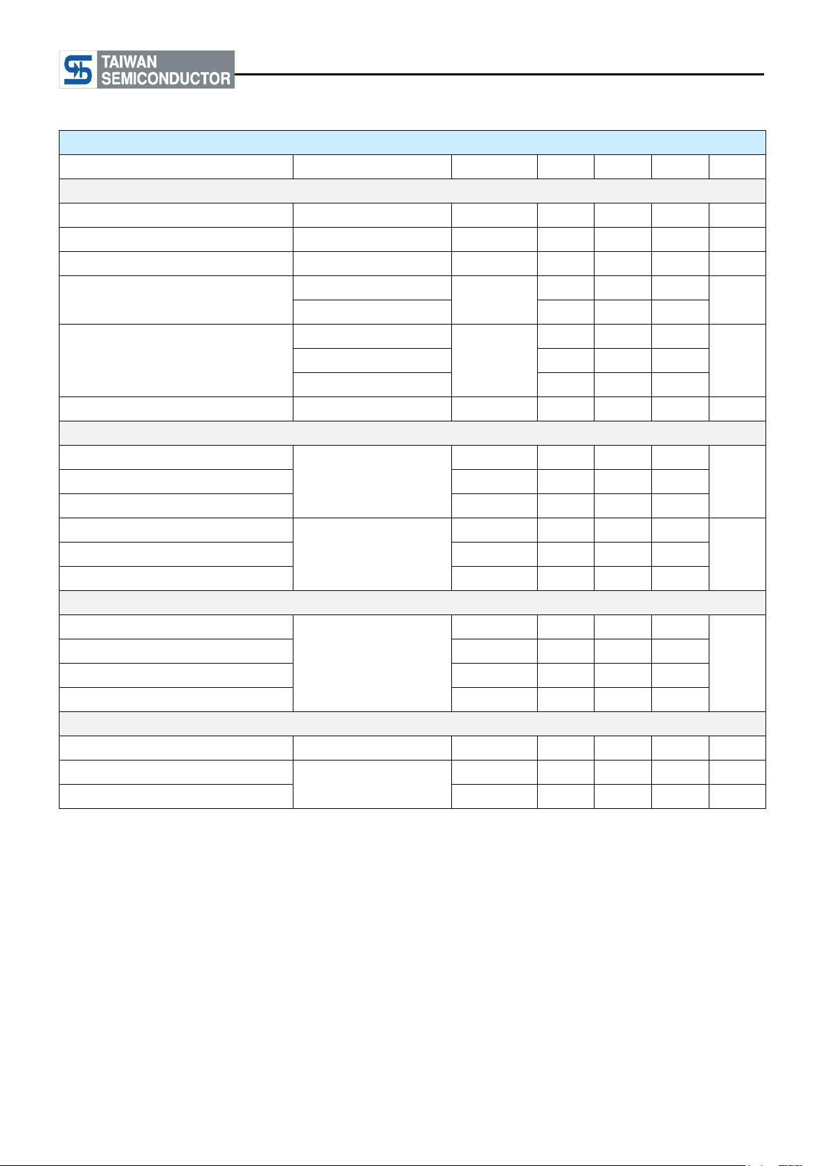
KEY PERFORMANCE PARAMETERS
PARAMETER
VALUE
UNIT
VDS
-20
V
ID
-6.5
A
R
DS(on)
(max)
VGS = -4.5V
26
mΩ
VGS = -2.5V
32
VGS = -1.8V
40
Qg
19.5
nC
APPLICATION
● Battery Pack
● Portable Devices
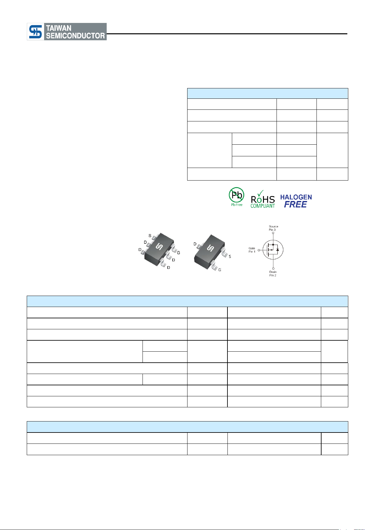
SOT-26
SOT-23
ABSOLUTE MAXIMUM RATINGS (T
A
= 25°C unless otherwise noted)
PARAMETER
SYMBOL
LIMIT
UNIT
Drain-Source Voltage
VDS
-20
V
Gate-Source Voltage
VGS
±10
V
Continuous Drain Current
TC = 25°C
ID
-6.5
A
TC = 100°C
-4.1
Pulsed Drain Current
(Note 1)
IDM
-26
A
Total Power Dissipation
TC = 25°C
P
DTOT
1.56
W
Operating Junction Temperature
TJ
150
ºC
Operating Junction and Storage Temperature Range
TJ, T
STG
- 55 to +150
°C
THERMAL PERFORMANCE
PARAMETER
SYMBOL
LIMIT
UNIT
Junction to Ambient Thermal Resistance
R
ӨJA
80
°C/W
Taiwan Semiconductor
P-Channel Power MOSFET
-20V, -6.5A, 26mΩ
Notes: Moisture sensitivity level: level 3. Per J-STD-020
Notes: R
R
is determined by the user’s board design. R
ӨCA
Document Number: DS_P0000208 1 Version: B15
is the sum of the junction-to-case and case-to-ambient thermal resistances. R
ӨJA
is guaranteed by design while
ӨJA
is shown for single device operation on FR-4 PCB in still air.
ӨJA
Page 2
TSM260P02
ELECTRICAL SPECIFICATIONS (T
A
= 25°C unless otherwise noted)
PARAMETER
CONDITIONS
SYMBOL
MIN
TYP
MAX
UNIT
Static
(Note 2)
Drain-Source Breakdown Voltage
V
GS
= 0V, ID = -250µA
BV
DSS
-20
--
--
V
Gate Threshold Voltage
V
DS
= VGS, ID = -250µA
V
GS(TH)
-0.3
-0.6
-1.0
V
Gate Body Leakage
VGS = ±10V, VDS = 0V
I
GSS
--
--
±100
nA
Zero Gate Voltage Drain Current
V
DS
= -20V, VGS = 0V
I
DSS
--
--
-1
µA
V
DS
= -16V, TJ = 125ºC
--
--
-10
Drain-Source On-State Resistance
V
GS
= -4.5V, ID = -5A
R
DS(on)
--
21
26
mΩ
V
GS
= -2.5V, ID = -4A
--
26
32
V
GS
= -1.8V, ID = -3A
--
32
40
Forward Transconductance
V
DS
= -10V, IS = -5A
gfs
--
15
--
S
Dynamic
(Note 3)
Total Gate Charge
V
DS
= -10V, ID = -5A,
V
GS
=- 4.5V
Qg
--
19.5
--
nC
Gate-Source Charge
Qgs
-- 2 --
Gate-Drain Charge
Qgd
--
3.6
--
Input Capacitance
V
DS
= -15V, VGS = 0V,
F = 1.0MHz
C
iss
--
1670
--
pF
Output Capacitance
C
oss
--
220
--
Reverse Transfer Capacitance
C
rss
--
120
--
Switching
Turn-On Delay Time
V
DD
= -10V, ID = -1A,
VGS = -4.5V, R
GEN
=25Ω
t
d(on)
--
10.4
--
ns
Turn-On Rise Time
tr
--
37.5
--
Turn-Off Delay Time
t
d(off)
--
89.1
--
Turn-Off Fall Time
tf
--
24.6
--
Source-Drain Diode
Forward Voltage
VGS = 0V, IS = -1A
VSD
--
--
-1
V
Continuous Forward Current
Integral reverse diode
in the MOSFET
IS
--
--
-6.5
A
Pulse Forward Current
ISM
--
--
-26
A
Taiwan Semiconductor
Notes:
1. Pulse width limited by safe operating area
2. Pulse test: PW ≤ 300µs, duty cycle ≤ 2%
3. Switching time is essentially independent of operating temperature.
Document Number: DS_P0000208 2 Version: B15
Page 3

TSM260P02
PART NO.
PACKAGE
PACKING
TSM260P02CX RFG
SOT-23
3,000pcs / 7” Reel
TSM260P02CX6 RFG
SOT-26
3,000pcs / 7” Reel
ORDERING INFORMATION
Note:
1. Compliant to RoHS Directive 2011/65/EU and in accordance to WEEE 2002/96/EC
2. Halogen-free according to IEC 61249-2-21 definition
Taiwan Semiconductor
Document Number: DS_P0000208 3 Version: B15
Page 4

TSM260P02
Continuous Drain Current vs. TC
Gate Charge
On-Resistance vs. Junction Temperature
Threshold Voltage vs. Junction Temperature
Maximum Safe Operating Area
Normalized Thermal Transient Impedance Curve
Square Wave Pulse Duration (s)
-V
, Drain to Source Voltage (V)
TJ, Junction Temperature (°C)
TJ, Junction Temperature (°C)
Qg, Gate Charge (nC)
TC, Case Temperature (°C)
-VGS, Gate to Source Voltage (V)
-I
D
, Continuous Drain Current (A)
Normalized On Resistance (mΩ)
Normalized Gate Threshold Voltage
Normalized Thermal Response (R
ӨJA
)
-I
D
, Continuous Drain Current (A)
CHARACTERISTICS CURVES
(TC = 25°C unless otherwise noted)
Taiwan Semiconductor
Document Number: DS_P0000208 4 Version: B15
Page 5
TSM260P02
26
= Device Code
Y
= Year Code
M
= Month Code for Halogen Free Product
O
=Jan
P
=Feb
Q
=Mar
R
=Apr S =May
T
=Jun
U
=Jul
V
=Aug
W
=Sep
X
=Oct
Y
=Nov
Z
=Dec
L
= Lot Code
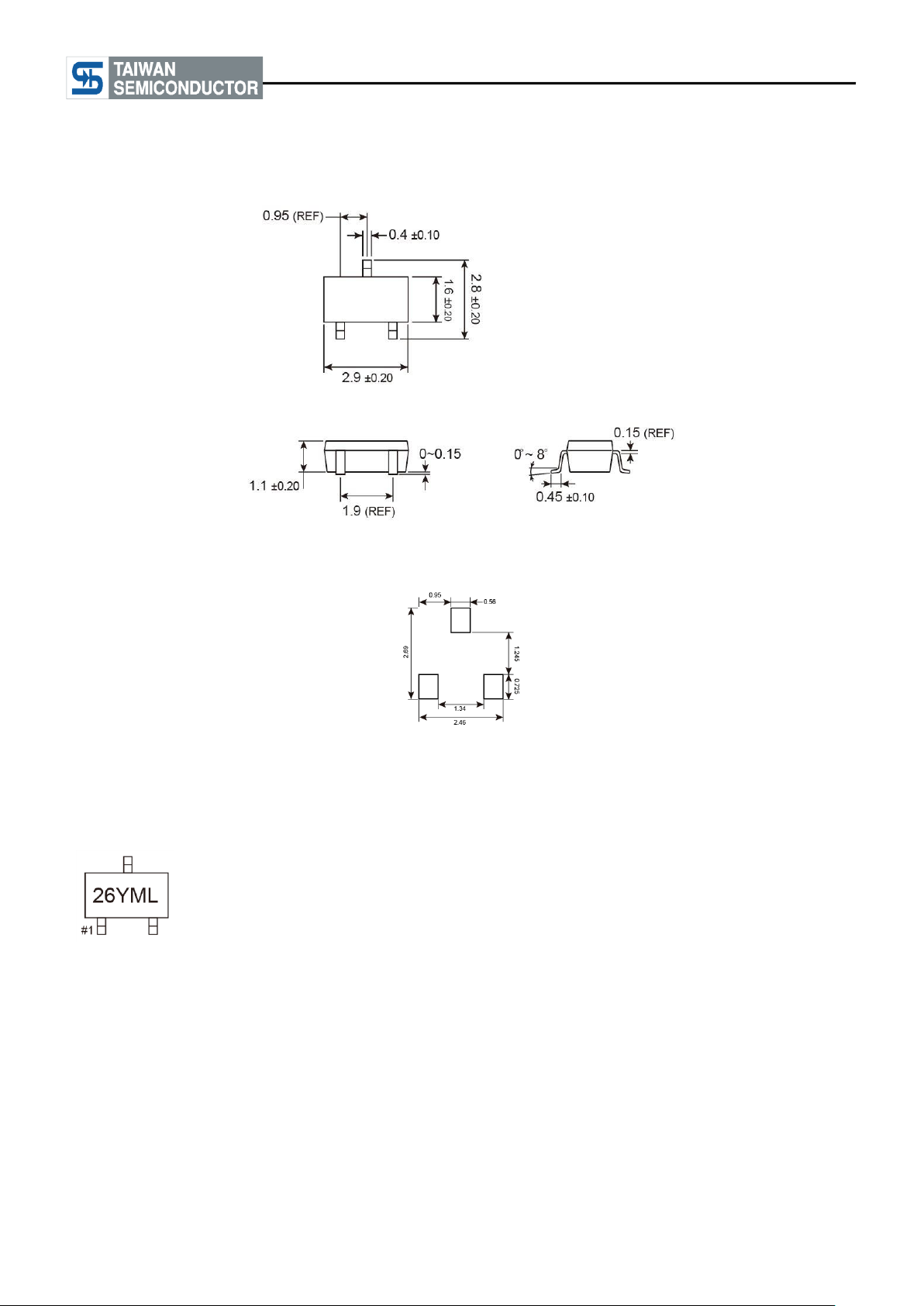
PACKAGE OUTLINE DIMENSIONS (Unit: Millimeters)
SOT-23
SUGGESTED PAD LAYOUT (Unit: Millimeters)
Taiwan Semiconductor
MARKING DIAGRAM
Document Number: DS_P0000208 5 Version: B15
Page 6

TSM260P02
26
= Device Code
Y
= Year Code
M
= Month Code for Halogen Free Product
O
=Jan
P
=Feb
Q
=Mar
R
=Apr
S
=May
T
=Jun
U
=Jul
V
=Aug
W
=Sep
X
=Oct
Y
=Nov
Z
=Dec
L
= Lot Code (1~9, A~Z)
PACKAGE OUTLINE DIMENSIONS (Unit: Millimeters)
SOT-26
Taiwan Semiconductor
SUGGESTED PAD LAYOUT (Unit: Millimeters)
MARKING DIAGRAM
Document Number: DS_P0000208 6 Version: B15
Page 7

TSM260P02
Taiwan Semiconductor
Notice
Specifications of the products displayed herein are subject to change without notice. TSC or anyone on its behalf,
assumes no responsibility or liability for any errors or inaccuracies.
Information contained herein is intended to provide a product description only. No license, express or implied, to
any intellectual property rights is granted by this document. Except as provided in TSC’s terms and conditions of
sale for such products, TSC assumes no liability whatsoever, and disclaims any express or implied warranty,
relating to sale and/or use of TSC products including liability or warranties relating to fitness for a particular purpose,
merchantability, or infringement of any patent, copyright, or other intellectual property right.
The products shown herein are not designed for use in medical, life-saving, or life-sustaining applications.
Customers using or selling these products for use in such applications do so at their own risk and agree to fully
indemnify TSC for any damages resulting from such improper use or sale.
Document Number: DS_P0000208 7 Version: B15
Page 8

 Loading...