

Page 1
TSM109/A
Dual Comparator and Voltage Reference
COMPARATOR
■ Low supply current (1.1ma) independent of
supply voltage
■ Low input bias current: 25nA typ
■ Low input offset voltage: ±1mV typ
■ Input common-mode voltage ran ge
includes ground
■ Low output saturation voltage: 250mV typ
(Io = 4mA)
■ Differential input voltage range equal to the
supply voltage
■ Wide po wer supply range: ±1V to ±18V
VOLTAGE REFERENCE
■ Fixed V
■ 0.4% and 1% voltage precision
■ Sink current capability: 1 to 100mA
to 2.5V
ref
DESCRIPTION
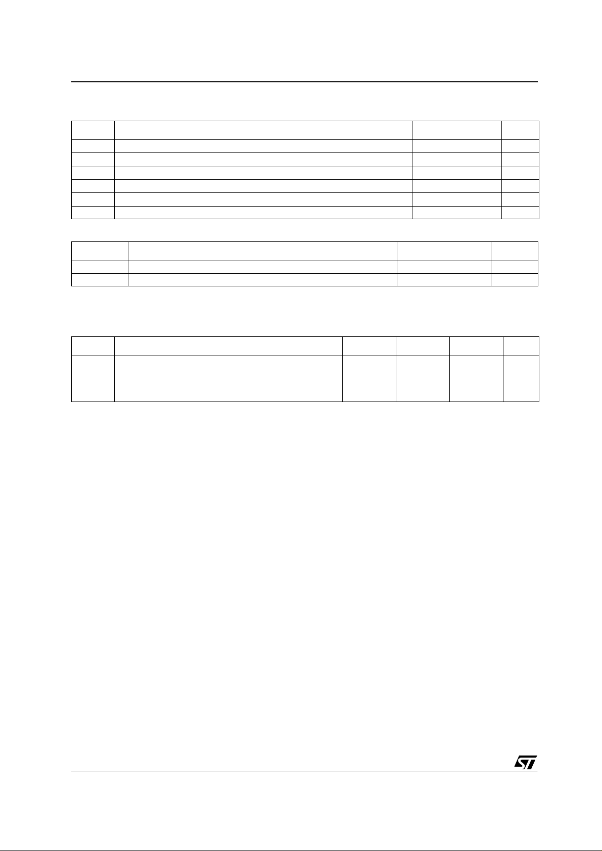
The TSM109 is a monolithic IC that includes two
comparators and a shunt voltage refe rence. This
device offers space and cost savings in many
applications including power supply management
or data acquisition systems.
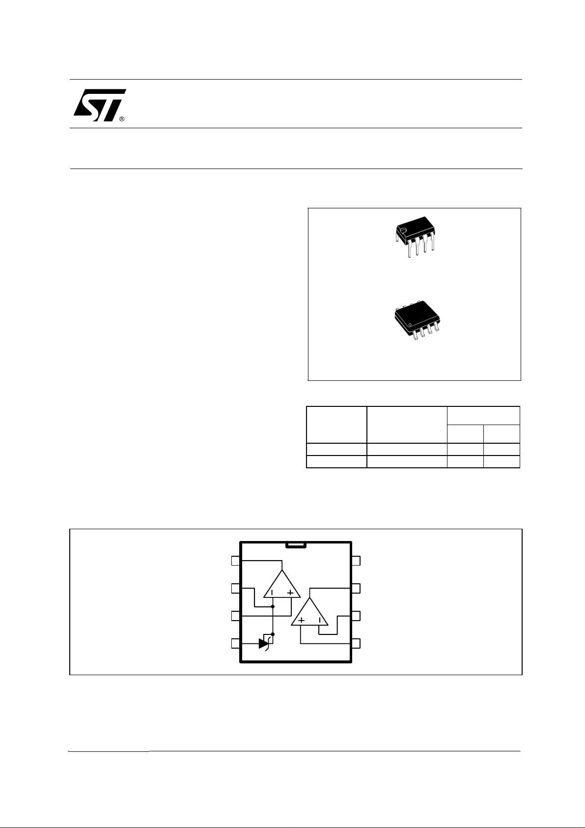
Package Reference
N
DIP-8
D
SO-8
ORDER CODE
Part
Number
TSM109 -40°C, +105°C ••
TSM109A -40°C, +105°C ••
Note: N = Dual in Line Package (DI P)
D = Smal l Ou tlin e Pa ckag e (S O) - a lso avai la ble in T ape &
Reel (DT)
Temperature
Range
Package
ND
PIN C ONNECTIONS (top view)
February 2004
Out
1
Vref
2
Ve+
3
Gnd
4
Vcc
Out
Ve-
Ve+
8
7
6
5
1/7
Page 2
TSM109/A Absolute Maximum Ratings
1 ABSOLUTE MAXIMUM RATINGS
Symbol Parameter Value
VCC Supply voltage 36 V
Input Voltage -0.3 to V
Vin
Ik Continuous Cathode current range -100 to 150 mA
Maximum Junction Temperature
T
j
R
ESD Electrostatic Discharge Protection 1.5 kV
OPERATING CONDITIONS
Thermal Resistance Junction to Ambient (SO package)
thja
+0.3
cc
150 °C
175 °C/W
Symbol Parameter Value Unit
Vcc DC Supply Conditions 2 to 36 V
Toper Operational temp eratur e -40 to105 °C
ELECTRICAL CHARACTERISTICS
+
V
= 5V, V
CC
Symbol Parameter Min Typ Max
Total Supply Current, excluding current in the Voltage
I
CC
Reference
V
V
-
= 0V, T
CC
= +5V, no load
CC
= +30V, no load
CC
= 25°C (unless otherwise specified)
amb
0.4
1
1
2.5
Unit
V
Unit
mA
2/7
Page 3
Electrical Characteristics TSM109/A
2 ELECTRICAL CHARACTERISTICS
COMPARATOR (independent comparator)
+
= +5V, V
V
CC
Symbo
l
Input Offset Voltage - note 1
V
T
io
amb
T
min
Input Offset Current
T
I
I
A
V
V
V
I
OH
I
sink
t
t
1) At output switch point, Vo ≈ 1.4V, Rs = 0 with V
2) The direct ion of the inp ut cur re nt is out of the IC due to th e PNP inpu t stage . This curre nt is esse ntial ly cons tan t, in depen dent of t he
3) The input common-mode voltage of either input signal voltage should not be allowed to go negative by more than 0.3V. The upper end
4) Positive v oltage e xcursi ons of one inp ut may e xceed t he power supply level. A s long as the other inp ut vol tage rema ins wit hin the
5) The response time specified is for a 100mV input step with 5mV overdrive. For larger overdrive signals, 300ns can be obtained
amb
io
T
min
Input Bias Current (I+ or I-) - note
T
ib
amb
T
min
Large Signal Voltage Gain
vd
V
CC
Input Common Mode Voltage Range - note
V
CC
icm
T
amb
T
min
Differential Input Voltage -note
id
Low Level Output Voltage
V
id
OL
T
amb
T
min
High Level Output Current (Vid = 1V)
V
CC
T
amb
T
min
Output Sink Currrent
V
id
Response Time - note 5
re
R
Large Signal Response Time
R
rel
V
state of the output, so no lo ading charge exists on the reference of input lines.
of the comm on-mode voltage range is V
common-mode range, the comparator will provide an a ppropriate output st ate. The low input v oltage state mu st not be less than -0.3V
(or 0.3V below the negative power supply, if used).
-
= GND, T
CC
= +25°C (unless otherwise specified)
amb
= +25°C
≤ T
≤ T
amb
max
= +25°C
≤ T
≤ T
amb
max
= +25°C
≤ T
≤ T
amb
= 15V, RL = 15kΩ, Vo = 1V to 11V
= 30V
max
= +25°C
≤ T
≤ T
amb
= -1V, I
sink
max
= 4mA
= +25°C
≤ T
≤ T
amb
= Vo = 30V
max
= +25°C
≤ T
≤ T
amb
max
= 1V, Vo = 1.5V
= 5.1kΩ connected to V
L
= 5.1kΩ connected to V
L
= +1.4v
(ref)
+
CC
+
, el = TTL,
CC
CC
Parameter
Min. Typ. Max.
2
3
4
+
from 5V to 30V, and over the full common-mode ran ge (0V to V
CC
+
-1.5V.
TSM109
Unit
159mV
325
100
25 250
400
50 200 V/mV
+
0
0
V
CC
V
CC
V
CC
250 400
700
30 150
1
10 20 mA
1.3 µs
300 ns
+
CC
-1.5
+
-2
+
-1.5V).
nA
nA
V
mV
nA
µA
3/7
Page 4

TSM109/A Electrical Characteristics
COMPARATOR (comparator with inverting input connected to the internal Vref))
+
V
= +5V, V
CC
Symbo
l
Input Offset Voltage - note 1
V
T
io
amb
T
min
Input Bias Current for positive input note
I
T
ib
amb
T
min
Large Signal Voltage Gain
A
vd
V
CC
Differential Input Voltage -note
V
id
Low Level Output Voltage
V
V
I
OH
I
sink
t
t
1) At output switch point, Vo ≈ 1.4V, Rs = 0 with V
2) The direct ion of the inp ut cur re nt is out of the IC due to th e PNP inpu t stage . This curre nt is esse ntial ly cons tan t, in depen dent of t he
3) The respo nse time specified is for a 100mV input step with 5mV overdrive. Fo r l arger overd ri ve signals, 30 0ns can be obt ai ned.
id
OL
T
amb
T
min
High Level Output Current (Vid = 1V)
V
CC
T
amb
T
min
Output Sink Currrent
V
id
Response Time - note 3
re
R
Large Signal Response Time
RL= 5.1kΩ connected to V
rel
V
state of the output, so no lo ading charge exists on the reference of input lines.
-
= GND, T
CC
= +25°C (unless otherwise specified)
amb
= +25°C
≤ T
≤ T
amb
max
= +25°C
≤ T
≤ T
amb
= 15V, RL = 15kΩ, Vo = 1V to 11V
= -1V, I
sink
max
= 4mA
= +25°C
≤ T
≤ T
amb
= Vo = 30V
max
= +25°C
≤ T
≤ T
amb
max
= 1V, Vo = 1.5V
= 5.1kΩ connected to V
L
= +1.4v
(ref)
+
CC
+
, el = TTL,
CC
Parameter
Min. Typ. Max.
2
+
from 5V to 30V, and over the full common-mode ran ge (0V to V
CC
TSM109
Unit
159mV
25 250
400
50 200 V/mV
V
CC
-2.5V
250 400
700
30 150
1
10 20 mA
1.3 µs
300 ns
+
CC
nA
+
V
mV
nA
µA
-1.5V).
4/7
Page 5

Electrical Characteristics TSM109/A
ELECTRICAL CHARACTERISTICS
VOLTAGE REFERENCE
Symbol Conditions Value Unit
I
Cathode Current
K
T
= 25°C (unless otherwise specified)
amb
Symbo
l
Parameter
Reference Input Voltage, IK = 10 mA
T
T
amb
min
= 25°C
≤ T
amb
≤ T
max
V
ref
Reference Input Voltage Deviation OverT emperature
∆V
ref
Range I
T
min
≤T
= 10 mA
K
≤ T
amb
max
Temperature Coefficient of Reference Input Voltage
= 10 mA,
I
∆Vref
--------------------
Vref
I
|Z
1) The dyn am i c im pedance is defined as [Z
K
T
≤T
min
∆T
Minimum Cathode Current for Regulation
min
Dynamic Impedance - note
|
Vref
∆V
ref
≤ T
amb
max
, ∆IK = 1 to 100mA, f < 1KHz
Vref
1
| = ∆V
Vref
/∆I
TSM109A TSM109
Min. Typ. Max. Min. Typ. Max.
2.490
K
2.48
2.500 2.510
2.52
730 730mV
±13 ±90 ±13 ±90 ppm/°C
0.5 1 0.5 1 mA
0.3 0.65 0.3 0.65
1 to 100 mA
2.475
2.500 2.525
2.45
2.55
Unit
V
Ω
5/7
Page 6

TSM109/A PACKAGE MECHANICAL DATA
3 PACKAGE MECHANICAL DATA
Plastic DIP-8 MECHANICAL DATA
DIM.
A 3.3 0.130
a1 0.7 0.028
B 1.39 1.65 0.055 0.065
B1 0.91 1.04 0.036 0.041
b 0.5 0.020
b1 0.38 0.5 0.015 0.020
D 9.8 0.386
E 8.8 0.346
e 2.54 0.100
e3 7.62 0.300
e4 7.62 0.300
F 7.1 0.280
I 4.8 0.189
L 3.3 0.130
Z 0.44 1.6 0.017 0.063
MIN. TYP MAX. MIN. TYP. MAX.
mm. inch
6/7
P001F
Page 7

PACKAGE MECHANICAL DATA TSM109/A
PACKAGE MECHANICAL DATA
SO-8 MECHANICAL DATA
DIM.
A 1.35 1.75 0.053 0.069
A1 0.10 0.25 0.04 0.010
A2 1.10 1.65 0.043 0.065
B 0.33 0.51 0.013 0.020
C 0.19 0.25 0.007 0.010
D 4.80 5.00 0.189 0.197
E 3.80 4.00 0.150 0.157
e 1.27 0.050
H 5.80 6.20 0.228 0.244
h 0.25 0.50 0.010 0.020
L 0.40 1.27 0.016 0.050
k ˚ (max.)
ddd 0.1 0.04
MIN. TYP MAX. MIN. TYP. MAX.
mm. inch
8
0016023/C
Informat ion furnished is believed t o be accurate and reliable. H owever, STMicr oelectronics assumes no responsibility for the
consequences of use of such information nor for any infringement of patents or other rights of third parties which may result from
its use. No license is granted by implication or otherwise under any patent or patent rights of STMicroelectronics. Specifications
mentioned in this publication are subject to change without notice. This publicati on supersedes and replaces all information
previously supplied. STMicroe lectronics products are not au thorized for use as cr itical components in life s upport devices or
systems without express written approval of STMicroelectronics.
The ST logo is a registered trademark of STMicroelectronics
All other na mes are the prop erty of thei r respective o w ners.
© 2004 STM i cr o electron ics - All Righ ts Reserved
STMicroele ctronics GROUP OF C OM P AN IES
Austra l ia - Belgium - Brazil - Canada - China - Czech Republ i c - Fi nl and - France - Germany
Hong Kong - India - Isr ael - Italy - Japa n - M al aysia - Malt a - M orocco - Singapore - S pai n
Sweden - Sw i tz e rland - Un i te d Kingdom - Un i ted States
http://www.st.com
7/7
 Loading...