

Page 1
TSM104W/A
QUAD OPERATIONAL AMPLIFIER AND
PROGRAMMABLE VOLTAGE REFERENCE
OPERATIONAL AMPLIFIERS
■ LOW SUPPLY CURRENT : 375µA/op.
(@ VCC = 5V)
■ LOW INPUT BIAS CURRENT : 20nA
■ MEDIUM SPEED : 0.9MHz
■ LOW INPUT OFFSET VOLTAGE : 0.5 mV typ
for TSM104WA
■ WIDE POWER SUPPLY RANGE : ±1.5V to
±15V
■ 2kV ESD PROTECTION
VOLTAGE REFERENCE
■ ADJUSTABLE OUTPUT VOLTAGE :
V
to 36V
ref
■ 0.4% AND 1% VOLTAGE PRECISION
■ SINK CURRENT CAPABILITY : 1 to 100mA
■ TYPICAL OUTPUT IMPEDANCE : 0.2Ω
DESCRIPTION
The TSM104W is a monolithic IC that includes
four op-amps and an adjustable shunt voltage reference. This device is offering space and cost
saving in many applications like power supply
management or data acquisition systems.
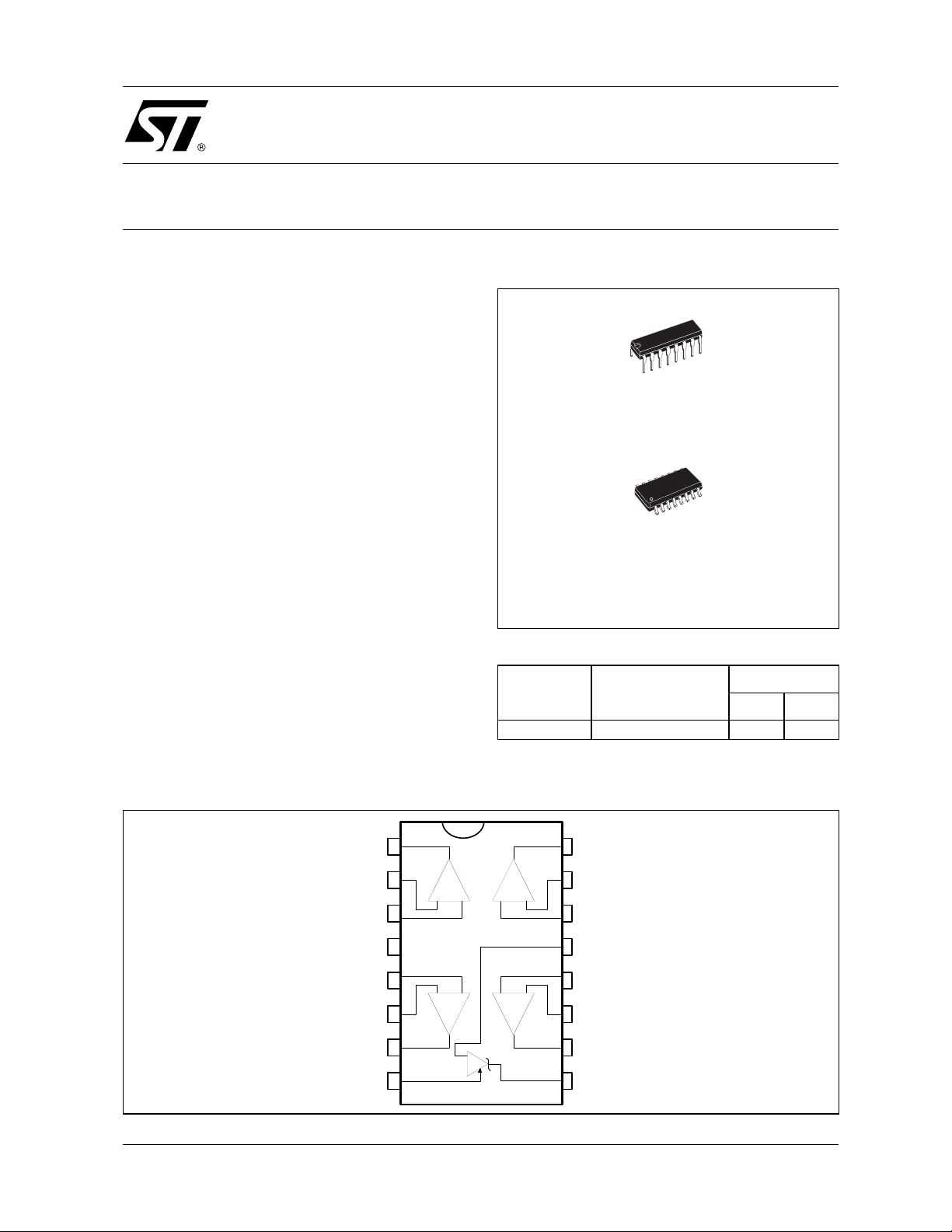
N
DIP16
(Plastic Package)
D
SO16
(Plastic Micropackage)
ORDER CODE
Part Number Temperature Range
TSM104WI/AI -40°C, +105°C
N = Dual in Line Package (DIP)
D = Small Outline Package (SO) - also available in Tape & Reel (DT)
Package
ND
••
PIN CONNECTIONS (top view)
Output 1
Inverting Input 1
Non-inverting Input 1
V
CC
Non-inverting Input 2
Inverting Input 2
Output 2
Adjust
January 2003
16
1
2
3
+
4
5
6
7
8
Output 4
Inverting Input
15
Non-inverting Input 4
14
V
-
13
CC
Non-inverting Input 3
12
Inverting Input 3
11
10
Output 3
9
Cathode
1/9
Page 2
TSM104W/A
ABSOLUTE MAXIMUM RATINGS
Symbol Parameter Value Unit
V
T
R
ESD Electrostatic Discharge Protection 2 kV
ELECTRICAL CHARACTERISTICS
V
CC
Symbol Parameter Min Typ Max Unit
Supply Voltage 36 V
CC
V
Differential Input Voltage 36 V
id
V
Input Voltage -0.3 to Vcc + 0.3 V
i
Output Short-circuit Duration Infinite
Operating Free-Air Temperature Range -55 to +125 °C
oper
T
Maximum Junction Temperature 150 °C
j
Thermal Resistance Junction to Ambient (SO package) 150 °C/W
thja
+
= 5V, V
I
CC
-
CC
= 0V, T
= 25°C (unless otherwise specified)
amb
Total Supply Current, excluding current in the Voltage
Reference
+
= 5V, no load
V
CC
T
< T
min.
+
V
CC
T
min.
< T
amb
max.
= 30V, no load
< T
< T
amb
max.
1.4 2.4
4
mA
2/9
Page 3
TSM104W/A
ELECTRICAL CHARACTERISTICS
+
V
= 5V, V
CC
Symbol Parameter Min. Typ. Max. Unit
V
io
V
∆
io
Iio
I
ib
A
vd
SVR
Vicm
CMR
I
source
I
o
I
sink
V
OH
V
OL
SR
GBP
THD
e
n
Cs
1. The input common-mode voltage of either input signal voltage should not be allowed to go negative by more than 0.3V. The upper end of the
common-mode voltage range is V
-
= Ground, VO = 1.4V, T
cc
= 25°C (unless otherwise specified)
amb
Input Offset Voltage
TSM104W, T
T
≤ T
min
amb
TSM104WA, T
T
≤ T
min
amb
amb
≤ T
≤ T
= 25°C
max
= 25°C
amb
max
0.5
Input Offset Voltage Drift 7
Input Offset Current
T
≤ T
amb
≤ T
max
min
Input Bias Current
≤ T
T
min
amb
≤ T
max
Large Signal Voltage Gain
V
= 15V, RL = 2k
CC
V
= 1.4V to 11.4V
O
T
≤ T
min
amb
≤ T
max
50
25
100
Supply Voltage Rejection Ratio
V
= 5V to 30V
CC
65 100
Input Voltage Mode Voltage Range
V
= + 30V see note1)
CC
T
≤ T
≤ T
min
amb
max
Common Mode Rejection Ratio
T
≤ T
amb
≤ T
max
min
0
0
70
60
Output Current Source
= 2V, V
V
o
= +15V, Vid = +1V
cc
20 40
Output Short Circuit to Ground
= +15V
V
CC
Output Current Sink
V
= -1V
id
V
= +15V, Vo = +2V 10 20 mA
CC
High Level Output Voltage
amb
amb
CC
≤ T
≤ T
+
= 30V
max
max
27
27
= 10k, V
R
L
T
= 25°C
amb
T
≤ T
min
Low Level Output Voltage
R
L
T
min
= 10k
≤ T
Slew Rate at Unity Gain
= 0.5 to 3V, V
V
i
R
= 2kΩ, CL = 100pF, unity gain
L
CC
= 15V
0.1 0.3
Gain Bandwith Product
= 30V, RL = 2k, CL = 100pF
V
CC
f = 100kHz, V
= 10mV
in
0.5 0.9
Total Harmonic Distortion
f = 1kHz
= 20dB, RL = 2, VCC = 30V
A
V
C
= 100pF, Vo = 2Vpp
L
0.02
Equivalent Input Noise Voltage
f = 1kHz, V
= 30V, Rs = 100
CC
Ω
Channel Separation
1kHz < f < 20kHz 120
+
-1.5V, but either of both inputs can go to Vcc+0.3V without damage.
CC
mV
1
5
6
3
4
V/°C
µ
23050nA
20 150
nA
200
V/mV
dB
V
Vcc+ -1.5
+
-2
Vcc
85 dB
mA
mA
40 60
V
28
mV
520
20
V/µs
MHz
%
50
nV
----------- Hz
dB
3/9
Page 4

TSM104W/A
VOLTAGE REFERENCE
Symbol Conditions Value Unit
I
Cathode Current 1 to 100 mA
k
Symbol Parameter Min Typ Max Unit
Reference Input Voltage
TSM104W, T
T
V
ref
min
≤ T
amb
TSM104WA, T
T
≤ T
min
amb
Reference Input Voltage Deviation Over Temperature Range
= V
V
∆
ref
V
∆
ref
---------------V
∆
KA
V
KA
min
≤ T
ref
amb
T
Ratio of Change in Reference Input Voltage to Charge in
Cathode to Anode Voltage
= 10mA, ∆VKA =36V to 3V
I
K
Reference Input Current
I
I
ref
I
∆
I
Z
1) The dyn amic impedance is defined a s
Reference Input Current Deviation over T° Range 0.8 1.2
ref
Minimum Cathode Current for Regulation
min
I
Off-State Cathode Current 180 500 nA
off
Dynamic Impedance - note 1
KA
= 10mA
K
T
min
V
KA
V
KA
≤ T
= V
= V
amb
ref
ref
= 25°C
amb
≤ T
max
= 25°C
amb
≤ T
max
, IK = 10mA
≤ T
max
≤ T
max
, ∆IK = 1 to 100mA, f < 1kHz
∆V
Z
KA
KA
--------- -------
=
∆VI
K
2.475
2.45
2.49
2.48
-2 -1.1
2.5
2.525
2.55
2.5
2.51
2.52
730
1.5 2.5
3
0.5 1
0.2 0.5
V
mV
mV/V
A
µ
A
µ
mA
Ω
4/9
Page 5

OPERATIONAL AMPLIFIERS
1000
800
600
400
UnitFreq
Thousands
200
0
-0.015 -0.01 -0.005 0 0.005 0.01 0.015
800
TSM104W/A
Unit Frequency = F(I)
Vcc=±15V, RL=2k, CL=100pF
source <= I (A) => sink
GBP = F(I)
Vcc=±15V, RL=2k, CL=100pF
600
400
GBP
Thousands
200
0
-0.015 -0.01 -0.005 0 0.005 0.01 0.015
source <= I (A) => sink
Phase and Gain Margin = F(I)
Vcc=+/-15V, RL=2k, CL=100pF
60
50
40
30
20
Phase Margin (deg)
10
0
-0.015 -0.01 -0.005 0 0.005 0.01 0.015
source <= I (A) => sink
0
-2
-4
-6
-8
-10
-12
-14
Gain Margin (dB)
5/9
Page 6

TSM104W/A
80
Total Harmonic Distorsion THD = F(freq)
0.014
0.012
0.01
THD(%)
0.008
0.006
0.004
10 100 1000 10000
Frequency (Hz)
Noise = F(frequency)
60
40
20
Noise(nV/SQR(Hz))
0
0.01 0.1 1 10 100
Frequency (Hz)
6/9
Page 7

VOLTAGE REFERENCE
3
2.5
2
Vref (V)
1.5
1
0.5
0.0001 0.001 0.01 0.1
0.06
TSM104W/A
Vref = F(Ik)
Cathode Current Ik (Amps)
Vref Stability = f(I,C)
Stable
0.04
Unstable
0.02
Current (Amps)
0
1E-10 1E-9 1E-8 1E-7 1E-6 1E-5
Capacitor(F)
7/9
Page 8

TSM104W/A
PACKAGE MECHANICAL DATA
16 PINS - PLASTIC PACKAGE
Dim.
Min. Typ. Max. Min. Typ. Max.
a1 0.51 0.020
B 0.77 1.65 0.030 0.065
b 0.5 0.020
b1 0.25 0.010
D 20 0.787
E 8.5 0.335
e 2.54 0.100
e3 17.78 0.700
F 7.1 0.280
i 5.1 0.201
L 3.3 0.130
Z 1.27 0.050
Millimeters Inches
8/9
Page 9

TSM104W/A
PACKAGE MECHANICAL DATA
16 PINS - PLASTIC MICROPACKAGE (SO)
Dim.
Millimeters Inches
Min. Typ. Max. Min. Typ. Max.
A 1.75 0.069
a1 0.1 0.2 0.004 0.008
a2 1.6 0.063
b 0.35 0.46 0.014 0.018
b1 0.19 0.25 0.007 0.010
C 0.5 0.020
c1 45° (typ.)
D 9.8 10 0.386 0.394
E 5.8 6.2 0.228 0.244
e 1.27 0.050
e3 8.89 0.350
F 3.8 4.0 0.150 0.157
G 4.6 5.3 0.181 0.209
L 0.5 1.27 0.020 0.050
M 0.62 0.024
S 8° (max.)
Information furnished is bel ieved to be accurate and reliable. However, STMicroe lectronics assumes no responsibility for the
consequences of use of such information nor for any infringement of patents or other rights of third parties which may result from
its use. No li cense is granted by implica tion or otherwise under any patent or patent rights of STMicroelectronics. Specificat ions
mentioned in this publication ar e subject to change without notice. This publication supersedes and replaces all information
previously supplied. S TMicroelectronics products are not authorized for use as critica l components in life suppo rt devices or
systems without express written approval of STMicroelectronics.
The ST logo is a registered trademark of STMicroelectronics
9/9
© 2003 STMicroelectronics - All Rights Reserved
STMicr o el ectronics GROU P OF COMPANIES
Australi a - Brazil - China - Finland - France - Germany - Hong Kong - Indi a - Italy - Japan - Malaysia - Malta - Morocc o
Singapo re - Spain - Swe den - Switzerl and - United K i ngdom
http://www.st.com
 Loading...