

Page 1
TSM102/A
VOLTAGE AND CURRENT CONTROLLER
OPERATIONAL AMPLIFIERS
■ LOW SUPPLY CURRENT : 200µA/amp.
■ MEDIUM SPEED : 2.1MHz
■ LOW LEVEL OUTPUT VOLTAGE CLOSE TO
■ INPUT COMMON MODE VOLTAGE RANGE
COMPARATORS
-
V
: 0.1V typ.
CC
INCLUDES GROUND
■ LOW SUPPLY CURRENT : 200µA/amp.
■ (V
CC
= 5V)
■ INPUT COMMON MODE VOLTAGE RANGE
INCLUDES GROUND
■ LOW OUTPUT SATURATION VOLTAGE :
250mV (Io = 4mA)
REFERENCE
■ ADJUSTABLE OUTPUT VOLTAGE :
■ V
to 36V
ref
■ SINK CURRENT CAPABILITY : 1 to 100mA
■ 1% and 0.4% VOLTAGE PREC ISION
■ LACTH-UP IMMUNITY
DESCRIPTION
The TSM102 is a monolithic IC that includes two
op-amps, two comparators and a precision voltage reference. This device is offering space and
cost saving in many applications like power supply
management or data acquisition systems.
ORDER CODE
Part Number
Temperature
Range
TSM102I -40°C, +85°C
TSM102AI -40°C, +85°C •
D = Small Outline Package (SO) - also available in Tape & Reel (DT)
Package
D
•
D
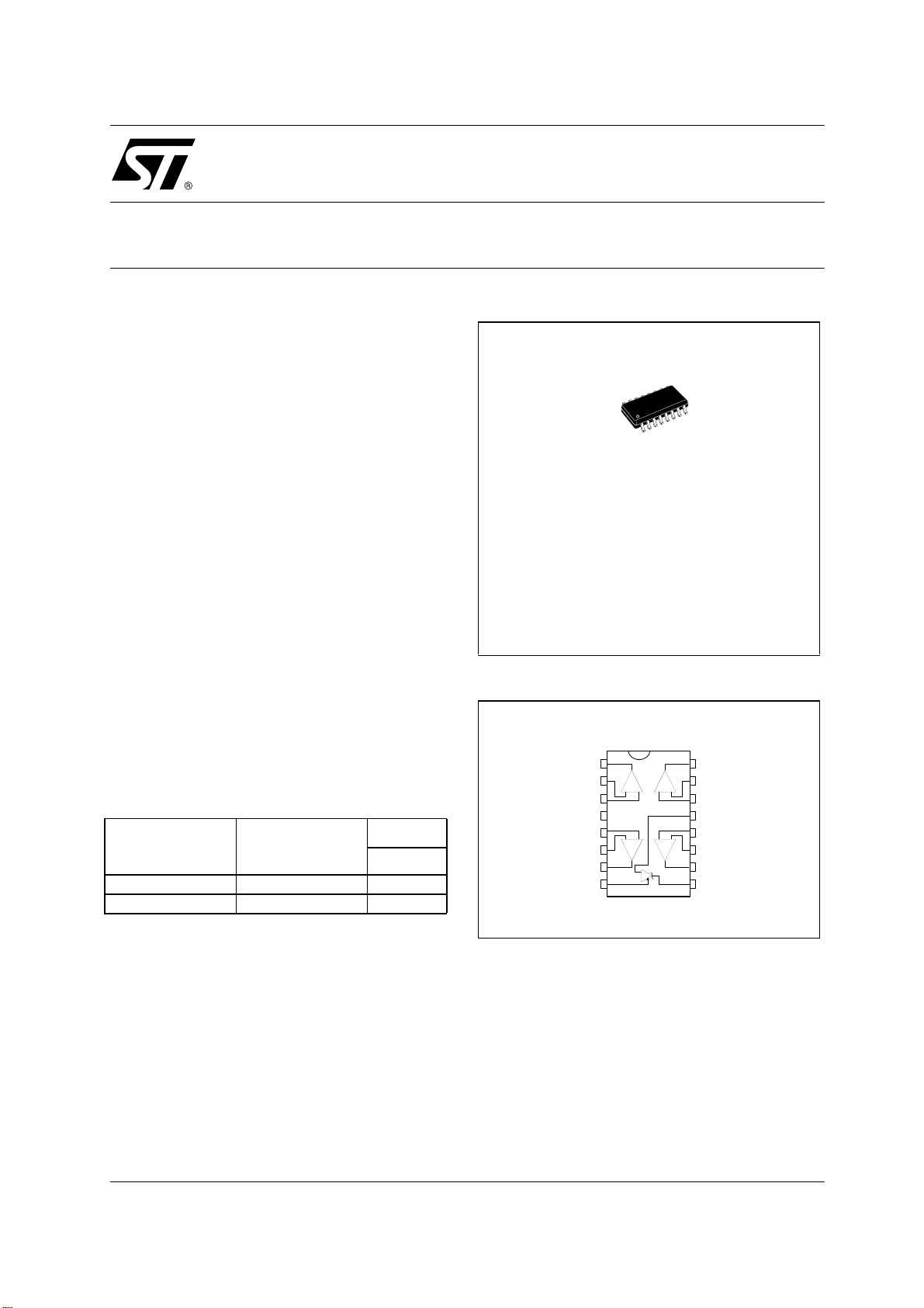
SO16
(Plastic Micropackage)
PIN CONNECTIONS (top view)
Output 1
Inverting Input 1
Non-inverting Input 1
V
CC
Non-inverting Input 2
Inverting Input 2
Output 2
Vref
1
2
3
COMP
+
4
5
6
7
8
COMP
16
15
14
13
12
11
10
9
Output 4
Inverting Input
Non-inverting Input 4
V
-
CC
Non-inverting Input 3
Inverting Input 3
Output 3
Cathode
January 2004
1/9
Page 2
TSM102/A
ABSOLUTE MAXIMUM RATINGS
Symbol Parameter Value Unit
V
T
ELECTRICAL CHARACTERISTICS
V
CC
Symbol Parameter Min. Typ Max. Unit
OPERATIONAL AMPLIFIER
V
CC
Symbol Parameter Min. Typ. Max. Unit
DV
A
SVR
V
CMR
V
V
DC supply Voltage 36 V
CC
V
Differential Input Voltage 36 V
id
V
Input Voltage -0.3 to +36 V
i
Operating Free-air Temperature Range -40 to +125 °C
oper
T
Maximum Junction Temperature 150 °C
j
Thermal Resistante Junction to Ambient 150 °C/W
+
= 5V, V
I
CC
+
= 5V, V
V
io
io
I
ib
I
io
-
= 0V, T
CC
Total Supply Current
T
≤ T
min.
= GND, R1 connected to V
CC
Input Offset Voltage
≤ T
T
min
= 25°C (unless otherwise specified)
amb
≤ T
amb
max
, T
= 25°C (unless otherwise specified)
amb
cc/2
≤ T
amb
max
0.8 1.5
14.5
Input Offset Voltage Drift 10 µV/°C
Input Bias Current
T
≤ T
min
amb
Input Offset Current
T
≤ T
min
amb
≤ T
≤ T
max
max
20 100
52040nA
Large Signal Voltage Gain
vd
R1=10k
≤ T
T
min
+
, V
= 30V, Vo = 5V to 25V
cc
≤ T
amb
max
50
25
100 V/mV
Supply Voltage Rejection Ratio
= 5V to 30V
V
cc
Input Common Mode Rejection Ratio
icm
≤ T
T
min
amb
≤ T
Common Mode Rejection Ratio
+
= 30V, Vicm = 0V to (V
V
cc
max
cc
+
) -1.8
(V
(V
80 100
-
cc
-
cc
) to (V
) to (V
cc
cc
+
) -1.8
+
) -2.2
70 90 dB
Output Short Circuit Current
V
= ±1V, Vo = 2.5V
I
sc
id
Source
Sink
3
3
6
6
High Level Output Voltage RL = 10kΩ
+
V
T
T
cc
min
min
= 30V
≤ T
amb
≤ T
amb
≤ T
≤ T
max
max
OH
Low Level Output Voltage RL = 10kΩ
OL
Slew Rate
V
SR
= ±15V
cc
= ±10V, RL = 10kΩ, CL = 100pF
V
i
27
28
26
100 150
1.6 2 V/
2
6.5
200
210
mA
mV
nA
dB
V
mA
V
mV
µs
2/9
Page 3
TSM102/A
Symbol Parameter Min. Typ. Max. Unit
GBP
∅m
Gain Bandwidth Product
= 10kΩ, CL = 100pF, f = 100kHZ
R
L
Phase Margin
= 10kΩ, CL = 100pF
R
L
1.4 2.1 MHz
Degrees
45
THD Toatal Harmonic Distortion 0.05 %
Equivalent Input Noise Voltage
e
n
f = 1kHz 29
COMPARATORS
+
= 5V, V
V
CC
Symbol Parameter Min. Typ Max. Unit
V
io
I
io
I
ib
I
OH
V
OL
A
vd
I
sink
V
icm
V
id
t
re
t
rel
1. The response time specified is for 100mV input step with 5mV overdrive.
For larger overdrive signals, 300ns can be obtained.
= Ground, T
CC
= 25°C (unless otherwise specified)
amb
Input Offset Voltage
T
≤ T
amb
≤ T
max
min
Input Offset Current
T
≤ T
amb
≤ T
max
min
Input Bias Current
T
≤ T
amb
≤ T
max
min
High Level Output Current
V
= 1V, Vcc = Vo = 30V
id
≤ T
T
min
amb
≤ T
max
Low Level Output Voltage
V
id
T
min
= -1V, I
≤ T
amb
sink
≤ T
= 4mA
max
Large Signal Voltage Gain
R1 = 15k, V
= 15V, Vo = 1 to 11V
cc
Output Sink Current
= -1V, Vo = 1.5V
V
id
Input Common Mode Voltage Range
T
≤ T
amb
≤ T
max
min
Differential Input Voltage
Response Time
R1 = 5.1k to V
1)
+
,V
= 1.4V
cc
ref
Large Signal Response Time
V
= 1.4V, Vi = TTL, R1 = 5.1k to V
ref
5
9
50
150
250
400
0.1
1
250 400
700
200
616 mA
+
V
0
0
-1.5
cc
+
-2
V
cc
+
V
cc
1.3 µs
+
cc
300
nV
----------- Hz
mV
nA
nA
nA
µA
mV
V/mV
V
V
ns
VOLTAGE REFERENCE
Symbol Parameter Value Unit
to 36
V
ref
3/9
V
Cathode to Anode Voltage
KA
I
Cathode Current 1 to 100 mA
k
V
Page 4

TSM102/A
V
ELECTRICAL CHARACTERISTICS
= 25°C (unless otherwise specified)
T
amb
Symbol Parameter Min. Typ Max. Unit
Reference Input Voltage -(figure1)- T
= V
KA
, IK = 10mA
ref
= V
ref
, IK = 10mA
V
ref
TSM102, V
KA
TSM102A, V
Reference Input Voltage Deviation Over
∆V
V
∆
---------------
∆
V
---------------V
∆
Tempera ture Range -(fig ure1, note1))
ref
ref
T∆
ref
KA
V
= V
KA
, IK = 10mA, T
ref
min
Temperature Coefficient of Reference Input Voltage - note
V
= V
KA
, IK = 10mA, T
ref
min
Ratio of Change in Reference Input Voltage to Change in Cathode to Anode Voltage -(figure2)
I
= 10mA, ∆V
K
= 36 to 3V
KA
Reference Input Current -(figure2)
I
= 10mA, R1 = 10kΩ, R2 = ∞
Iref
K
T
T
amb
min
= 25°C
≤ T
amb
≤ T
max
Reference Input Current Deviation Over
∆Iref
I
Temperature Range -(figure2)
I
= 10mA, R1 = 10kΩ, R2 = ∞
K
T
≤ T
= V
amb
ref
≤ T
max
min
Minimum Cathode Current for Regulation -(figure1)
min
V
KA
Ioff Off-State Cathode Current -(figure3) 180 500 nA
1. ∆V
2. The temperature coeffici ent is defined as the slopes (positive and negative) of the voltage vs temperature limits whithin
is defined as the difference between the maximum and minimum values obtained over the full temperature range.
ref
∆V
= Vref max. - Vref min
ref
which the reference voltage is guaranteed.
≤ T
≤ T
amb
amb
amb
= 25°C
≤ T
max
≤ T
max
2.475
2.490
2.500
2.500
2.525
2.510
730
2)
±22
±100
ppm/°C
-1.1 -2
1.5 2.5
3
0.5 1
0.5 1
V
mV
mV/V
µA
µA
mA
ref max.
V
ref min.
T1
T2
Temperature
max
2.5V
min
- n ppm / °C
+ n ppm / °C
25°C
Temperature
4/9
Page 5

TSM102/A
A
Figure 1 : Test Circuit for VKA = V
Input
Figure 2 : Test Circuit for V
Input
R
1
> V
KA
I
ref
ref
ref
V
ref
V
K
I
K
V
KA
I
K
V
KAVref
R1
1
------- -+
R2
I
ref
R1–+=
R
2
Figure 3 : Test Circuit for I
Input
off
V
ref
= 36V
V
KA
I
off
5/9
Page 6

e
APPLICATION NOTE
A BATTERY CHARGER USING THE TSM102
This application note explains how to use the
TSM102 in a n SMPS-type battery charger wh ich
features :
■ Voltage Control
■ Current Control
■ Low Battery Detection and End Of Charge
Detection
Figure 1: TSM 102 P inout
CC
1
2
3
+
5
6
7
TSM102
COMP
1 - TSM102 PRESENTATION
The TSM102 integrated circuit includes two Operational Amplifiers, two Comparators and one adjustable precision Voltage Reference (2.5V to
36V, 0.4% or 1%).
TSM102 can sustain up to 36V power supply voltage.
16
15
14
COMP
V
-
CC
12
11
10
Vref
2 - APPLICATION CONTEXT AND PRINCIPLE
OF OPERATION
In the battery charging field which requires ever increasing performances in more and more reduced
space, the TSM102A provides an attractive solution in terms of PCB area saving, precision and
versatility.
Figure 2 shows the secondary side of a battery
charger (SMPS type) where TSM 102A is used in
optimised conditions : the two Operational Amplifiers perform current a nd voltage control, the two
Comparators provide “End of Charge” and “Low
Battery” signals and the Voltage Reference ensures precise reference for all measurements.
The TSM102A is supplied by an auxiliary power
supply (forward configuration - D7) regulated by a
bipolar transistor and a zener diode on its base
(Q2 and DZ), and s mo othed by t he capac itors C3
Cathod
and C4. R15 polarizes the base of the transistor
and at the same time limits the current through the
zener diode during regulation mode of the auxiliary power supply.
The current and voltage regulations are made
thanks to the two Operational Amplifiers.
The first amplifier senses the current flow through
the sense resistor Rs and compares it with a part
of the reference voltage (resistor bridge R7, R8,
R9). The second amplifier compares the reference
voltage with a part of the charger’s outp ut (resistor
bridge R1, R2, R3).
When either of these two operational amplifiers
tends to lower its ouput, this linear information is
propagated towards the primary side via two OR ing diodes (D1, D2) and an optocoupler (D3). The
compensation loops o f these regulation functions
are ensured by the capacitors C1 and C2.
6/9
Page 7

TSM102/A
Figure 2 : T he Application Sc hem atic - Battery Charger Secondary Side
The first comparator ensures the “Low Battery”
signal generation thanks to the comparison of a
part of the charger’s output voltage (resistor
bridge R17, R19) and the reference voltage. Proper hysteresis is given thanks to R20. An improvement to the chargers security and to the b attery’s
life time optimization is achieved by lowering the
current control measurement thanks to Q1 that
shunts the resistor R9 when the battery’s voltage
is below the “Low Battery” level.
The second comparator ensures the “End of
Charge” signal generation thanks to the comparison of a part of the charger’s output voltage (resistor bridge R1, R2, R3) and the reference voltage.
When either of these two signals is acti ve, the corresponding LED is polarized for convenient visualization of the battery status.
3 - CALCULATION OF THE ELEMENTS
All the components values have been chosen for a
two-Lithium-Ion batteries charge application :
■ Current Control : 720mA (Low Battery current
control : 250mA)
■ Voltage Control : 8.4V (= 2x 4.2V)
■ Low Battery : 5.6V (= 2x 2.5V + 0.6V)
■ End of Charge : 8.3V (= 2x 4.15V)
Current Control :
The voltage reference is polarized than ks to the
R4 resistor (2.5mA), and the cathode of the reference gives a fixed 2.500V voltage.
I = U / R = [V
= [2.5 x (390 + 820) / (10000 + 390 + 820)] / 0.375
= 720mA
7/9
( R8 + R9 ) / (R7 + R8 + R9) ] / Rs
ref
I = 720mA
P = power dissipation through the sense resistor =
R I2 = 0.375 x 0.7202 = 194mW
In case of “Low Battery” conditions, the current
control is lowered thanks to the following
equation :
I = U / R = [ V
R8 / (R7 + R8 ) ] / Rs
ref
= [ 2.5 x 390 / (10000 + 390 ) ] / 0. 375
= 250mA
I (LoBatt) = 250mA
Voltage Control :
V
= V
out
/ [ R2 / (R1 + R2 + R3) ]
ref
= 2. 5 / [ 56 / (131.5 + 56 + 0.68 ) ]
= 8. 400V
V
= 8.400V
out
Low Battery signal :
If R5 = 0Ω and R6 = open :
V
(LoBatt) = Vref / [ R19 / ( R17 + R19 ) ]
out
= 2.5 / [ 10 / (12.4 + 10) ]
= 5.6V
V
(LoBatt) = 5.6 V
out
End of Charge signal :
V
(EOC) = Vref / [ (R2 + R3 ) / (R1 + R2 + R3) ]
out
= 2.5 / [(56 + 0.68) / (131.5 + 56 + 0.68)]
= 8.300V
V
(EOC)= 8.300V
out
Page 8

TSM102/A
Notes:
The current control values must be chosen in accordance with the elements of the primary side.
The performances of the battery charger in their
globality are highly d ependent on the adequation
of the primary and the secondary elements.
The addition of the diode D9 is necessary to avoid
dramatic discharge of the battery cells in case of
the charger disconnection from the mains voltage,
and therefore, the voltage measurement is to be
operated on the cathode side of the diode not to
take its voltage drop into account. The total bridge
value of R1, R2, R3 must ensure low battery discharge if the ch arger is disconnected from m ain,
but remains connected to the b attery by mistake.
Figure 3 : A precise power supply for the TSM102A and other components
The chosen values impose a 44µA discharge current max.
R12 and R13 are the equivalent resistors seen
from the opamp and from the comparator.
A hysteresis resistor can be connected to the “End
Of Charge” comparator to ensure prope r hysteresis to this signal, but this resistor must be chosen
carefully not to degrade the output voltage precision. It might be needed to impose unidirectionnal
hysteresis (by inserting a diode on the positive
feedback of the comparator).
Figure 3 shows how to use the integrated Voltage
Reference to build a precise Power Supply for the
TSM102A (and other components if necessary).
Pin 8 remains th e reference for all voltage measurements for the rest of the application.
aux
+
Vaux
9
8
Vcc
+
13
TSM102 Vref
8/9
Page 9

TSM102/A
PACKAGE MECHANICAL DATA
SO-16 MECHANICAL DATA
DIM.
A 1.75 0.068
a1 0.1 0.2 0.004 0.008
a2 1.65 0.064
b 0.35 0.46 0.013 0.018
b1 0.19 0.25 0.007 0.010
C 0.5 0.019
c1 45˚ (typ.)
D 9.8 10 0.385 0.393
E 5.8 6.2 0.228 0.244
e 1.27 0.050
e3 8.89 0.350
F 3.8 4.0 0.149 0.157
G 4.6 5.3 0.181 0.208
L 0.5 1.27 0.019 0.050
M 0.62 0.024
S8 ˚ (max.)
MIN. TYP MAX. MIN. TYP. MAX.
mm. inch
PO13H
Informat ion furnished is believed t o be accurate and reliable. H owever, STMicr oelectronics assumes no responsibility for the
consequences of use of such information nor for any infringement of patents or other rights of third parties which may result from
its use. No license is granted by implication or otherwise under any patent or pat ent rights of STMicroelectronics. Specifications
mentioned in this publication are subject to change without notice. This publicati on supersedes and replaces all information
previously supplied. STMicroe lectronics products are not au thorized for use as cr itical components in life s upport devices or
systems without express written approval of STMicroelectronics.
The ST logo is a registered trademark of STMicroelectronics
All other na mes are the pro p erty of thei r respecti ve o wners.
© 2004 STM i cr o electro n ic s - All Rights Reserve d
STMicroele ctronics GROUP OF C OM P ANIES
Australi a - B e l gium - Braz i l - Canada - Ch i na - Czech Rep ubi c - Finlan d - France - Germany
Hong Kong - India - Israel - Italy - J apan - Malaysia - Malta - Mo rocco - Sin gapore - Spai n
Sweden - Sw i tz e rland - Un i ted Kingdom - United Stat es
http://www.st.com
9/9
 Loading...