

Page 1
DUAL OPERATIONALAMPLIFIER - DUALCOMPARATOR
AND ADJUSTABLE VOLTAGE REFERENCE
OPERATIONALAMPLIFIERS
.
LOW SUPPLYCURRENT: 200µA/amp.
.
MEDIUMSPEED: 2.1MHz
.
LOW LEVEL OUTPUT VOLTAGECLOSE TO
-
V
: 0.1Vtyp.
CC
.
INPUTCOMMON MODE VOLTAGERANGE
INCLUDESGROUND
COMPARATORS
.
LOW SUPPLYCURRENT: 200µA/amp.
= 5V)
(V
CC
.
INPUTCOMMON MODE VOLTAGERANGE
INCLUDESGROUND
.
LOW OUTPUT SATURATIONVOLTAGE:
250mV (I
REFERENCE
.
ADJUSTABLEOUTPUT VOLTAGE :
V
ref
.
SINK CURRENTCAPABILITY :1 to 100mA
.
1%and 0.4%VOLTAGEPRECISION
.
LACTH-UP IMMUNITY
to 32V
= 4mA)
o
TSM102/A
N
DIP16
(Plastic Package)
D
SO16
(Plastic Micropackage)
ORDER CODES
Part number Temperature Range
o
TSM102I -40
TSM102AI -40
C, +85oC ••
o
C, +85oC ••
Package
ND
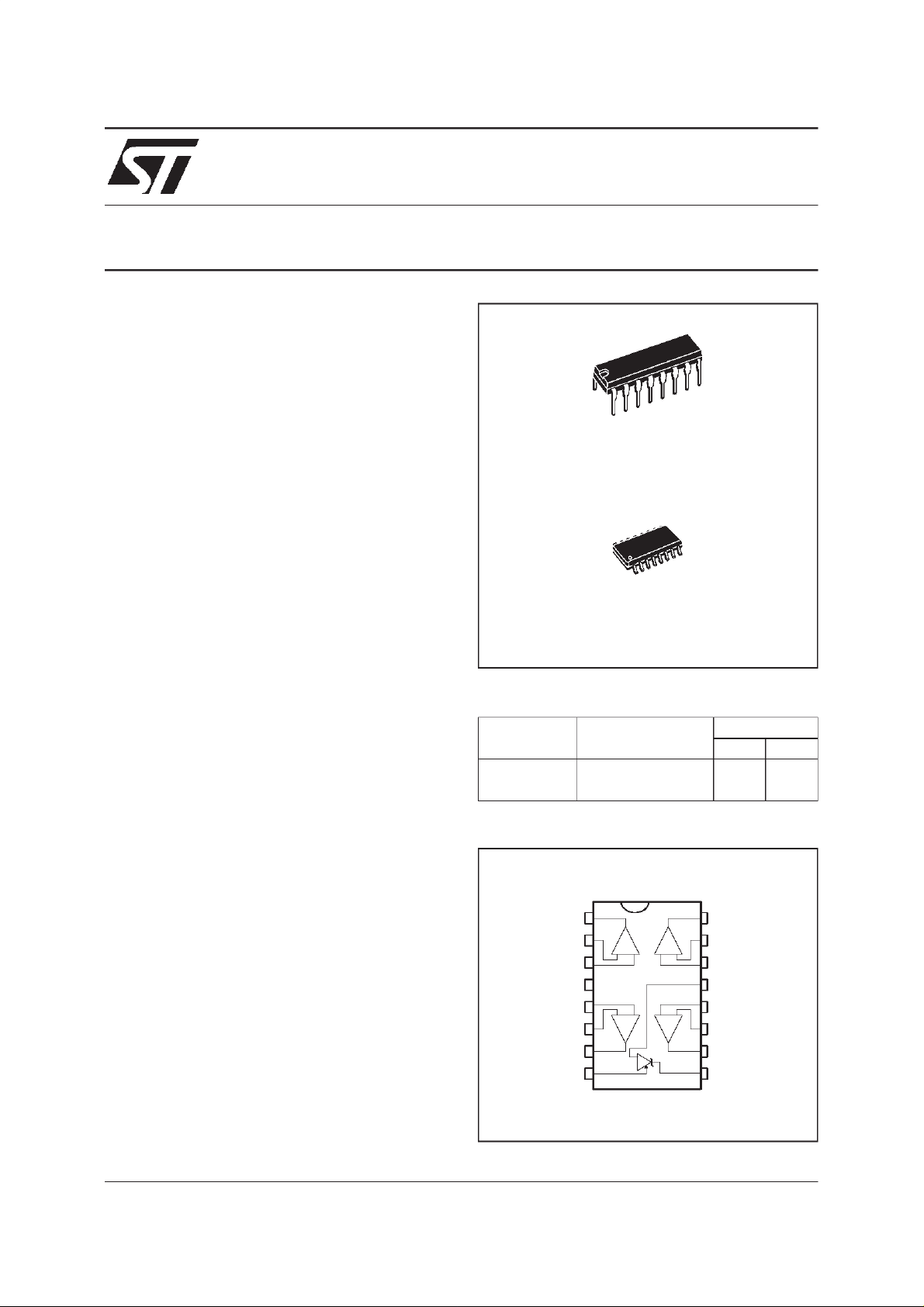
PIN CONNECTIONS
Output 1
1
Inverting Input 1
Non-inve rting Input 1
Non-inve rting Input 2
DESCRIPTION
The TSM102 is a monolithic IC that includes two
op-amps,twocomparatorsanda precisionvoltage
reference. This device is offering space and cost
savinginmanyapplicationslikepowersupplymanagement or data acquisitionsystems.
February1999 1/10
Inverting Input 2
V
Output 2
Vref
2
3
+
CC
COMP
4
5
6
7
8
COMP
16
Output 4
Inverting Input
15
Non-inverting Input 4
14
V
-
13
CC
Non-inverting Input 3
12
Inverting Input 3
11
10
Output 3
9
Ca thode
Page 2

TSM102
ABSOLUTE MAXIMUMRATINGS
Symbol Parameter Value Unit
V
CC
V
id
V
T
oper
T
ELECTRICAL CHARACTERISTICS
+
V
CC
Symbol Parameter Min Typ Max Unit
I
CC
OPERATIONALAMPLIFIERS
+
=5V,VCC=GND, R1 connectedto V
V
CC
Symbol Parameter Min. Typ. Max. Unit
V
io
DV
io
I
ib
I
io
A
vd
SVR Supply Voltage Rejection Ratio
V
icm
CMR CommonMode Rejection Ratio
I
sc
V
OH
V
OL
SR Slew Rate
GBP Gain BandwidthProduct
∅m Phase Margin
THD Total Harmonic Distortion
e
n
C
s
Supply Voltage 36 V
Differential Input Voltage 36 V
Input Voltage -0.3 to +36 V
i
Operating Free-air Temperature Range -40 to +125
Maximum Junction Temperature 150
j
Thermal Resistance Juction toAmbient (SO package) 150
=5V,V
-
=0V,T
CC
amb
Total Supply Current
T
min.<Tamb<Tmax.
Input Offset Voltage
≤ T
T
min.
amb
≤ T
=25oC (unlessotherwisespecified)
CC/2,Tamb
max.
=25oC (unlessotherwise specified)
0.8 1.5
2
1 4.5
6.5
Input Offset VoltageDrift 10 µV/oC
Input Bias Current
≤ T
T
min.
amb
≤ T
max.
Input Offset Current
≤ T
T
min.
Large Signal Voltage Gain
R1 = 10k, V
T
min.
V
CC
≤ T
amb
max.
+
= 30V, Vo= 5V to 25V
CC
≤ T
≤ T
amb
max.
= 5V to 30V 80 100
Input Common Mode VoltageRange
≤ T
T
min.
+
V
CC
amb
= 30V, V
≤ T
max.
icm
=0Vto(V
CC
+
) -1.8V
50
25
(VCC-)to(V
-
)to(V
(V
CC
70 90 dB
CC
CC
+
) -1.8
+
) -2.2
20 100
200
52040nA
100 V/mV
Output Short Circuit Current
= ±1V, Vo= 2.5V
V
id
Source
Sink
High Level Output Voltage RL= 10kΩ
+
= 30V
V
CC
≤ T
T
min.
amb
≤ T
max.
Low Level Output Voltage RL= 10kΩ
≤ T
T
min.
amb
≤ T
max.
27
26
3
3
6
6
28
100 150
210
1.6 2 V/µs
= ±15V
V
CC
= ±10V, RL= 10kΩ,CL= 100pF
V
i
1.4 2.1 MHz
= 10kΩ,CL= 100pF, f = 100kHz
R
L
= 10kΩ,CL= 100pF 45
R
L
0.05
Equivalent Input Noise Voltage
f = 1kHz 29
Channel Separation 120 dB
o
Degrees
o
C
o
C
C/W
mV
nA
dB
mA
mV
%
nV
√Hz
mA
V
V
2/10
Page 3

TSM102
COMPARATORS
+
=+5V,VCC=Ground, T
V
CC
Symbol Parameter Min. Typ. Max. Unit
V
I
I
I
OH
V
A
I
sink
V
V
t
t
Note 1 : The response time specified is for 100mV input step with 5mV overdrive.
Input Offset Voltage
io
Input Offset Current
io
Input Bias Current
ib
≤ T
≤ T
≤ T
amb
amb
amb
≤ T
≤ T
≤ T
T
min.
T
min.
T
min.
High Level Output Current
= 1V, VCC=Vo= 30V
V
id
≤ T
≤ T
amb
amb
sink
≤ T
≤ T
CC
T
min.
Low Level Output Voltage
OL
vd
= -1V, I
V
id
T
min.
Large Signal Voltage Gain
R1 = 15k, V
Output Sink Current
= -1V, Vo= 1.5V
V
id
Input Common Mode VoltageRange
icm
Differential Input Voltage V
id
Response Time - (note 1)
re
Large Signal Response Time
rel
For larger overdrive signals, 300ns can be obtained.
≤ T
T
min.
amb
≤ T
R1 = 5.1k to V
= 1.4V, Vi= TTL, R1 = 5.1k to V
V
ref
=25oC (unlessotherwise specified)
amb
max.
max.
max.
0.1
max.
= 4mA
max.
250 400
= 15V, Vo= 1 to 11V 200
616 mA
0
0
1.3 µs
300 ns
CC
max.
+
,V
ref
= 1.4V
CC
+
5
9
50
150
250
400
1
700
VCC+-1.5
+
-2
V
CC
+
CC
mV
nA
nA
nA
µA
mV
V/mV
V
V
3/10
Page 4

TSM102
VOLTAGEREFERENCE
Symbol Parameter Value Unit
V
KA
I
K
ELECTRICAL CHARACTERISTICS
=25oC (unless otherwise specified)
T
amb
Symbol Parameter Min. Typ. Max. Unit
V
ref
V
∆
ref
V
∆
ref
∆T
∆
V
ref
∆V
KA
Iref Reference InputCurrent - (figure 2)
I
∆
ref
I
min
I
off
Cathode to Anode Voltage V
to 36 V
ref
Cathode Current 1 to 100 mA
Reference InputVoltage - (figure 1) - T
TSM102, V
TSM102A, V
KA=Vref,IK
KA=Vref,IK
= 10mA
= 10mA
amb
=25oC
2.475
2.490
2.500
2.500
2.525
2.510
Reference InputVoltage Deviation Over
Temperature Range - (figure 1, note1)
V
KA=Vref,IK=
10mA, T
Temperature Coefficient of Reference Input Voltage - (note 2)
V
KA=Vref,IK
= 10mA, T
Ratio of Changein Reference Input Voltage to Changein Cathode to
min.
min.
≤ T
≤ T
amb
amb
≤ T
≤ T
max.
max.
730
ppm/
±22 ±100
mV/V
Anode Voltage - (figure 2)
= 10mA, ∆VKA= 36 to 3V -1.1 -2
I
K
= 10mA, R1= 10kΩ,R2=∞
I
K
T
T
amb
min.
=25oC
≤ T
amb
≤ T
max.
1.5 2.5
3
Reference InputCurrent Deviation Over
Temperature Range - (figure 2)
= 10mA, R1= 10kΩ,R2=∞
I
K
≤ T
T
min.
amb
≤ T
max.
0.5 1
Minimum Cathode Currentfor Regulation - (figure 1)
V
KA=Vref
0.5 1
Off-State Cathode Current - (figure 3) 180 500 nA
V
mV
µA
µA
mA
o
C
Notes : 1. ∆V
2. The temperature coefficientis defined asthe slopes (positive and negative) ofthe voltage vs temperature limits whithin
3. The dynamic Impedance is definedas |Z
is defined as the difference between themaximum and minimumvalues obtained over the full temperature
ref
range.
=V
∆V
ref max.-Vref min
ref
V
V
ref ma x.
ref m in.
T1
T2
Tempe rature
which thereference voltage isguaranteed.
-
n
p
p
m
/
C
C
/
m
p
p
n
ma x
2.5V
min
V
∆
KA
| =
KA
∆I
K
+
Temp era ture
25 C
4/10
Page 5

TSM102
Figure 1 : Test Circuitfor VKA=V
Input
Figure2 : Test Circuitfor VKA>V
Input
R
1
ref
ref
V
KA
I
K
V
ref
V
KA
I
K
I
ref
Figure 3 : Test Circuitfor I
Input
R
2
R
1
(1 +
)+I
ref
R
.R1
ref
2
off
V
ref
V
KA
I
off
VKA= V
= 36V
5/10
Page 6

TSM102
APPLICATION NOTE
A Li-Ion BATTERY CHARGER USING TSM102A
by R. LIOU
This application note explains how to use the
TSM102 in an SMPS-type battery charger which
features :
.
Voltage Control
.
CurrentControl
.
Low BatteryDetectionand End Of Charge
Detection
Figure 1 : TSM102Pinout
1
2
3
V
CC
Vref
COMP
+
5
6
7
1 - TSM102PRESENTATION
TheTSM102integratedcircuitincludestwoOperational Amplifiers,twoComparatorsandoneadjustable precision Voltage Reference (2.5V to 36V,
0.4% or 1%).
TSM102 can sustain upto 36Vpower supply volt-
age.
TSM102
COMP
16
15
14
V
-
CC
12
11
10
Ca thode
2 - APPLICATION CONTEXT AND PRINCIPLE
OF OPERATION
In the battery charging field which requires ever
increasing performances in more and more reduced space,the TSM102Aprovides an attractive
solutionintermsofPCB area saving,precisionand
versatility.
Figure 2 shows the secondary side of a battery
charger (SMPS type) where TSM102A is used in
optimisedconditions: the two OperationalAmplifiers perform current and voltage control, the two
Comparators provide ”End of Charge” and ”Low
Battery” signals and the Voltage Reference ensures precise reference for allmeasurements.
The TSM102A is supplied by an auxiliary power
supply (forward configuration- D7) regulated by a
bipolartransistorand a zenerdiode on itsbase(Q2
and DZ), and smoothedby the capacitorsC3 and
6/10
C4. R15polarizesthe baseof thetransistor andat
the same timelimits the currentthrough the zener
diodeduringregulationmodeoftheauxiliarypower
supply.
The current and voltage regulations are made
thanks to the two OperationalAmplifiers.
The first amplifier senses the current flowthrough
the sense resistor Rs and compares it with a part
of the reference voltage (resistor bridge R7, R8,
R9). The secondamplifiercomparesthe reference
voltagewith a part ofthe charger’s output(resistor
bridge R1, R2, R3).
When either of these two operational amplifiers
tends to lower its ouput, this linear information is
propagatedtowardstheprimarysideviatwoORing
diodes (D1, D2) and an optocoupler (D3). The
compensationloops of these regulation functions
are ensuredby the capacitorsC1 and C2.
Page 7

Figure2 : The ApplicationSchematic- Battery Charger SecondarySide
TSM102
The first comparator ensures the ”Low Battery”
signal generation thanks to the comparison of a
part ofthe charger’s output voltage (resistorbridge
R17, R19) and the referencevoltage. Proper hysteresis is given thanks to R20. An improvement to
the chargers security and to the battery’slife time
optimization is achieved by lowering the current
controlmeasurement thanksto Q1 that shuntsthe
resistor R9 when thebattery’svoltageis belowthe
”Low Battery” level.
The second comparator ensures the ”End of
Charge” signalgeneration thanks to the comparison ofa partof thecharger’s outputvoltage (resistor bridge R1,R2, R3) and the referencevoltage.
When either of these two signals is active, the
corresponding LED is polarized for convenient
visualizationof the battery status.
3 - CALCULATION OF THEELEMENTS
All thecomponentsvalueshavebeenchosenfor a
two-Lithium-Ionbatteries charge application:
.
CurrentControl : 720mA(Low Battery current
control : 250mA)
.
VoltageControl : 8.4V (=2x 4.2V)
.
LowBattery : 5.6V(= 2x 2.5V + 0.6V)
.
End of Charge : 8.3V(= 2x 4.15V)
Current Control :
Thevoltagereferenceispolarizedthanksto theR4
resistor (2.5mA), andthe cathode of the reference
gives a fixed2.500V voltage.
I = U / R = [ Vref ( R8 + R9 ) / (R7 + R8 + R9) ] / Rs
= [ 2.5 x (390 + 820) / (10000 + 390 + 820) ] / 0.375
= 720mA
I = 720mA
P = power dissipation through the sense resistor = R I2
= 0.375 x0.7202 = 194mW
In case of ”Low Battery” conditions, the current
controlis lowered thanks tothe following
equation:
I = U / R = = [ Vref R8 / (R7 + R8) ] / Rs
= [ 2.5 x 390/ (10000 + 390 ) ] / 0.375
= 250mA
I (LoBatt) = 250mA
Voltage Control :
Vout = Vref/ [ R2 / (R1 + R2 + R3) ]
7/10
Page 8

TSM102
= 2.5 / [ 56 / (131.5 + 56 + 0.68 ) ]
= 8.400V
Vout = 8.400V
Low Batterysignal :
IfR5 = 0Ωand R6 =open :
Vout(LoBatt) = Vref / [ R19 / ( R17 + R19 ) ]
= 2.5 / [ 10 / (12.4 + 10) ]
= 5.6V
Vout(LoBatt) = 5.6V
End of Charge signal:
Vout(EOC) = Vref / [ (R2 + R3 ) /(R1 + R2 + R3) ]
= 2.5 / [ (56 + 0.68) / (131.5 + 56 + 0.68) ]
= 8.300V
Vout(EOC)= 8.300V
Notes:
The current control values must be chosen in accordancewiththeelementsoftheprimaryside.The
performancesof the batterychargerin theirglobality are highly dependent on the adequationof the
primary and thesecondaryelements.
The additionof the diode D9 is necessary toavoid
dramatic discharge of the battery cells in case of
the chargerdisconnectionfrom themains voltage,
and therefore, the voltage measurement is to be
operated on the cathode side of the diode not to
take its voltage dropinto account.The total bridge
value of R1, R2, R3 must ensure low battery discharge if the charger is disconnected from main,
but remains connected to the battery by mistake.
The chosen valuesimpose a 44µAdischarge current max.
R12andR13 aretheequivalentresistorsseenfrom
the opampand from the comparator.
Ahysteresisresistorcan be connected to the ”End
Of Charge”comparatortoensureproperhysteresis
to this signal, but this resistor must be chosen
carefully not to degrade the output voltage precision.It might be neededto impose unidirectionnal
hysteresis (by inserting a diode on the positive
feedback of the comparator).
Figure 3 showshow to use the integratedVoltage
Referenceto build a precisePower Supplyfor the
Figure 3 : A precise power supply for theTSM102Aand othercomponents
Vaux
+
Vaux
9
8
13
TSM102 Vref
Vcc
+
8/10
Page 9

PACKAGE MECHANICAL DATA
16 PINS- PLASTICPACKAGE
TSM102
Dim.
a1 0.51 0.020
B 0.77 1.65 0.030 0.065
b 0.5 0.020
b1 0.25 0.010
D 20 0.787
E 8.5 0.335
e 2.54 0.100
e3 17.78 0.700
F 7.1 0.280
i 5.1 0.201
L 3.3 0.130
Z 1.27 0.050
Min. Typ. Max. Min. Typ. Max.
Millimeters Inches
9/10
Page 10

TSM102
PACKAGE MECHANICAL DATA
16 PINS- PLASTICMICROPACKAGE (SO)
Dim.
Min. Typ. Max. Min. Typ. Max.
Millimeters Inches
A 1.75 0.069
a1 0.1 0.2 0.004 0.008
a2 1.6 0.063
b 0.35 0.46 0.014 0.018
b1 0.19 0.25 0.007 0.010
C 0.5 0.020
c1 45
o
(typ.)
D 9.8 10 0.386 0.394
E 5.8 6.2 0.228 0.244
e 1.27 0.050
e3 8.89 0.350
F 3.8 4.0 0.150 0.157
G 4.6 5.3 0.181 0.209
L 0.5 1.27 0.020 0.050
M 0.62 0.024
S8
Information furnished is believed to be accurate and reliable. However, STMicroelectronics assumes no responsibility for the
consequences of use of such informationnor for any infringement of patents or other rights of third parties which may result from
its use. No license is granted by implication or otherwise under any patent or patent rights of STMicroelectronics. Specifications
mentioned in this publication are subject to change without notice. This publication supersedes and replaces all information
previously supplied.STMicroelectronics products arenot authorized foruseas critical componentsinlife support devicesorsystems
without express written approval of STMicroelectronics.
Australia - Brazil - Canada - China - France - Germany - Italy - Japan - Korea - Malaysia - Malta - Mexico - Morocco
The Netherlands- Singapore -Spain - Sweden -Switzerland -Taiwan - Thailand -United Kingdom -U.S.A.
The ST logo is a trademark of STMicroelectronics
1999 STMicroelectro nics–Printed in Italy– All RightsReserved
STMicroelectronicsGROUP OF COMPANIES
http://www.st.com
o
(max.)
10/10
 Loading...