

Page 1
Low Consumption Voltage and Current
Controller for Battery Chargers and Adaptors
■ Constant voltage and constant current
control
■ Low con sumpti on
■ Low voltage operation
■ Low external component count
■ Curre nt sink ou tput stage
■ Easy compensation
■ High ac mains voltage rejection
■ 2kV ESD protection (HBM)
Voltage Reference:
■ Fixed output voltage reference 1.25V
■ 0.5% and 1% Voltage precision
DESCRIPTION
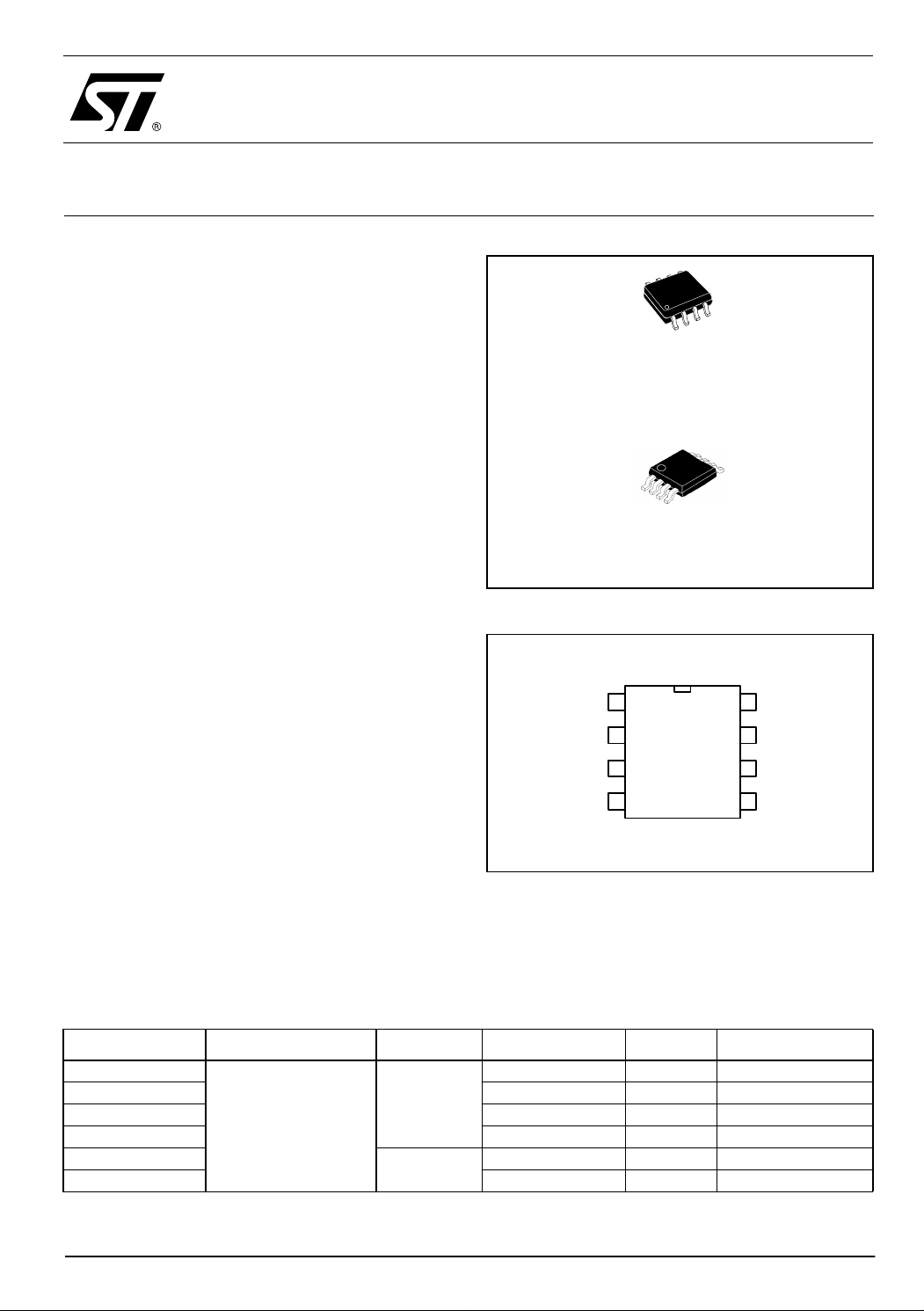
TSM1014
D
SO-8
(Plastic Package)
S
MiniSO-8
(Plastic Micropackage)
TSM1014 is a highly integrated solution for SMPS
PIN CONNECTIONS (top view)
applications requiring CV (cons tant voltage) and
CC (constant current) mode.
TSM1014 integrates one voltage reference and
1
VccVref
8
two operational amplifiers.
The voltage reference combined with one
operational amplifier makes it an ideal voltage
controller. The other operational amplifier,
combined with few external resistors and the
Cc-
3
Cc+
45
Cv- Cv Out
Cc Out 7
Gnd
6
2
voltage reference, can be used as a current
limiter.
APPLICATIONS
■ Adapters
■ Battery chargers
ORDER CODES
Part Number Temperature Range Package Packaging VRef (%) Marking
TSM1014ID
TSM1014IDT Tape & Reel 1 M1014
TSM1014AID Tube 0.5 M1014A
TSM1014AIDT Tape & Reel 0.5 M1014A
TSM1014IST
TSM1014AIST Tape & Reel 0.5 M809
-40 to 105°C
SO-8
mini SO-8
Tube 1 M1014
Tape & Reel 1 M808
July 2004 Revision 1 1/10
Page 2
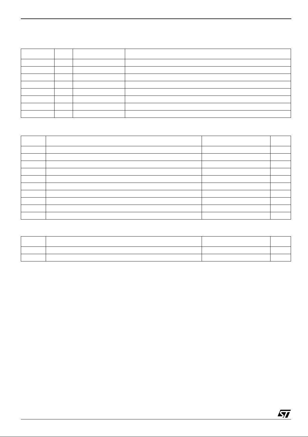
TSM1014 Pin Descriptions
1 Pin Descriptions
The table below gives the pin descriptions for both SO8 & MiniSO8 packages.
Name Pin # Type Function
VRef 1 Analog Output Voltage Reference
CC- 2 Analog Input Input pin of the operational amplifier
CC+ 3 Analog Input Input pin of the operational amplifier
CV- 4 Analog Input Input pin of the operational amplifier
CVOUT 5 Analog Output Output of the operational amplifier
Gnd 6 Power Supply Ground Line. 0V Reference For All Voltages
CCOUT 7 Analog Output Output of the operational amplifier
Vcc 8 Power Supply Power supply line.
2 Absolute Maximum Ratings
Symbol DC Supply Voltage Value Unit
Vcc DC Supply Voltage (50mA =< Icc) -0.3V to Vz V
Vi Input Voltage -0.3 to Vcc V
PT Power dissipation W
Toper Operational temperature 0 to 105 °C
Tstg Storage temperature -55 to 150 °C
Tj Junction temperature 150 °C
Iref Voltage reference output current 2.5 mA
ESD Electrostatic Discharge 2 kV
Rthja Thermal Resistance Junction to Ambient Mini SO8 package 180 °C/W
Rthja Thermal Resistance Junction to Ambient SO8 package 175 °C/W
3 Operating Cond itions
Symbol Parameter Value Unit
Vcc DC Supply Conditions 4.5 to Vz V
Toper Operational temperature -40 to 105 °C
2/10
Page 3
Electrical Characteristics TSM1014
4 Electrical Characteristics
Tamb = 25°C and Vcc = +18V (unless otherwise specified)
Symbol Parameter Test Condition Min Typ Max Unit
Total Current Consumption
Total Supply Current, excluding current
Icc
in Voltage Reference
1
.
Vz Vcc clamp voltage Icc = 50mA 28 V
Operator 1: Op-amp with non-inverting input connected to the internal VRef
Input Offset Voltage + Voltage reference
TSM1014
VRef+V
io
TSM1014A
Vcc = 18V, no load
Tmin. < Tamb < Tmax.
T
= 25°C
amb
T
≤ T
amb
= 25°C
≤ T
amb
≤ T
≤ T
max.
max.
min.
T
amb
T
min.
100 180 µA
1.251
1.25
1.266
1.279
1.258
1.267
V
DV
Input Offset Voltage Drift
io
7
µV/°C
Operator 2
Input Offset Voltage
V
io
DV
I
ib
SVR
TSM1014
TSM1014A
Input Offset Voltage Drift
io
Input Bias Current T
Supply Voltage Rejection Ration V
T
= 25°C
amb
T
≤ T
min.
T
T
T
amb
= 25°C
amb
≤ T
min.
amb
= 25°C
amb
≤ T
min.
amb
= 4.5V to 28V
CC
≤ T
≤ T
≤ T
max.
max.
max.
1
0.5
7
20
50
4
5
2
3
150
200
mV
µV/°C
nA
65 100 dB
Vicm Input Common Mode Voltage Range 0 Vcc-1.5 V
CMR
Common Mode Rejection Ratio T
T
amb
min.
= 25°C
≤ T
amb
≤ T
max.
70
60
85
dB
Output stage
Gm
Vol
Ios
Transconduction Gain. Sink Current
2
Only
Low output voltage at 5 mA sinking cur-
rent
Output Short Circuit Current. Output to
(Vcc-0.6V). Sink Current Only
T
T
T
T
T
amb
min.
min.
amb
min.
= 25°C
≤ T
amb
≤ T
amb
= 25°C
≤ T
amb
≤ T
≤ T
≤ T
max.
max.
max.
0.5
6
5
1
1
mA/mV
250 400 mV
10
mA
Voltage reference
Reference Input Voltage
TSM1014 1% precision
V
Ref
TSM1014A 0.5% precision
∆V
RegLine
RegLoad
1) Test conditions: pin 2 and 6 connected t o GND, pin 4 and 5 co nnected to 1.2 5V , pin 3 connected to 200mV.
2) The curr ent depends on the voltage dif f erence between the negati ve and the positive inputs of the amplifier. If the voltage on the minus
input is 1mV higher than the positive amplifier, the sinking current at the output OUT will be increased by Gm*1mA.
Reference Input Voltage Deviation Over
Ref
Temperature Range
Reference input voltage deviation over
Vcc range.
Reference input voltage deviation over
output current.
T
= 25°C
amb
T
≤ T
amb
= 25°C
≤ T
amb
≤ T
amb
≤ T
≤ T
≤ T
max.
max.
max.
min.
T
amb
T
min.
T
min.
Iload = 1mA
Vcc = 18V,
0 < Iload < 2.5mA
1.238
1.225
1.244
1.237
1.25
1.262
1.273
1.25
1.256
1.261
20 30 mV
20 mV
10 mV
V
3/10
Page 4

TSM1014 Electrical Characteristics
Figure 1: Internal schematic
Vref
1
Vref
Vcc
8
28V
Cc-
2
CC
Cc+
3
Cv- Cvout
45
CV
Ccout
Gnd
7
6
Figure 2: Typical adapter or battery charger application using TSM1014
DS
Vcc
CS
Rlimit
1
R4
100K
3
+
+
R5
Vsense
10K
Rsense
Vref
Cc+
IL
2
Ric2
1K
8
Vcc
28V
CV
TSM1014
CC
GndCc-
6
CV Out
Cv-
CC Out
Ric1
22K
R3
100
5
4
Rvc1
7
22K
Cic1
2.2nF
To primary
Cvc1
2.2nF
D
R2
R1
OUT+
IL
+
Load
OUT-
In the application schemat ic shown in Figure 2, the TSM1014 is used on the s econdary side of a f lyback
adapter (or battery charger) to provide an accurate voltage and current control. The above feedback loop
is made with optocoupler.
4/10
Page 5

Principles of Operation and A pplication Tips TSM1014
5 Principles of Operation and Application Tips
5.1 Voltage control
The voltage loop is controlled via a first trans-conductance operational amplifier, the resistor bridge R1,
R2, and the optocoupler which is directly connected to the output.
The relation between the values of R1 and R2 should be chosen as written in Equation 1.
R1 = R2 x V
Ref
/ (V
out
- V
) Equation 1
Ref
where V
is the desired output voltage.
out
To avoid the discharge of the load, the resistor bridge R1, R2 should be hi ghly resistive. For this type of
application, a total value of 100KΩ (or more) would be appropriate for the resistors R1 and R2.
As an example, with R2 = 100KΩ, V
= 4.10V, V
out
) = 1.210V, then R1 = 41.9KΩ.
Ref
Note that if the low drop diode is inserted between the load and the voltage regu lation resistor bridge to
avoid current flowing from the load through the resistor bridge, this drop should be taken into account in
the above calculations by replacing V
out
by (V
out
+ V
drop
).
5.2 Current control
The current loop is cont rolled via the second trans-conductance operational amplifier, the sense resist or
, and the optocoupler.
R
sense
V
threshold is achieved external ly by a resistor bridge tied to the V
sense
point is tied to the positive input of the current control operational amplifier, and its foot is to be connected
to lower potential point of the sense resistor as shown on the following figure. The resistors of this bridge
are matched to provide the best precision possible.
The control equation verifies:
R
× V
senseIlim
=
sense
voltage reference. Its middle
Ref
Equation 2
where I
Note that the R
is the desired limited current, and V
lim
resistor should be chosen taking into account the maximum dissipation (P
sense
through it during full load operation.
V
I
lim
sense
P
lim
R5V
⋅
-----------------------=
R5V
--------------------------------------- -=
sense
I
ref
R
+()
4R5
⋅⋅
refRsense
R
+()
4R5
is the threshold voltage for the current control loop.
×=
limVsense
Equation 3
lim
Equation 4
5/10
)
Page 6

TSM1014 Principles of Oper ation and Application Tips
Therefore, for most adapter and battery charger applications, a quarter-watt, or half-watt resistor to make
the current sensing function is sufficient.
The current sinking outputs of the two trans-conductance operational amplifiers are common (to the
output of the IC). This makes an ORing function which ensures that whenever the current or the voltage
reaches too high values, the optocoupler is activated.
The relation between the controlled current and the controlled output voltage can be described with a
square characteristic as shown in the following V/I output-power graph.
Figure 3: Output Voltage versus Output Current
Vout
Voltage regulat ion
TSM1014 Vcc : independent power supply
Secondary current r egulation
0
TSM1014 Vcc : On power out put
Primary cur rent regulation
Current regulation
Iout
5.3 Compensation
The voltage-control trans-conduc tance operational amplifier can be fully compensated. Both its output
and negative input are directly accessible for external compensation components.
An example of a suitable voltage-control compensation network is shown in Figure 2 on page 4. It
consists of a capacitor Cvc1=2.2n F and a resistor Rcv1 = 2 2KΩ in series.
The current-control trans-con ductan ce operat iona l ampli fier can be f ully compe nsated . Both of its out put
and negative input are directly accessible for external compensation components.
An example o f a suitable current-control c ompensation network is also shown in Figure 2 on p age 4. It
consists of a capacitor Cic1=2.2nF and a resistor Ric1=22KΩ in series .
5.4 Start-up and short circuit conditions
Under start-up or short-circuit conditions the TSM1014 is not provided with a high enough supply voltage.
This is due to the fact that the chip has its power supply line in common with the power supply line of the
system.
Therefore, the current limitation can only be ensured by the primary PWM module, which should be
chosen accordingly.
If the primary current limitation is considered not to be precise enough for the application, then a sufficient
supply for the TSM101 4 has to be ens ured under all co nditions. For this, it would be necessary to add
some circuitry to supply the chip with a separate power line. This can be achieved in a number of ways,
including putting an additional winding on the transformer.
6/10
Page 7

Principles of Operation and A pplication Tips TSM1014
5.5 Voltage clamp
The following schematic shows how to realize a low-cost power supply for the TSM1014 (with no
additional windings).Please pay a ttention to the fact that in the particular case presented here , this lowcost power supply can reach voltages as high as twice the voltage of the regulated line. Since the
Absolute Maximum Rating of the TSM1014 supply voltag e is 28V. In the aim to protect he TSM1014
against such how voltage values a internal zener clamp is integrated.
R
limit
V
ccVz
–()Ivz⋅=
Figure 4: Clamp voltage
Vcc
Rlimit
Vcc
Ivz
Vz
TSM1014
28V
Figure 5: Voltage controller and over current detection schematic
8
1
R4
100K
3
Cc+
+
R5
Vsense
10K
Rsense
IL
Vref
2
Ric2
1K
Vcc
CV
CC
28V
CV Out
Cv-
CC Out
GndCc-
6
CV
To primary
R3
1k
Rvc1
5
22K
4
7
Cvc1
2.2nF
Ric1
22K
OCP
R6
1K
Cic1
2.2nF
D
R2
R1
OUT+
IL
+
Load
OUT-
7/10
Page 8

TSM1014 Package Mechanical Data
6 Package Mechanical Data
SO-8 MECHANICAL DATA
DIM.
A 1.35 1.75 0.053 0.069
A1 0.10 0.25 0.04 0.010
A2 1.10 1.65 0.043 0.065
B 0.33 0.51 0.013 0.020
C 0.19 0.25 0.007 0.010
D 4.80 5.00 0.189 0.197
E 3.80 4.00 0.150 0.157
e 1.27 0.050
H 5.80 6.20 0.228 0.244
h 0.25 0.50 0.010 0.020
L 0.40 1.27 0.016 0.050
k ˚ (max.)
ddd 0.1 0.04
MIN. TYP MAX. MIN. TYP. MAX.
mm. inch
8
8/10
0016023/C
Page 9

Package Mechanical Data TSM1014
9/10
Page 10

TSM1014 Revision History
7 Revision History
Date Revision Description of Changes
01 July 2004 1 First Release
Information furnished is believed to be accurate and reliable. However, STMicroelectronics assumes no responsibility for the consequences
of use of such information nor for any infringement of patents or other rights of third parties which may result from its use. No license is granted
by implic ation or oth erwise unde r any patent or patent rights of S T M i c roelectron ics. Specifications me ntioned in this publication are subject
to change without notice. This publication supersedes and replaces all information previously supplied. STMicroelectronics products are not
authoriz ed for use as crit i cal components in life support devices or systems without expres s written approval of STMicroelect ronics.
The ST logo i s a registered trademark of STM i c roelectronics
All other nam es are the pro perty of their respective ow ners
© 2004 STMi croelectroni cs - All rights reserved
Austra l i a - B el gi u m - Brazil - Canada - China - Czech Repub i c - F i nland - Fran ce - Germany - Hong Kong - Indi a - Israel - Ital y - Japan -
Malaysia - M al ta - Morocco - Singapore - Sp ai n - Sweden - Swi tzerland - United Kingd om - United Sta tes of America
STMicroelectronics group of com panies
www.st.com
10/10
 Loading...