

Page 1
TSL253, TSL254
PRECISION HIGHSPEED LIGHTTOVOLTAGE CONVERTER
TAOS022 – JANUARY 2000
Monolithic Silicon IC Containing
Photodiode, Operational Amplifier, and
SR PACKAGE
(FRONT VIEW)
Feedback Components
Converts Light Intensity to Output Voltage
High Irradiance Responsivity...Typically
60 mV/(µW/cm2) at λp = 880 nm (TSL253)
321
High Bandwidth
Compact 3-Leaded Clear Plastic Package
Low Dark (Offset) Voltage . . . 10 mV Max
At 25°C, VDD = 5 V
Single-Supply Operation
Wide Supply-Voltage Range . . . 2.7 V to
5.5 V
Low Supply Current . . . 600 µA Typical at
VDD = 5 V
GND
Description
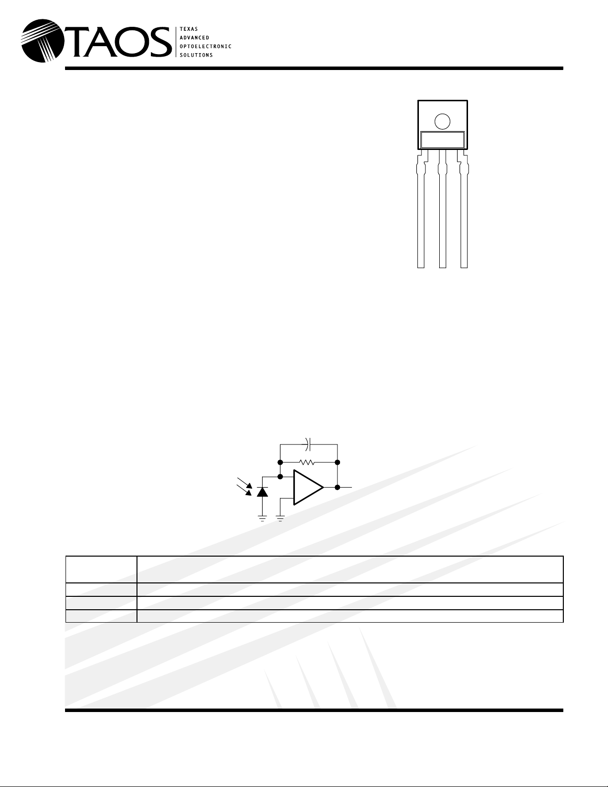
The TSL253 and TSL254 are light-to-voltage optical converters, each combining a 1-mm-square photodiode
and a transimpedance amplifier (feedback resistor = 16 MΩ, and 1 MΩ respectively) on a single monolithic IC.
Output voltage is directly proportional to the light intensity (irradiance) on the photodiode. These devices use
silicon-gate CMOS technology that provides improved amplifier offset-voltage stability and low power
consumption.
DD
OUTV
Functional Block Diagram
–
+
Terminal Functions
TERMINAL
NAME NO.
GND 1 Ground (substrate). All voltages are referenced to GND.
OUT 3 Output voltage
V
DD
www.taosinc.com
2 Supply voltage
Texas Advanced Optoelectronic Solutions Inc.
800 Jupiter Road, Suite 205 Plano, TX 75074 (972) 673-0759
Voltage
Output
DESCRIPTION
Copyright 2000, TAOS Inc.
1
Page 2
TSL253, TSL254
Tem erature coefficient of out ut
ngDD
µ √
PRECISION HIGHSPEED LIGHTTOVOLTAGE CONVERTER
TAOS022 – JANUARY 2000
Absolute Maximum Ratings over operating free-air temperature range (unless otherwise noted)
Supply voltage, VDD (see Note 1) 7 V. . . . . . . . . . . . . . . . . . . . . . . . . . . . . . . . . . . . . . . . . . . . . . . . . . . . . . . . . . . . .
Output current, IO ±10 mA. . . . . . . . . . . . . . . . . . . . . . . . . . . . . . . . . . . . . . . . . . . . . . . . . . . . . . . . . . . . . . . . . . . . . .
Duration of short-circuit current at (or below) 25°C 5 s. . . . . . . . . . . . . . . . . . . . . . . . . . . . . . . . . . . . . . . . . . . . . .
Operating free-air temperature range, TA –25°C to 85°C. . . . . . . . . . . . . . . . . . . . . . . . . . . . . . . . . . . . . . . . . . . .
Storage temperature range, T
–25°C to 85°C. . . . . . . . . . . . . . . . . . . . . . . . . . . . . . . . . . . . . . . . . . . . . . . . . . . .
stg
Lead temperature 1,6 mm (1/16 inch) from case for 10 seconds 240°C. . . . . . . . . . . . . . . . . . . . . . . . . . . . . . .
†
Stresses beyond those listed under “absolute maximum ratings” may cause permanent damage to the device. These are stress ratings only, and
functional operation of the device at these or any other conditions beyond those indicated under “recommended operating conditions” is not
implied. Exposure to absolute-maximum-rated conditions for extended periods may affect device reliability.
NOTE 1: All voltages are with respect to GND.
Recommended Operating Conditions
MIN MAX UNIT
Supply voltage, V
Operating free-air temperature, T
DD
A
2.7 5.5 V
0 70 °C
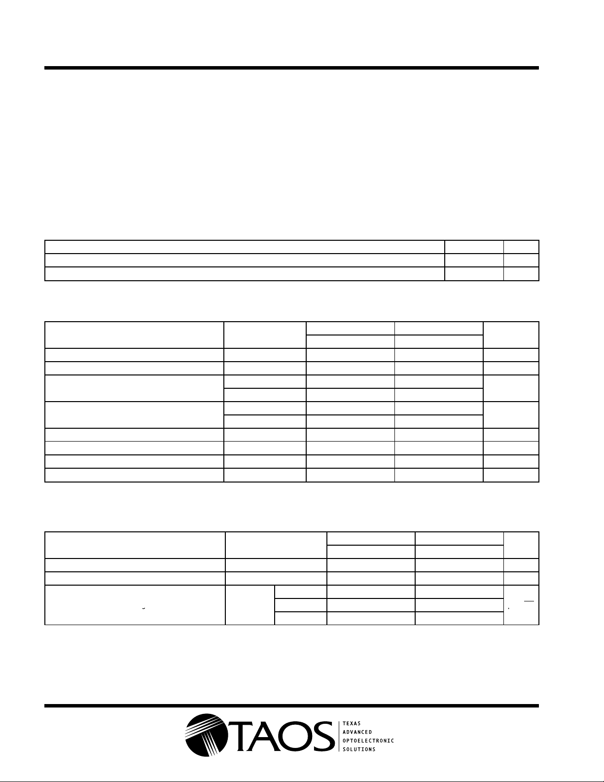
Electrical Characteristics at VDD = 5 V , TA = 25°C, λp = 880 nm, RL = 10 kΩ (unless otherwise noted)
(see Notes 2 and 3)
PARAMETER TEST CONDITIONS
VDDark voltage Ee = 0 10 10 mV
VOMMaximum output voltage swing Ee = 2 mW/cm
VOOutput voltage
Temperature coefficient of output
α
vo
voltage (VO)
NeIrradiance responsivity 60 3.5 mV/(µW/cm2)
Power supply rejection, dc 60 60 dB
Power supply rejection, ac fac = 1 kHz 18 44 dB
I
Supply current 0.6 1.5 0.6 1.5 mA
DD
NOTES: 2. The input irradiance Ee is supplied by a GaAlAs infrared-emitting diode with λp = 880 nm.
3. Irradiance responsivity is characterized over the range VO = 0.05 to 3 V.
Ee = 35 µW/cm
Ee = 595 µW/cm
300 nm < λ < 700 nm –0.2 –0.2
λp = 880 nm 0.05 0.05
2
2
2
TSL253 TSL254
MIN TYP MAX MIN TYP MAX
3 3.5 3 3.5 V
1.6 2 2.4
1.6 2 2.4
UNIT
V
%/°C
†
Switching Characteristics at TA = 25°C (see Figure 1)
PARAMETER TEST CONDITIONS
t
Output pulse rise time VDD = 5 V, λp = 880 nm 7.5 2 µs
r
t
Output pulse fall time VDD = 5 V, λp = 880 nm 7.5 2 µs
f
V
Output noise voltage VDD = 5 V f = 1 kHz 3 1 µV/√Hz
n
2
TSL253 TSL254
MIN TYP MAX MIN TYP MAX
f = 100 Hz 3 1.7
f = 10 kHz 6 1.3
www.taosinc.com
UNIT
Page 3
TSL253, TSL254
PRECISION HIGHSPEED LIGHTTOVOLTAGE CONVERTER
TAOS022 – JANUARY 2000
PARAMETER MEASUREMENT INFORMATION
V
DD
Pulse
Generator
IRED
(see Note A)
TSL25x
TEST CIRCUIT
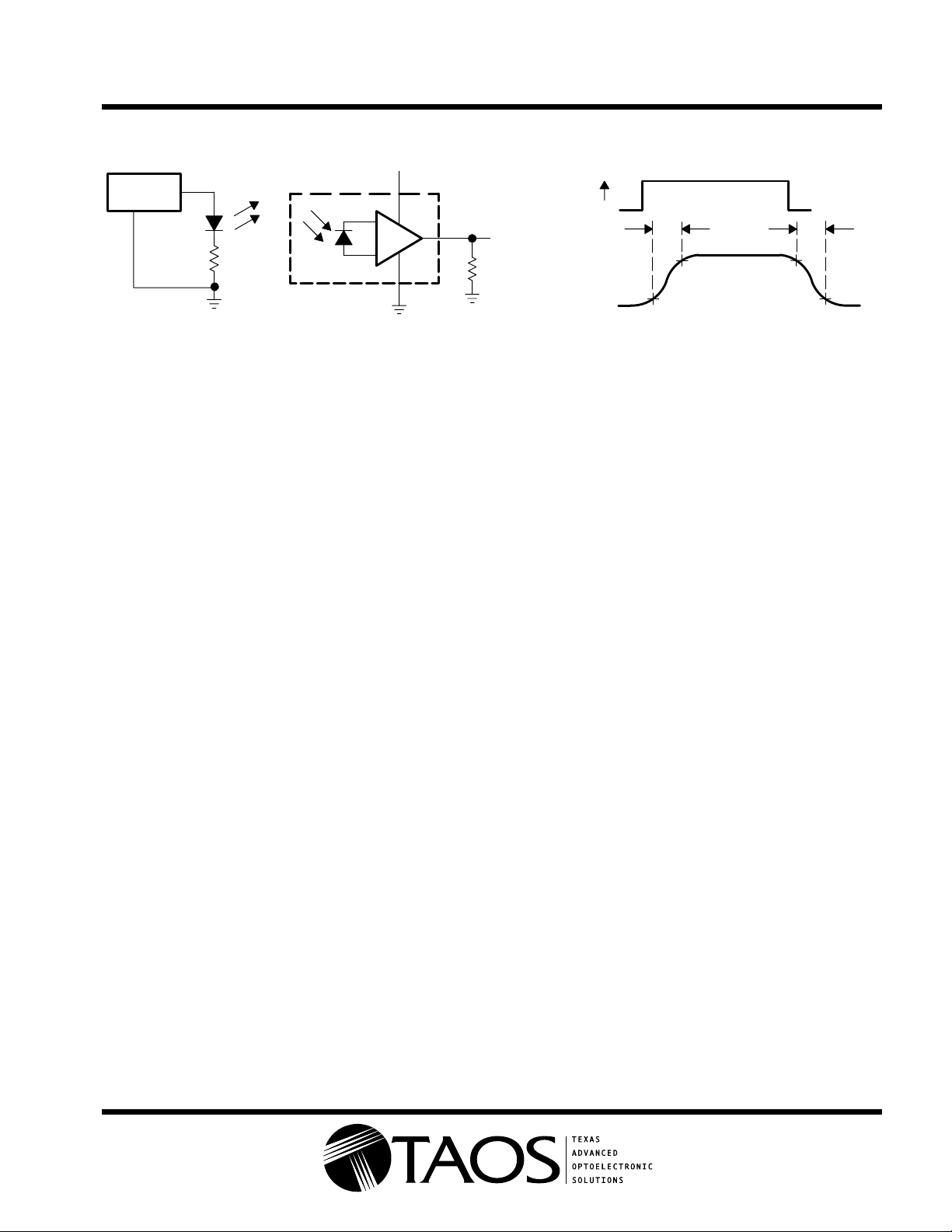
NOTES: A. The input irradiance is supplied by a pulsed GaAlAs infrared-emitting diode with the following characteristics: λp = 880 nm,
tr < 1 µs, tf < 1 µs.
B. The output waveform is monitored on an oscilloscope with the following characteristics: tr < 100 ns, Zi ≥ 1 MHz, Ci ≤ 20 pF.
2
–
+
3
1
R
Output
L
(see Note B)
Figure 1. Switching Times
Input
Output
E
e
t
r
90%
10%
VOLTAGE WAVEFORM
90%
10%
t
f
www.taosinc.com
3
Page 4
TSL253, TSL254
PRECISION HIGHSPEED LIGHTTOVOLTAGE CONVERTER
TAOS022 – JANUARY 2000
TYPICAL CHARACTERISTICS
OUTPUT VOLTAGE
10
1
0.1
– Output Voltage – V
O
V
0.01
VDD = 5 V
λp = 880 nm
No Load
TA = 25°C
vs
IRRADIANCE
TSL253
TSL254
Relative Responsivity
PHOTODIODE SPECTRAL RESPONSIVITY
1
TA = 25°C
0.8
0.6
0.4
0.2
0.001
1 10 100 1000
E
– Irradiance – µW/cm
e
2
Figure 2
MAXIMUM OUTPUT VOLTAGE
vs
SUPPLY VOLTAGE
5
2
– Maximum Output Voltage – V
V
OM
4
3
2
1
Ee = 2 mW/cm
λp = 880 nm
RL = 10 kΩ
TA = 25°C
0
300 500 700 900
λ – Wavelength – nm
Figure 3
NORMALIZED OUTPUT VOLTAGE
vs
ANGULAR DISPLACEMENT
1
0.8
0.6
0.4
Normalized Output Voltage
0.2
O
V –
Optical Axis
1100
0
3.5 4 4.5
VDD – Supply Voltage – V
53
Figure 4
4
0
80° 60° 40° 20° 0° 80°60°40°20°
θ – Angular Displacement
Figure 5
www.taosinc.com
Page 5
TSL253, TSL254
PRECISION HIGHSPEED LIGHTTOVOLTAGE CONVERTER
TAOS022 – JANUARY 2000
TYPICAL CHARACTERISTICS
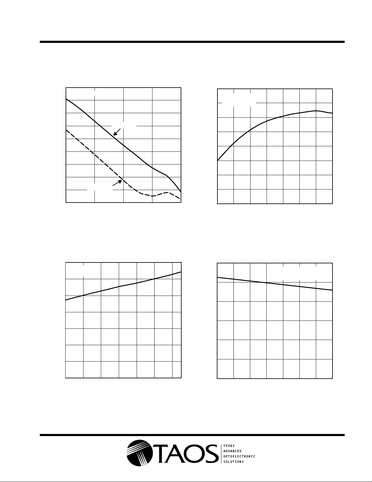
POWER SUPPLY REJECTION
FREQUENCY
70
TA = 25°C
60
50
40
30
20
10
Power Supply Rejection – dB
0
–10
–20
0.1 k
TSL253
1 k 10 k 100 k 1000 k
f – Frequency – Hz
Figure 6
SUPPLY CURRENT
SUPPLY VOLTAGE
0.7
TA = 25°C
No Load
0.6
vs
TSL254
vs
FREE-AIR TEMPERATURE
0.62
VDD = 5.5 V
0.61
0.60
0.59
0.58
0.57
– Supply Current – mA
DD
0.56
I
0.55
0.54
No Load
0
10 20 30 40
TA – Free-Air Temperature – °C
FREE-AIR TEMPERATURE
1.2
C
°
1
SUPPLY CURRENT
vs
50 60 70
Figure 7
OUTPUT VOLTAGE
vs
VDD = 5V
λp = 300 nm to 700 nm
0.5
0.4
0.3
– Supply Current – mA
0.2
DD
I
0.1
0
2.7 3.2 3.7 4.2 4.7
www.taosinc.com
VDD – Supply Voltage – V
Figure 8
5.2 5.7
0.8
0.6
0.4
0.2
– Output Voltage – Normelized to – 25
O
V
0
010203040
TA – Free-Air Temperature – °C
Figure 9
50 60 70
5
Page 6
TSL253, TSL254
PRECISION HIGHSPEED LIGHTTOVOLTAGE CONVERTER
TAOS022 – JANUARY 2000
TYPICAL CHARACTERISTICS
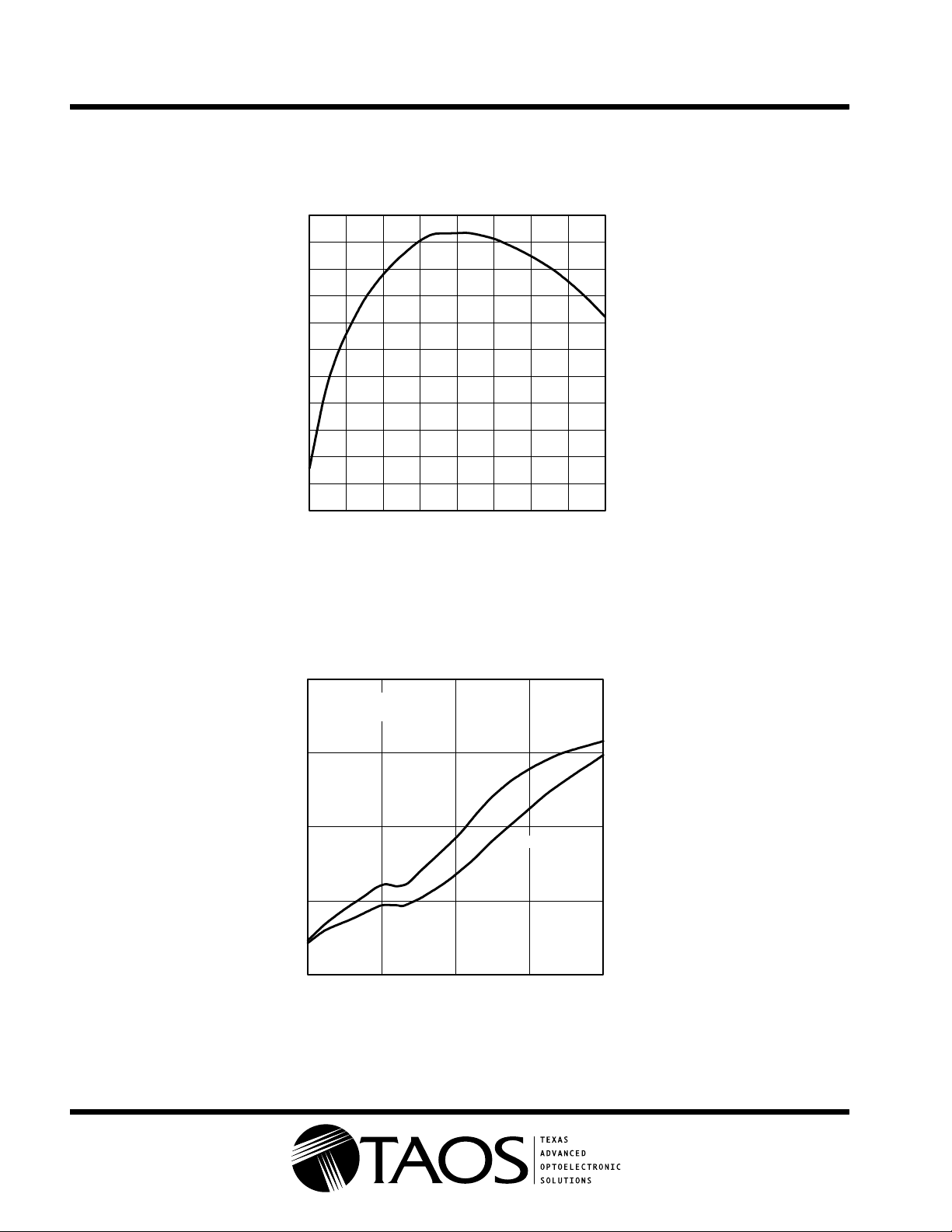
OUTPUT VOLTAGE
vs
SUPPLY VOLTAGE
1.001
1
0.999
0.998
0.997
0.996
0.995
0.994
0.993
0.992
– Output Voltage (Normalized) – V
O
V
0.991
0.99
2.5 3 3.5 4 4.5 5
VDD – Supply Voltage – V
5.5 6 6.5
Figure 10
INTEGRATED NOISE VOLTAGE
vs
MEASUREMENT BANDWIDTH FREQUENCY
5
10
VDD = 5 V
rms
Vµ
– Integrated Noise Voltage –
n
V
TA = 25°C
4
10
3
10
2
10
10
0.1 1 10
f – Measurement Bandwidth Frequency – kHz
TSL253
Figure 11
TSL254
100 1000
6
www.taosinc.com
Page 7
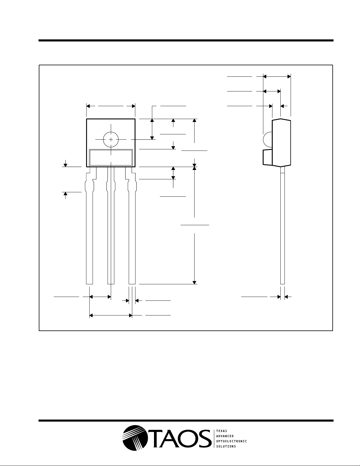
0.125 (3,18)
(See Note C)
PRECISION HIGHSPEED LIGHTTOVOLTAGE CONVERTER
MECHANICAL DATA
PLASTIC SINGLE-IN-LINE PACKAGE (OPTO)
0.191 (4,85)
0.171 (4,35)
0.081 (2,05)
0.061 (1,55)
0.120 (3,05)
0.100 (2,55)
0.189 (4,80)
0.173 (4,40)
0.049 (1,25)
0.029 (0,75)
TSL253, TSL254
TAOS022 – JANUARY 2000
0.108 (2,74)
0.092 (2,34)
0.069 (1,75)
0.049 (1,25)
0.033 (0,85)
0.014 (0,35)
21
0.084 (2,13)
0.074 (1,88)
NOTES: A. All linear dimensions are in inches (millimeters).
B. This drawing is subject to change without notice.
C. Lead dimensions are not controlled within this area.
D. All dimensions apply before solder dip.
E. Package body is a clear nonfilled optically transparent material
F. Index of refraction of clear plastic is 1.55.
3
0.025 (0,64)
0.016 (0,40)
0.165 (4,20)
0.150 (3,80)
0.619 (15,70)
0.520 (13,20)
0.020 (0,51)
0.015 (0,39)
www.taosinc.com
7
Page 8

TSL253, TSL254
PRECISION HIGHSPEED LIGHTTOVOLTAGE CONVERTER
TAOS022 – JANUARY 2000
PRODUCTION DATA — information in this document is current at publication date. Products conform to
specifications in accordance with the terms of Texas Advanced Optoelectronic Solutions, Inc. standard
warranty. Production processing does not necessarily include testing of all parameters.
NOTICE
Texas Advanced Optoelectronic Solutions, Inc. (T AOS) reserves the right to make changes to the products contained in this
document to improve performance or for any other purpose, or to discontinue them without notice. Customers are advised
to contact TAOS to obtain the latest product information before placing orders or designing TAOS products into systems.
TAOS assumes no responsibility for the use of any products or circuits described in this document or customer product
design, conveys no license, either expressed or implied, under any patent or other right, and makes no representation that
the circuits are free of patent infringement. TAOS further makes no claim as to the suitability of its products for any particular
purpose, nor does TAOS assume any liability arising out of the use of any product or circuit, and specifically disclaims any
and all liability, including without limitation consequential or incidental damages.
TEXAS ADVANCED OPTOELECTRONIC SOLUTIONS, INC. PRODUCTS ARE NOT DESIGNED OR INTENDED FOR
USE IN CRITICAL APPLICATIONS IN WHICH THE FAILURE OR MALFUNCTION OF THE TAOS PRODUCT MAY
RESUL T I N PERSONAL INJURY OR DE ATH. USE OF TAOS PRODUCTS IN LIFE SUPPORT SYSTEMS IS EXPRESSLY
UNAUTHORIZED AND ANY SUCH USE BY A CUSTOMER IS COMPLETELY AT THE CUSTOMER’S RISK.
8
www.taosinc.com
 Loading...