

Page 1
TSL230, TSL230A, TSL230B
PROGRAMMABLE LIGHTTOFREQUENCY CONVERTERS
TAOS004 – MAY 1999
High-Resolution Conversion of Light
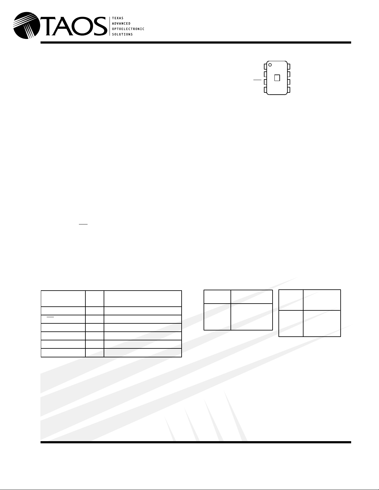
(TOP VIEW)
Intensity to Frequency With No External
Components
Programmable Sensitivity and Full-Scale
Output Frequency
Communicates Directly With a Microcontroller
GND
S0
S1
OE
8
S3
2
7
S2
3
6
OUT
4
5
V
DD
Single-Supply Operation Down to 2.7 V,
With Power-Down Feature
Absolute Output Frequency Tolerance of
±5% (TSL230B)
Nonlinearity Error Typically 0.2% at 100 kHz
Stable 100 ppm/°C Temperature Coefficient
Description
The TSL230, TSL230A, and TSL230B programmable light-to-frequency converters combine a configurable
silicon photodiode and a current-to-frequency converter on single monolithic CMOS integrated circuits. The
output can be either a pulse train or a square wave (50% duty cycle) with frequency directly proportional to light
intensity. Device sensitivity is selectable in three ranges, providing two decades of adjustment. The full-scale
output frequency can be scaled by one of four preset values. All inputs and the output are TTL compatible,
allowing direct two-way communication with a microcontroller for programming and output interface. An output
enable (OE) is provided that places the output in the high-impedance state for multiple-unit sharing of a
microcontroller input line. The devices are available with absolute-output-frequency tolerances of ±5%
(TSL230B), ±10% (TSL230A), or ±20% (TSL230). Each circuit has been temperature compensated for the
ultraviolet-to-visible-light range of 300 nm to 700 nm and are characterized for operation over the temperature
range of –25°C to 70°C.
Terminal Functions Selectable Options
TERMINAL
NAME NO.
GND 4 Ground
OE 3 I Enable for fO (active low)
OUT 6 O Scaled-frequency (fO) output
S0, S1 1, 2 I Sensitivity-select inputs
S2, S3 7, 8 I fO scaling-select inputs
V
DD
www.taosinc.com
I/O DESCRIPTION
5 Supply voltage
Texas Advanced Optoelectronic Solutions Inc.
800 Jupiter Road, Suite 205 Plano, TX 75074 (972) 673-0759
f
S1 S0 SENSITIVITY
L
H
L
H
Power Down
1×
10×
100×
L
L
H
H
S3 S2
L
L
L
H
H
L
H
H
Copyright 2001, TAOS Inc.
O
SCALING
(divide-by)
1
2
10
100
1
Page 2
TSL230, TSL230A, TSL230B
PROGRAMMABLE LIGHTTOFREQUENCY CONVERTERS
TAOS004 – MAY 1999
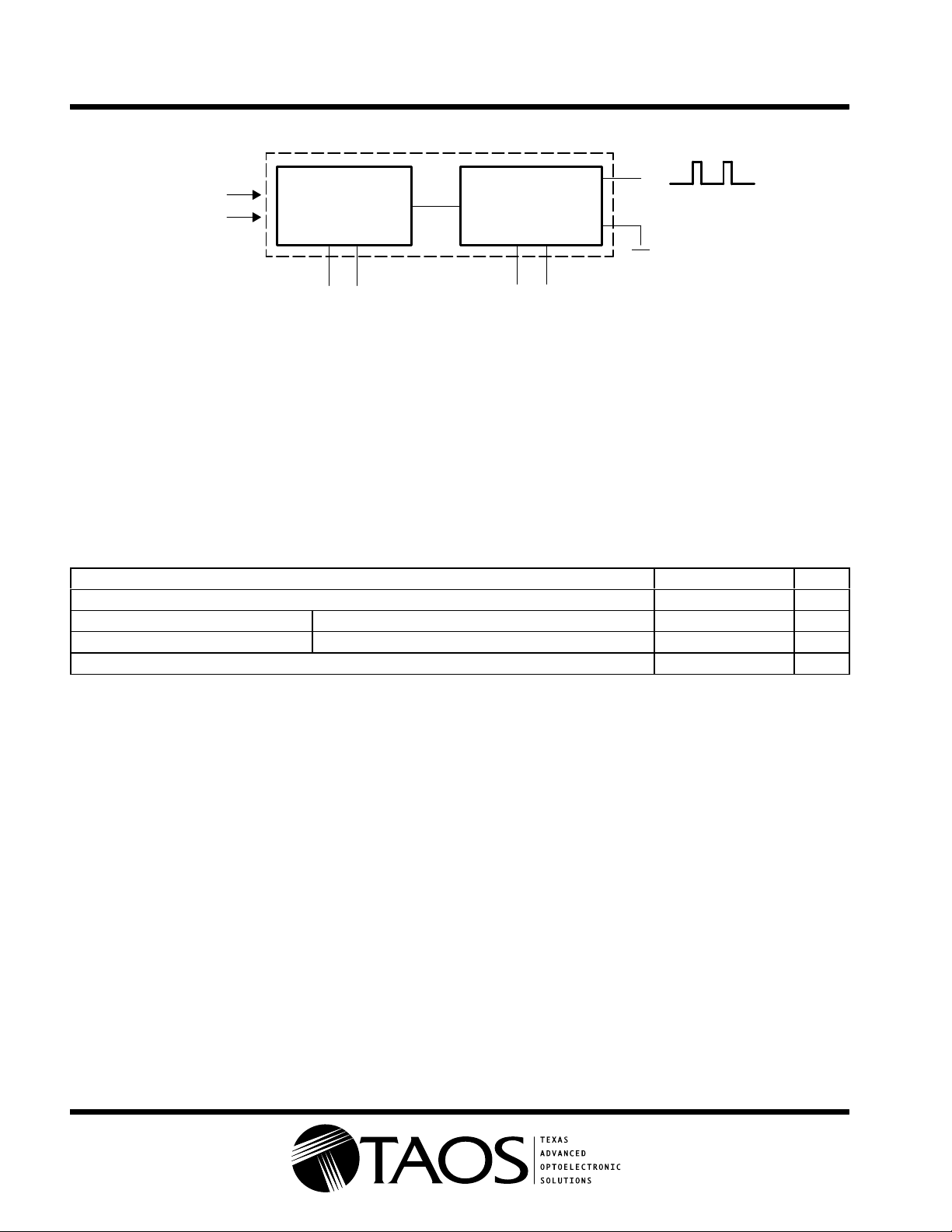
Functional Block Diagram
Output
Light
Photodiode
S0 S1 S2 S3
Current-to-Frequency
Converter
OE
Absolute Maximum Ratings over operating free-air temperature range (unless otherwise noted)
Supply voltage, VDD (see Note 1) 6.5 V. . . . . . . . . . . . . . . . . . . . . . . . . . . . . . . . . . . . . . . . . . . . . . . . . . . . . . . . . .
Input voltage range, all inputs, VI –0.3 V to VDD + 0.3 V. . . . . . . . . . . . . . . . . . . . . . . . . . . . . . . . . . . . . . . . . . . . .
Operating free-air temperature range, TA –25°C to 70°C. . . . . . . . . . . . . . . . . . . . . . . . . . . . . . . . . . . . . . . . . . . .
Storage temperature range –25°C to 85°C. . . . . . . . . . . . . . . . . . . . . . . . . . . . . . . . . . . . . . . . . . . . . . . . . . . . . . . .
Lead temperature 1,6 mm (1/16 inch) from case for 10 seconds 260°C. . . . . . . . . . . . . . . . . . . . . . . . . . . . . . .
†
Stresses beyond those listed under “absolute maximum ratings” may cause permanent damage to the device. These are stress ratings only , and
functional operation of the device at these or any other conditions beyond those indicated under “recommended operating conditions” is not
implied. Exposure to absolute-maximum-rated conditions for extended periods may affect device reliability.
NOTE 1: All voltage values are with respect to GND.
Recommended Operating Conditions
MIN NOM MAX UNIT
Supply voltage, V
High-level input voltage, V
Low-level input voltage, V
Operating free-air temperature range, T
DD
IH
IL
VDD = 4.5 V to 5.5 V 2 V
VDD = 4.5 V to 5.5 V 0 0.8 V
A
2.7 5 6 V
DD
–25 70 °C
V
†
Copyright 2001, TAOS Inc.
2
www.taosinc.com
Page 3
TSL230, TSL230A, TSL230B
Out ut ulse
Nonlinearity
PROGRAMMABLE LIGHTTOFREQUENCY CONVERTERS
TAOS004 – MAY 1999
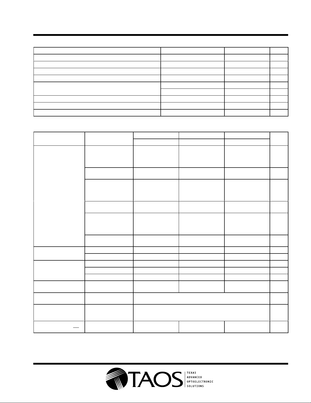
Electrical Characteristics at TA = 25°C, VDD = 5 V (unless otherwise noted)
PARAMETER TEST CONDITIONS MIN TYP MAX UNIT
V
OH
V
OL
I
IH
I
IL
I
DD
k
SVS
Operating Characteristics at VDD = 5 V, TA = 25°C
fOOutput frequency
t
w
†
Full-scale frequency is the maximum operating frequency of the device without saturation.
‡
Nonlinearity is defined as the deviation of fO from a straight line between zero and full scale, expressed as a percent of full scale.
§
Principal frequency is the internal oscillator frequency, equivalent to divide-by-1 output selection.
High-level output voltage IOH = –4 mA 4 4.3 V
Low-level output voltage IOL = 4 mA 0.17 0.26 V
High-level input current 1 µA
Low-level input current 1 µA
Supply current
Full-scale frequency
†
Power-on mode 2 3 mA
Power-down mode 10 µA
1.1 MHz
Temperature coefficient of output frequency λ ≤ 700 nm, –25°C ≤ TA ≤ 70°C ±100 ppm/°C
Supply voltage sensitivity VDD = 5 V ±10% 0.5 %/V
PARAMETER TEST CONDITIONS
TSL230 TSL230A TSL230B
MIN TYP MAX MIN TYP MAX MIN TYP MAX
S0 = H,
S1 = S2 = S3 = L,
Ee = 130 mW/cm2,
0.8 1 1.2 0.9 1 1.1 0.95 1 1.05 MHz
λp = 670 nm
Ee = 0, S0 = H,
S1 = S2 = S3 = L
0.1 10 0.1 10 0.1 10 Hz
S1 = H,
S0 = S2 = S3 = L,
Ee = 13 mW/cm2,
0.8 1 1.2 0.9 1 1.1 0.95 1 1.05 MHz
λp = 670 nm
Ee = 0 S1 = H,
S0 = S2 = S3 = L
0.13 10 0.13 10 0.13 10 Hz
S0 = S1 = H,
S2 = S3 = L,
Ee = 1.3 mW/cm2,
0.8 1 1.2 0.9 1 1.1 0.95 1 1.05 MHz
λp = 670 nm
Output pulse
duration
Nonlinearity
‡
Recovery from
power down
Step response to
full-scale step input
Response time to
programming
Ee = 0, S0 = S1 = H,
S2 = S3 = L
S2 = S3 = L 125 550 125 550 125 550 ns
S2 or S3 = H 1/2f
f
= 0 MHz to 10 kHz ±0.1% ±0.1% ±0.1% %F.S.
O
f
= 0 MHz to 100 kHz ±0.2% ±0.2% ±0.2% %F.S.
O
f
= 0 MHz to 1 MHz ±0.5% ±0.5% ±0.5% %F.S.
O
0.5 10 0.5 10 0.5 10 Hz
O
1/2f
O
1/2f
O
100 100 100 µs
1 pulse of new frequency plus 1 µs
2 periods of new principal frequency plus 1 µs
§
change
Response time to
output enable (OE)
50 150 50 150 50 150 ns
UNIT
s
www.taosinc.com
Copyright 2001, TAOS Inc.
3
Page 4
TSL230, TSL230A, TSL230B
PROGRAMMABLE LIGHTTOFREQUENCY CONVERTERS
TAOS004 – MAY 1999
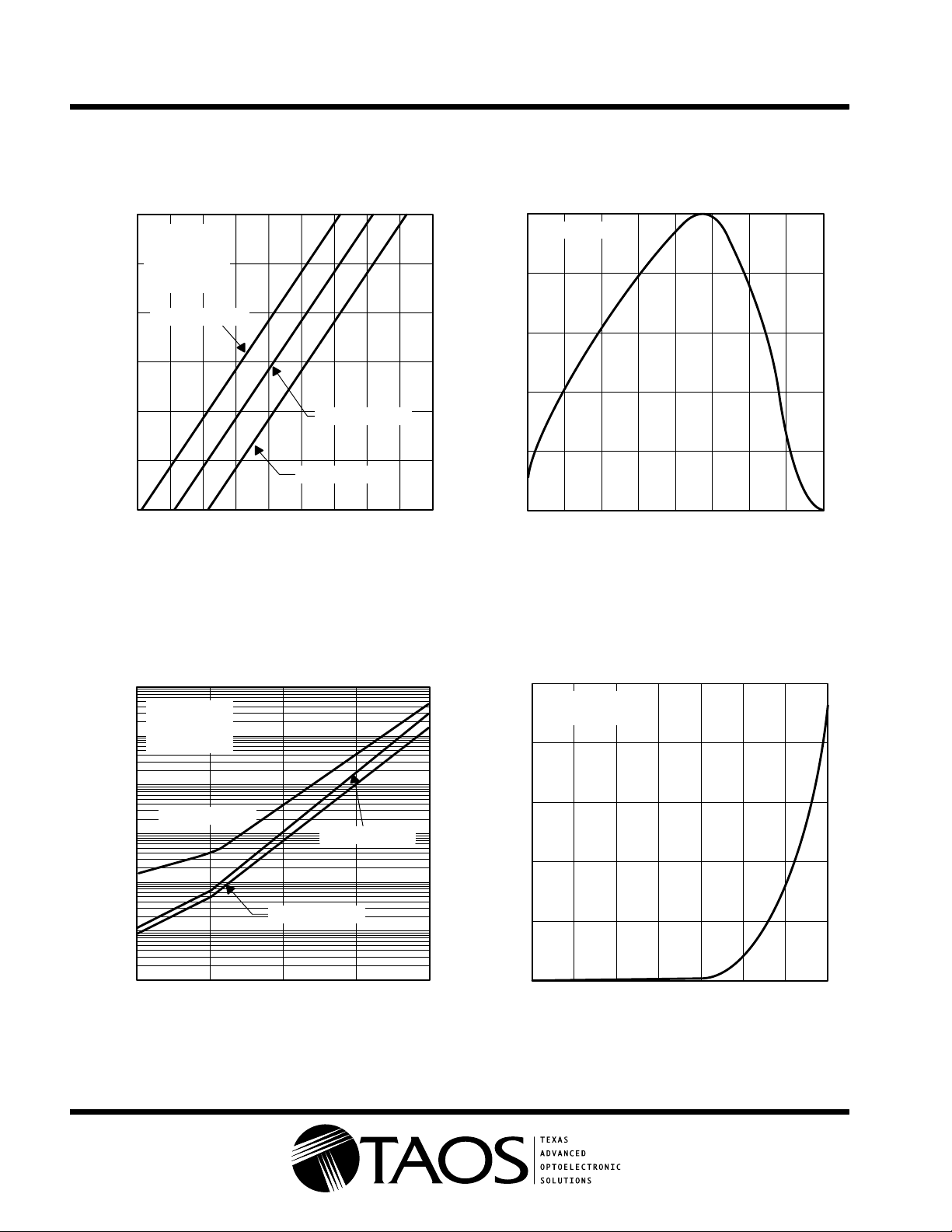
TYPICAL CHARACTERISTICS
OUTPUT FREQUENCY
vs
PHOTODIODE SPECTRAL RESPONSIVITY
1
TA = 25°C
0.8
0.6
0.4
0.2
1000
VDD = 5 V
λp = 670 nm
100
TA = 25°C
S2 = S3 = L
10
S0 = H, S1 = H
1
0.1
– Output Frequency – kHz
O
f
0.01
IRRADIANCE
S0 = L, S1 = H
Normalized Responsivity
S0 = H, S1 = L
0.001
0.001 0.01 0.1 1 10
100
VDD = 5 V
Ee = 0
10
S2 = S3 = L
1
S0 = H, S1 = H
0.1
– Dark Frequency – Hzf
0.01
O(dark)
0.001
100 1 k
Ee – Irradiance – µW/cm
10 k 100 k 1 M
2
0
300 500 700 900
λ – Wavelength – nm
Figure 1 Figure 2
TEMPERATURE COEFFICIENT
DARK FREQUENCY
vs
TEMPERATURE
S0 = L, S1 = H
S0 = H, S1 = L
C
°
10000
VDD = 5 V
TA = 25°C to 70°C
8000
6000
4000
2000
OF OUTPUT FREQUENCY
WAVELENGTH OF INCIDENT LIGHT
1100400 600 800 1000
vs
0.0001
– 25 0 25 50
Copyright 2001, TAOS Inc.
4
75
TA – Temperature – °C
0
Temperature Coefficient of Output Frequency – ppm/
300 500 700 900
400 600 800 1000
λ – Wavelength of Incident Light – nm
Figure 3 Figure 4
www.taosinc.com
Page 5
PROGRAMMABLE LIGHTTOFREQUENCY CONVERTERS
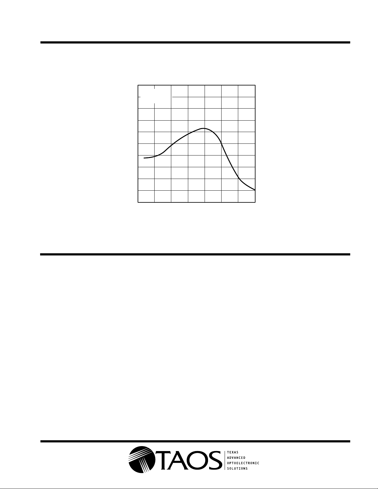
TYPICAL CHARACTERISTICS
OUTPUT FREQUENCY
SUPPLY VOLTAGE
1.005
1.004
1.003
1.002
1.001
0.999
0.998
Normalized Output Frequency
0.997
0.996
TA = 25°C
fO = 1 MHz
1
TSL230, TSL230A, TSL230B
TAOS004 – MAY 1999
vs
0.995
2.5 3 3.5 4 4.5
VDD – Supply Voltage – V
5 5.5
6
Figure 5
APPLICATION INFORMATION
Power-supply considerations
For optimum device performance, power-supply lines should be decoupled by a 0.01-µF to 0.1-µF capacitor
with short leads.
Output interface
The output of the device is designed to drive a standard TTL or CMOS logic input over short distances. If lines
greater than 12 inches are used on the output, a buffer or line driver is recommended.
Sensitivity adjustment
Sensitivity is controlled by two logic inputs, S0 and S1. Sensitivity is adjusted using an electronic iris technique
— effectively an aperture control — to change the response of the device to a given amount of light. The
sensitivity can be set to one of three levels: 1×, 10× or 100×, providing two decades of adjustment. This allows
the responsivity of the device to be optimized to a given light level while preserving the full-scale
output-frequency range. Changing of sensitivity also changes the effective photodiode area by the same factor .
www.taosinc.com
Copyright 2001, TAOS Inc.
5
Page 6

TSL230, TSL230A, TSL230B
PROGRAMMABLE LIGHTTOFREQUENCY CONVERTERS
TAOS004 – MAY 1999
APPLICATION INFORMATION
Output-frequency scaling
Output-frequency scaling is controlled by two logic inputs, S2 and S3. Scaling is accomplished on chip by
internally connecting the pulse-train output of the converter to a series of frequency dividers. Divided outputs
available are divide-by 2, 10, 100, and 1 (no division). Divided outputs are 50 percent-duty-cycle square waves
while the direct output (divide-by 1) is a fixed-pulse-width pulse train. Because division of the output frequency
is accomplished by counting pulses of the principal (divide-by 1) frequency, the final-output period represents
an average of n (where n is 2, 10, or 100) periods of the principal frequency. The output-scaling-counter registers
are cleared upon the next pulse of the principal frequency after any transition of the S0, S1, S2, S3, or OE lines.
The output goes high upon the next subsequent pulse of the principal frequency, beginning a new valid period.
This minimizes the time delay between a change on the input lines and the resulting new output period in the
divided output modes. In contrast with the sensitivity adjust, use of the divided outputs lowers both the full-scale
frequency and the dark frequency by the selected scale factor.
The frequency-scaling function allows the output range to be optimized for a variety of measurement
techniques. The divide-by-1 or straight-through output can be used with a frequency counter, pulse
accumulator, or high-speed timer (period measurement). The divided-down outputs may be used where only
a slower frequency counter is available, such as a low-cost microcontroller, or where period measurement
techniques are used. The divide-by-10 and divide-by-100 outputs provide lower frequency ranges for high
resolution-period measurement.
Measuring the frequency
The choice of interface and measurement technique depends on the desired resolution and data acquisition
rate. For maximum data-acquisition rate, period-measurement techniques are used.
Using the divide-by-2 output, data can be collected at a rate of twice the output frequency or one data point every
microsecond for full-scale output. Period measurement requires the use of a fast reference clock with available
resolution directly related to reference-clock rate. Output scaling can be used to increase the resolution for a
given clock rate or to maximize resolution as the light input changes. Period measurement is used to measure
rapidly varying light levels or to make a very fast measurement of a constant light source.
Maximum resolution and accuracy may be obtained using frequency-measurement, pulse-accumulation, or
integration techniques. Frequency measurements provide the added benefit of averaging out random- or
high-frequency variations (jitter) resulting from noise in the light signal. Resolution is limited mainly by available
counter registers and allowable measurement time. Frequency measurement is well suited for slowly varying
or constant light levels and for reading average light levels over short periods of time. Integration (the
accumulation of pulses over a very long period of time) can be used to measure exposure, the amount of light
present in an area over a given time period.
Copyright 2001, TAOS Inc.
6
www.taosinc.com
Page 7
TSL230, TSL230A, TSL230B
PROGRAMMABLE LIGHTTOFREQUENCY CONVERTERS
TAOS004 – MAY 1999
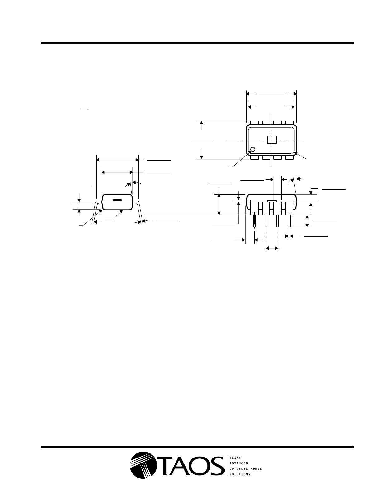
MECHANICAL INFORMATION
This dual-in-line package consists of an integrated circuit mounted on a lead frame and encapsulated with an
electrically nonconductive clear plastic compound. The photodiode area is typically 1.36 mm2 (0.0029 in2)
(S0 = S1 = H).
0.430 (10,92)
8 Places
0.410 (10,41)
0.390 (9,91)
‡
58
0.020 (0,51) R NOM
41
4 Places
(Center of active
area coincides
C
L
with package
center.)
8° MAX TYP
0.053 (1,35)
0.043 (1,09)
Pin 1 S0
Pin 2 S1
Pin 3 OE
Pin 4 GND
Pin 5 V
DD
Pin 6 OUT
Pin 7 S2
Pin 8 S3
0.075 (1,91)
0.060 (1,52)
0.310 (7,87)
0.290 (7,37)
0.260 (6,60)
0.240 (6,10)
10° TYP
0.310 (7,87)
0.290 (7,37)
0.030 (0,76) D NOM
0.175 (4,45)
0.155 (3,94)
0.060 (1,52)
0.040 (1,02)
105°
0.020 (0,51)
R MAX
4 Places
†
True position when unit is installed
‡
Minimum flat-optical-surface length
90°
8 Places
Seating Plane
0.012 (0,30)
0.008 (0,20)
0.016 (0,41)
0.014 (0,36)
0.067 (1,70)
0.053 (1,35)
NOTES: A. All linear dimensions are in inches and parenthetically in millimeters.
B. This drawing is subject to change without notice.
C. Index of refraction of clear plastic is 1.55.
0.025 (0,64)
0.015 (0,38)
0.100 (2,54) T.P.
0.150 (3,81)
0.125 (3,18)
†
www.taosinc.com
Copyright 2001, TAOS Inc.
7
Page 8

TSL230, TSL230A, TSL230B
PROGRAMMABLE LIGHTTOFREQUENCY CONVERTERS
TAOS004 – MAY 1999
PRODUCTION DATA — information in this document is current at publication date. Products conform to
specifications in accordance with the terms of Texas Advanced Optoelectronic Solutions, Inc. standard
warranty. Production processing does not necessarily include testing of all parameters.
NOTICE
Texas Advanced Optoelectronic Solutions, Inc. (TAOS) reserves the right to make changes to the products contained in this
document to improve performance or for any other purpose, or to discontinue them without notice. Customers are advised
to contact TAOS to obtain the latest product information before placing orders or designing TAOS products into systems.
TAOS assumes no responsibility for the use of any products or circuits described in this document or customer product
design, conveys no license, either expressed or implied, under any patent or other right, and makes no representation that
the circuits are free of patent infringement. TAOS further makes no claim as to the suitability of its products for any particular
purpose, nor does TAOS assume any liability arising out of the use of any product or circuit, and specifically disclaims any
and all liability, including without limitation consequential or incidental damages.
TEXAS ADVANCED OPTOELECTRONIC SOLUTIONS, INC. PRODUCTS ARE NOT DESIGNED OR INTENDED FOR
USE IN CRITICAL APPLICATIONS IN WHICH THE FAILURE OR MALFUNCTION OF THE TAOS PRODUCT MAY
RESUL T I N PERSONAL INJURY OR DEATH. USE OF T AOS PRODUCTS IN LIFE SUPPOR T SYSTEMS IS EXPRESSLY
UNAUTHORIZED AND ANY SUCH USE BY A CUSTOMER IS COMPLETELY AT THE CUSTOMER’S RISK.
TAOS, the TAOS logo, and Texas Advanced Optoelectronic Solutions are trademarks of Texas Advanced Optoelectronic Solutions
Incorporated.
Copyright 2001, TAOS Inc.
8
www.taosinc.com
 Loading...