

Page 1
TSL1402R
256 × 1 LINEAR SENSOR ARRAY WITH HOLD
TAOS041 – AUGUST 2002
256 × 1 Sensor-Element Organization
(TOP VIEW)
400 Dots-Per-Inch (DPI) Sensor Pitch
High Linearity and Uniformity
Wide Dynamic Range...4000:1 (72 dB)
Output Referenced to Ground
Low Image Lag ... 0.5% Typ
Operation to 8 MHz
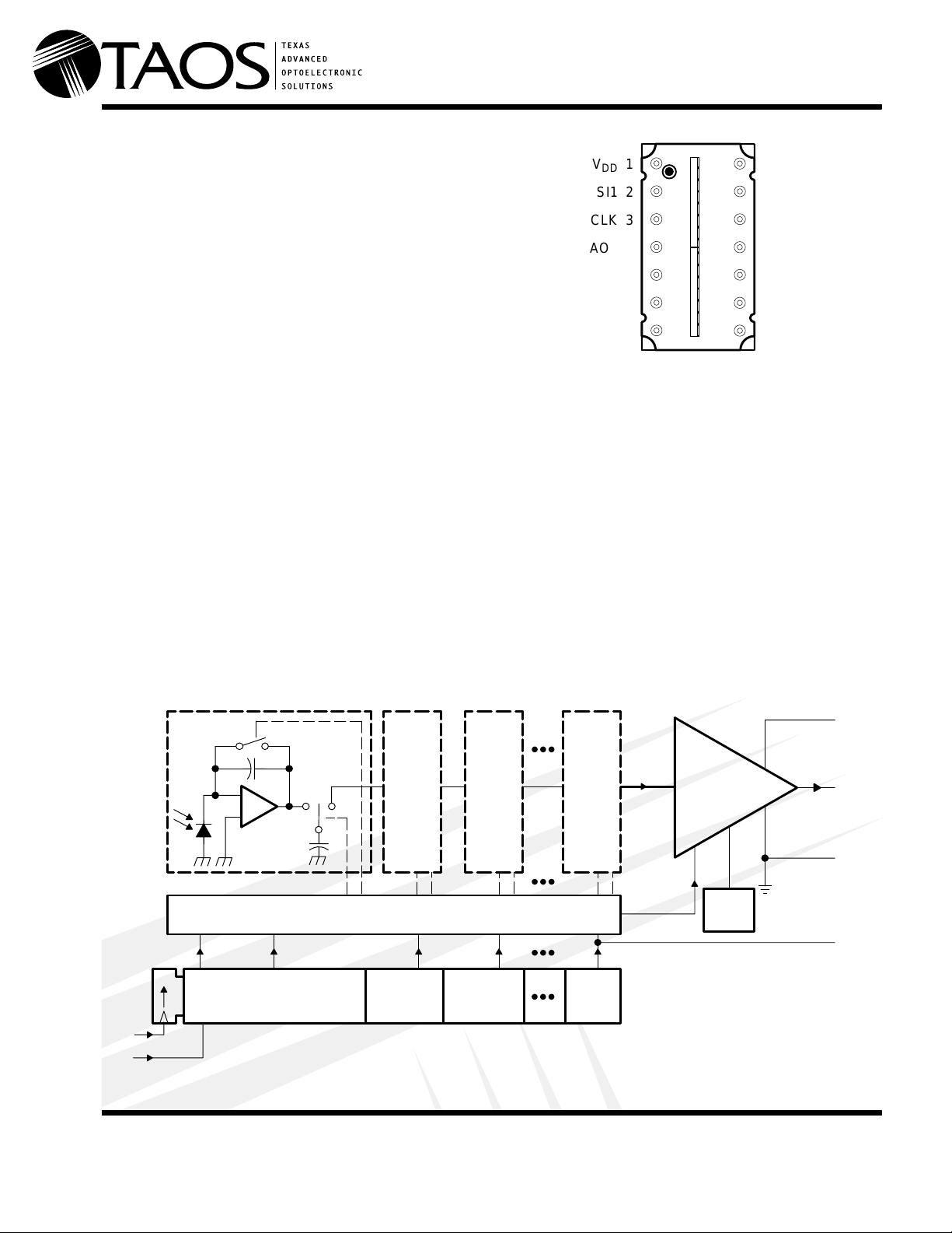
VDD 1
SI1 2
CLK 3
AO1 4
GND 5
14 NC
13 SO1
12 GND
11 NC
10 SI2
Single 3-V to 5-V Supply
Rail-to-Rail Output Swing (AO)
No External Load Resistor Required
Replacement for TSL1402
SO2 6
NC 7
NC – No internal connection
Description
The TSL1402R linear sensor array consists of two sections of 128 photodiodes each and associated charge
amplifier circuitry, aligned to form a contiguous 256 × 1 pixel array. The device incorporates a pixel data-hold
function that provides simultaneous integration start and stop times for all pixels. The pixels measure 63.5 µm
by 55.5 µm, with 63.5-µm center-to-center spacing and 8-µm spacing between pixels. Operation is simplified
by internal logic requiring only a serial-input pulse (SI) and a clock.
The TSL1402R is intended for use in a wide variety of applications including mark and code reading, OCR and
contact imaging, edge detection and positioning, and optical encoding.
9 NC
8 AO2
Functional Block Diagram (each section – pin numbers apply to section 1)
Pixel 1
_
+
Sample/Hold/
3
CLK 128-Bit Shift Register
2
SI
The
LUMENOLOGY
Company
Integrator
Reset
Output
Switch Control Logic
Pixel
2
Pixel
3
Q3Q2Q1Hold
Pixel
128
Analog
Bus
Q128
Texas Advanced Optoelectronic Solutions Inc.
800 Jupiter Road, Suite 205 Plano, TX 75074 (972) 673-0759
www.taosinc.com
Output
Buffer
Gain
Trim
Copyright 2002, TAOS Inc.
1
V
DD
4
AO
5
GND
13
SO
1
Page 2
TSL1402R
256 × 1 LINEAR SENSOR ARRAY WITH HOLD
TAOS041 – AUGUST 2002
Terminal Functions
TERMINAL
NAME NO.
AO1 4 Analog output of section 1.
AO2 8 Analog output of section 2.
CLK 3 Clock. Clk controls charge transfer, pixel output, and reset.
GND 5,12 Ground (substrate). All voltages are referenced to GND.
NC
SI1 2 Serial input (section 1). SI1 defines the start of the data-out sequence for section 1.
SI2 10 Serial input (section 2). SI2 defines the start of the data-out sequence for section 2.
SO1 13 Serial output (section 1). SO1 provides a signal to drive the SI2 input (in serial connection).
SO2 6
V
DD
7, 9,
11, 14
No internal connection.
Serial output (section 2). SO2 provides a signal to drive the SI input of another device for
cascading or as an end-of-data indication.
1 Supply voltage. Supply voltage for both analog and digital circuitry.
DESCRIPTION
Detailed Description
Device operation (assumes serial connection)
The sensor consists of 256 photodiodes, called pixels, arranged in a linear array. Light energy impinging on a
pixel generates photocurrent, which is then integrated by the active integration circuitry associated with that
pixel.
During the integration period, a sampling capacitor connects to the output of the integrator through an analog
switch. The amount of charge accumulated at each pixel is directly proportional to the light intensity on that pixel
and the integration time.
The output and reset of the integrators is controlled by a 256-bit shift register and reset logic. An output cycle
is initiated by clocking in a logic 1 on SI1. An internal signal, called Hold, is generated from the rising edge of
SI1 and simultaneously transmitted to sections 1 and 2. This causes all 256 sampling capacitors to be
disconnected from their respective integrators and starts an integrator reset period. As the SI pulse is clocked
through the shift register, the charge stored on the sampling capacitors is sequentially connected to a
charge-coupled output amplifier that generates a voltage on analog output AO. Simultaneously, during the first
18 clock cycles, all pixel integrators are reset, and the next integration cycle begins on the 19th clock. On the
128th clock rising edge, the SI pulse is clocked out on the SO1 pin (section 1) and becomes the SI pulse for
section 2 (SI2). The rising edge of the 129th clock cycle terminates the SO1 pulse, and returns the analog output
AO1 of section 1 to high-impedance state. Analog output AO2 now becomes the active output. As in section
2, SO2 is clocked out on the 256th clock pulse. Note that a 257th clock pulse is needed to terminate the SO2
pulse and return AO2 to the high-impedance state.
Copyright 2002, TAOS Inc.
2
www.taosinc.com
The
LUMENOLOGY
Company
Page 3

TSL1402R
256 × 1 LINEAR SENSOR ARRAY WITH HOLD
TAOS041 – AUGUST 2002
AO is an op amp-type output that does not require an external pull-down resistor. This design allows a rail-to-rail
output voltage swing. With V
for saturation light level.
The voltage developed at analog output (AO) is given by:
where:
V
out
V
drk
R
E
e
t
int
is the analog output voltage for white condition
is the analog output voltage for dark condition
is the device responsivity for a given wavelength of light given in V/(µJ/cm2)
e
is the incident irradiance in µW/cm
is integration time in seconds
When the device is not in the output phase, AO is in a high-impedance state.
The TSL1402R can be connected in the serial mode, where it takes 256 clocks to read out all pixels, or in the
parallel mode where it takes 128 clocks to read out all pixels (see
9 and 10).
A 0.1 µF bypass capacitor should be connected between VDD and ground as close as possible to the device.
= 5 V, the output is nominally 0 V for no light input, 2 V for normal white level, and 4.8 V
DD
V
= V
out
+ (Re) (Ee)(t
drk
2
int
)
APPLICATION INFORMATION
and FIgures
The
LUMENOLOGY
Company
www.taosinc.com
Copyright 2002, TAOS Inc.
3
Page 4
TSL1402R
256 × 1 LINEAR SENSOR ARRAY WITH HOLD
TAOS041 – AUGUST 2002
Absolute Maximum Ratings
†
Supply voltage range, VDD –0.3 V to 6 V. . . . . . . . . . . . . . . . . . . . . . . . . . . . . . . . . . . . . . . . . . . . . . . . . . . . . . . . . . .
Input voltage range, VI –0.3 V to VDD + 0.3V. . . . . . . . . . . . . . . . . . . . . . . . . . . . . . . . . . . . . . . . . . . . . . . . . . . . . . .
Input clamp current, IIK (VI < 0) or (VI > VDD) –20 mA to 20 mA. . . . . . . . . . . . . . . . . . . . . . . . . . . . . . . . . . . . . . .
Output clamp current, IOK (VO < 0 or VO > VDD) –25 mA to 25 mA. . . . . . . . . . . . . . . . . . . . . . . . . . . . . . . . . . . .
Voltage range applied to any output in the high impedance or power-off state, VO –0.3 V to VDD + 0.3 V. . .
Continuous output current, I
(V
= 0 to VDD) –25 mA to 25 mA. . . . . . . . . . . . . . . . . . . . . . . . . . . . . . . . . . . . . .
O
O
Continuous current through VDD or GND –40 mA to 40 mA. . . . . . . . . . . . . . . . . . . . . . . . . . . . . . . . . . . . . . . . . .
Analog output current range, IO –25 mA to 25 mA. . . . . . . . . . . . . . . . . . . . . . . . . . . . . . . . . . . . . . . . . . . . . . . . . .
Maximum light exposure at 638 nm 5 mJ/cm
. . . . . . . . . . . . . . . . . . . . . . . . . . . . . . . . . . . . . . . . . . . . . . . . . . . . . .
Operating free-air temperature range, TA 0°C to 70°C. . . . . . . . . . . . . . . . . . . . . . . . . . . . . . . . . . . . . . . . . . . . . .
Storage temperature range, T
–25°C to 85°C. . . . . . . . . . . . . . . . . . . . . . . . . . . . . . . . . . . . . . . . . . . . . . . . . . . .
stg
Lead temperature 1,6 mm (1/16 inch) from case for 10 seconds 260°C. . . . . . . . . . . . . . . . . . . . . . . . . . . . . . .
†
Stresses beyond those listed under “Absolute Maximum Ratings” may cause permanent damage to the device. These are stress ratings only, and
functional operation of the device at these or any other conditions beyond those indicated under “Recommended Operating Conditions” is not
implied. Exposure to absolute-maximum-rated conditions for extended periods may affect device reliability.
Recommended Operating Conditions (see Figure 1 and Figure 2)
MIN NOM MAX UNIT
Supply voltage, V
Input voltage, V
High-level input voltage, V
Low-level input voltage, V
Wavelength of light source, λ 400 1000 nm
Clock frequency, f
Sensor integration time, Parallel, t
Sensor integration time, Serial, t
Setup time, serial input, t
Hold time, serial input, t
Operating free-air temperature, T
NOTE 1: SI must go low before the rising edge of the next clock pulse.
DD
I
IH
IL
clock
int
int
su(SI)
(see Note 1) 0 ns
h(SI)
A
3 5 5.5 V
0 V
2 V
0 0.8 V
5 8000 kHz
0.018 100 ms
0.034 100 ms
20 ns
0 70 °C
DD
DD
V
V
2
Copyright 2002, TAOS Inc.
4
www.taosinc.com
The
LUMENOLOGY
Company
Page 5

TSL1402R
256 × 1 LINEAR SENSOR ARRAY WITH HOLD
TAOS041 – AUGUST 2002
Electrical Characteristics at f
= 330 Ω, Ee = 11 µW/cm2 (unless otherwise noted) (see Note 2)
R
L
= 1 MHz, VDD = 5 V, TA = 25°C, λp = 640 nm, t
clock
= 5 ms,
int
PARAMETER TEST CONDITIONS MIN TYP MAX UNIT
V
V
Analog output voltage (white, average over 256 pixels) See Note 3 1.6 2 2.4 V
out
Analog output voltage (dark, average over 256 pixels) Ee = 0 0 0.1 0.2 V
drk
PRNU Pixel response nonuniformity See Note 4 ±10%
Nonlinearity of analog output voltage See Note 5 ±0.4%
Output noise voltage See Note 6 1 mVrms
R
V
SE Saturation exposure
DSNU Dark signal nonuniformity All pixels, E
Responsivity See Note 7 25 35 45
e
V
= 5 V, RL = 330 Ω 4.5 4.8
Analog output saturation voltage
sat
DD
V
= 3 V, RL = 330 Ω 2.5 2.8
DD
V
= 5 V, See Note 8 136
DD
V
= 3 V, See Note 8 78
DD
= 0, See Note 9 0.04 0.12 V
e
IL Image lag See Note 10 0.5%
V
= 5 V, E
I
I
I
C
C
DD
IH
IL
Supply current
High-level input current VI = V
Low-level input current VI = 0 10 µA
Input capacitance, SI 5 pF
i
Input capacitance, CLK 10 pF
i
V
DD
DD
= 3 V, E
= 0 6 9
e
= 0 5 8
e
DD
NOTES: 2. All measurements made with a 0.1 µF capacitor connected between VDD and ground.
3. The array is uniformly illuminated with a diffused LED source having a peak wavelength of 640 nm.
4. PRNU is the maximum difference between the voltage from any single pixel and the average output voltage from all pixels of the
device under test when the array is uniformly illuminated at the white irradiance level. PRNU includes DSNU.
5. Nonlinearity is defined as the maximum deviation from a best-fit straight line over the dark-to-white irradiance levels, as a percent
of analog output voltage (white).
6. RMS noise is the standard deviation of a single-pixel output under constant illumination as observed over a 5-second period.
7. R
8. SE(min) = [V
e(min)
= [V
out(min)
sat(min)
– V
– V
drk(max)
drk(min)
] ÷ (Ee × t
] ×〈Ee × t
int
)
int
) ÷[V
out(max)
– V
drk(min)
]
9. DSNU is the difference between the maximum and minimum output voltage for all pixels in the absence of illumination.
10. Image lag is a residual signal left in a pixel from a previous exposure. It is defined as a percent of white-level signal remaining after
a pixel is exposed to a white condition followed by a dark condition:
IL
V
V
out (white)
out (IL)
V
V
drk
100
drk
V/
(µJ/cm2)
nJ/cm
mA
10 µA
V
2
Timing Requirements (see Figure 1 and Figure 2)
t
t
t
tr, t
NOTES: 11. Input pulses have the following characteristics: tr = 6 ns, tf = 6 ns.
The
Setup time, serial input (see Note 11) 20 ns
su(SI)
Hold time, serial input (see Note 11 and Note 12) 0 ns
h(SI)
Pulse duration, clock high or low 50 ns
w
Input transition (rise and fall) time 0 500 ns
f
12. SI must go low before the rising edge of the next clock pulse.
LUMENOLOGY
Company
www.taosinc.com
MIN NOM MAX UNIT
Copyright 2002, TAOS Inc.
5
Page 6

TSL1402R
256 × 1 LINEAR SENSOR ARRAY WITH HOLD
TAOS041 – AUGUST 2002
Dynamic Characteristics over recommended ranges of supply voltage and operating free-air
temperature (see Figures 7 and 8)
PARAMETER TEST CONDITIONS MIN TYP MAX UNIT
t
t
Analog output settling time to ±1% RL = 330 Ω, CL = 10 pF 120 ns
s
Propagation delay time, SO1, SO2 50 ns
pd(SO)
TYPICAL CHARACTERISTICS
CLK
SI
Internal
Reset
Integration
AO
CLK
t
su(SI)
SI
SO
18 Clock Cycles
Not Integrating Integrating
257 Clock Cycles
Figure 1. Timing Waveforms (Serial Connection)
t
w
1 (129) 2 128 129 (257)
50%
t
h(SI)
t
pd(SO)
t
s
t
int
Hi-ZHi-Z
5 V
0 V
5 V
0 V
t
pd(SO)
AO
Copyright 2002, TAOS Inc.
6
Pixel 1 (129)
Figure 2. Operational Waveforms (each section)
www.taosinc.com
Pixel 128 (256)
The
LUMENOLOGY
Company
Page 7

PHOTODIODE SPECTRAL RESPONSIVITY
1
TA = 25°C
0.8
0.6
0.4
TSL1402R
256 × 1 LINEAR SENSOR ARRAY WITH HOLD
TAOS041 – AUGUST 2002
TYPICAL CHARACTERISTICS
NORMALIZED IDLE SUPPLY CURRENT
vs
FREE-AIR TEMPERATURE
2
1.5
1
Normalized Responsivity
0.2
0
300 500 700 900
λ – Wavelength – nm
Figure 3
WHITE OUTPUT VOLTAGE
vs
FREE-AIR TEMPERATURE
2
VDD = 5 V
t
= 0.5 ms to 15 ms
int
1.5
1
— Output Voltage — V
out
V
0.5
0.5
— Normalized Idle Supply Current
DD
I
1100400 600 800 1000
0
010 3040 7060
20
TA – Free-Air Temperature – °C
50
Figure 4
DARK OUTPUT VOLTAGE
vs
FREE-AIR TEMPERATURE
0.10
t
= 0.5 ms
int
t
int
t
= 15 ms
int
t
int
t
= 2.5 ms
int
= 1 ms
= 5 ms
0.09
0.08
— Output Voltage
out
V
0.07
VDD = 5 V
0
010 3040 706020
The
LUMENOLOGY
50
TA – Free-Air Temperature – °C
Figure 5
Company
www.taosinc.com
0.06
010 3040 706020
50
TA – Free-Air Temperature – °C
Figure 6
Copyright 2002, TAOS Inc.
7
Page 8

TSL1402R
256 × 1 LINEAR SENSOR ARRAY WITH HOLD
TAOS041 – AUGUST 2002
TYPICAL CHARACTERISTICS
SETTLING TIME
vs.
LOAD
600
500
400
300
200
Settling Time to 1% — ns
100
VDD = 3 V
V
= 1 V
out
0
0 200 400 600 800 1000
RL — Load Resistance –
Figure 7
470 pF
220 pF
100 pF
10 pF
SETTLING TIME
vs.
LOAD
600
500
400
300
200
Settling Time to 1% — ns
100
VDD = 5 V
V
= 1 V
out
0
0 200 400 600 800 1000
RL — Load Resistance –
Figure 8
470 pF
220 pF
100 pF
10 pF
Copyright 2002, TAOS Inc.
8
www.taosinc.com
The
LUMENOLOGY
Company
Page 9

256 × 1 LINEAR SENSOR ARRAY WITH HOLD
TAOS041 – AUGUST 2002
APPLICATION INFORMATION
Power Supply Considerations
For optimum device performance, power-supply lines should be decoupled by a 0.01-µF to 0.1-µF capacitor
with short leads mounted close to the device package (see Figure 9 and Figure 10).
Connection Diagrams
V
DD
TSL1402R
CLK
AO1 (Pixels 1–128)
0.1 µF
SI
CLK
1
2
3
4
5
6
7
TSL1402R
V
DD
SI1
CLK
AO1
GND
SO2
V
DD
NC
SO1
GND
NC
SI2
NC
AO2
14
13
12
11
10
9
8
AO
Figure 9. Serial Connection
V
DD
0.1 µF
Si
1
2
3
4
5
6
7
TSL1402R
V
DD
SI1
CLK
AO1
GND
SO2
V
DD
NC
SO1
GND
NC
SI2
NC
AO2
14
13
12
11
10
9
8
AO2 (Pixels 129–256)
The
LUMENOLOGY
Company
Figure 10. Parallel Connection
www.taosinc.com
Copyright 2002, TAOS Inc.
9
Page 10

TSL1402R
256 × 1 LINEAR SENSOR ARRAY WITH HOLD
TAOS041 – AUGUST 2002
MECHANICAL INFORMATION
This assembly consists of 2 sensor chips mounted on a printed-circuit board in a clear molded plastic package.
TOP VIEW
Sensors
C
L
Sensors
to Pin 1
Pixel 1
to Pin 1
SIDE VIEW
14 4.60 MIN
3.62
3.92
0.53
0.28
14
19.30
18.29
Pin 1
Indicator
0.508
0.406
10.67
9.65
Top of Die to
Top of Package
0.89
1.29
14
END VIEW
3.18
2.79
0.50
0.00
BOTTOM
VIEW
1.90
0.76
1234567
7.87
7.37
14 13 12 11 10 9 8
2.16
2
1.42
12 2.54
Nonaccumulative
See Note B
NOTES: A. All linear dimensions are in millimeters.
Copyright 2002, TAOS Inc.
B. The true-position spacing is 2.54 mm between lead centerlines. Each pin centerline is located within 0.25 mm of its true
longitudinal positions.
C. Index of refraction of clear plastic is 1.52.
D. This drawing is subject to change without notice.
Figure 11. Packaging Configuration
The
LUMENOLOGY
Company
10
www.taosinc.com
Page 11

TSL1402R
256 × 1 LINEAR SENSOR ARRAY WITH HOLD
TAOS041 – AUGUST 2002
PRODUCTION DATA — information in this document is current at publication date. Products conform to
specifications in accordance with the terms of Texas Advanced Optoelectronic Solutions, Inc. standard
warranty. Production processing does not necessarily include testing of all parameters.
NOTICE
Texas Advanced Optoelectronic Solutions, Inc. (TAOS) reserves the right to make changes to the products contained in this
document to improve performance or for any other purpose, or to discontinue them without notice. Customers are advised
to contact TAOS to obtain the latest product information before placing orders or designing TAOS products into systems.
TAOS assumes no responsibility for the use of any products or circuits described in this document or customer product
design, conveys no license, either expressed or implied, under any patent or other right, and makes no representation that
the circuits are free of patent infringement. TAOS further makes no claim as to the suitability of its products for any particular
purpose, nor does TAOS assume any liability arising out of the use of any product or circuit, and specifically disclaims any
and all liability, including without limitation consequential or incidental damages.
TEXAS ADVANCED OPTOELECTRONIC SOLUTIONS, INC. PRODUCTS ARE NOT DESIGNED OR INTENDED FOR
USE IN CRITICAL APPLICATIONS IN WHICH THE FAILURE OR MALFUNCTION OF THE TAOS PRODUCT MAY
RESUL T I N PERSONAL INJURY OR DEATH. USE OF TAOS PRODUCTS IN LIFE SUPPORT SYSTEMS IS EXPRESSLY
UNAUTHORIZED AND ANY SUCH USE BY A CUSTOMER IS COMPLETELY AT THE CUSTOMER’S RISK.
LUMENOLOGY is a registered trademark, and TAOS, the TAOS logo, and Texas Advanced Optoelectronic Solutions are trademarks of
Texas Advanced Optoelectronic Solutions Incorporated.
The
LUMENOLOGY
Company
www.taosinc.com
Copyright 2002, TAOS Inc.
11
Page 12

TSL1402R
256 × 1 LINEAR SENSOR ARRAY WITH HOLD
TAOS041 – AUGUST 2002
Copyright 2002, TAOS Inc.
12
www.taosinc.com
The
LUMENOLOGY
Company
 Loading...