

Page 1
TSL1301
102 × 1 LINEAR SENSOR ARRAY WITH HOLD
TAOS006B – JUNE 2001
102 × 1 Sensor-Element Organization
(TOP VIEW)
300 Dots-Per-Inch (DPI) Sensor Pitch
High Sensitivity
Output Referenced to Ground
Excellent High-Temperature Dark Signal
Characteristics
Operation to 2 MHz
SI
1
CLK
V
NC – No internal connection
AO
DD
2
3
4
NC
8
GND
7
GND
6
NC
5
Single 5-V Supply
Description
The TSL1301 linear sensor array consists of a 102 × 1 array of photodiodes, associated charge amplifier
circuitry, and a pixel data-hold function that provides simultaneous-integration start and stop times for all pixels.
The pixels measure 85 µm by 77 µm with 85-µm center-to-center spacing and 8-µm spacing between pixels.
Operation is simplified by internal control logic that requires only a serial-input (SI) signal and a clock.
The TSL1301 is intended for use in a wide variety of applications including mark and code reading, OCR and
contact imaging, edge detection and positioning, and optical encoding.
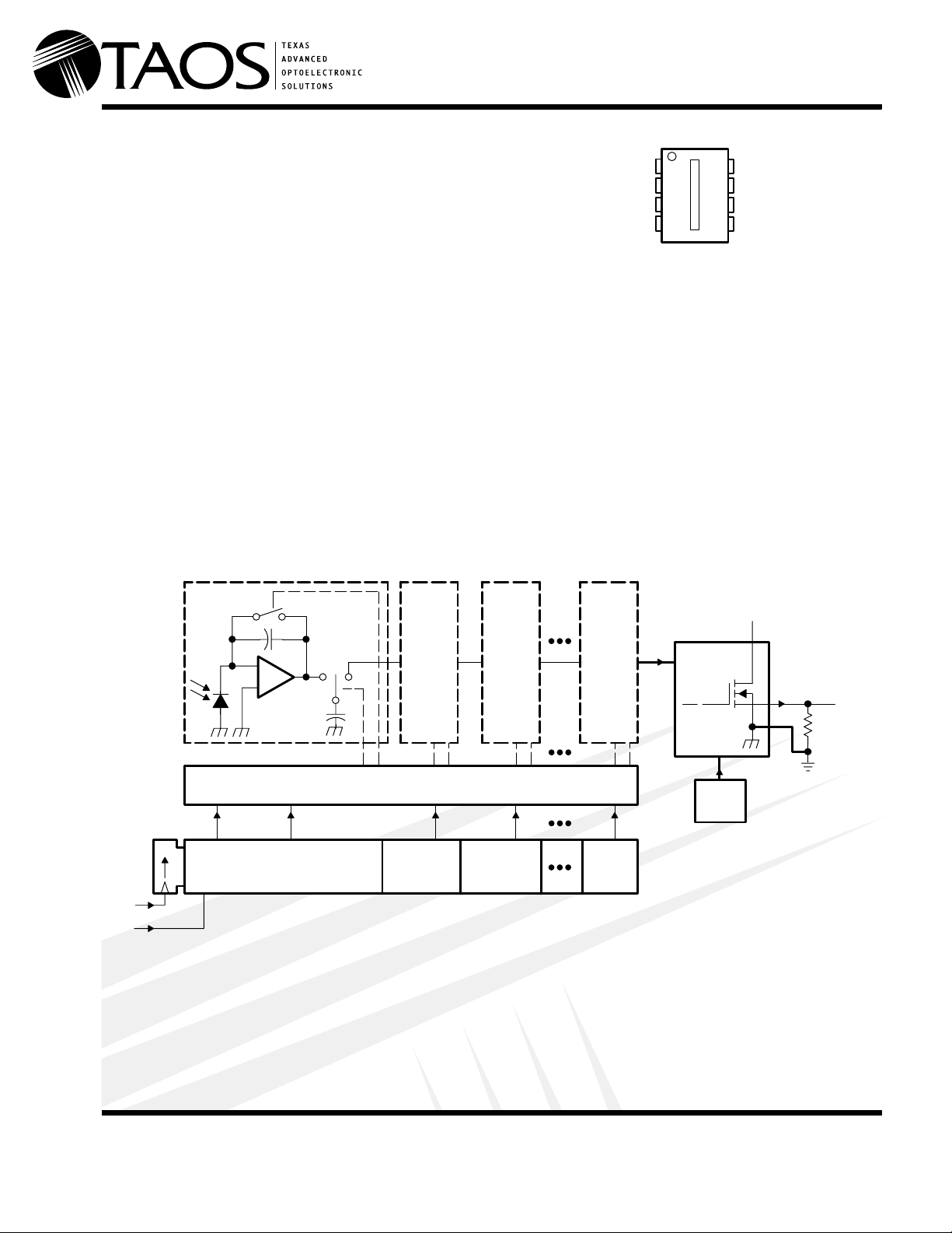
Functional Block Diagram
Pixel 1
_
+
Sample/
Output
Integrator
Reset
Pixel
2
Pixel
3
Pixel
102
Analog
Bus
Output
Amplifier
V
DD
4
6,7
3
AO
R
L
(External
Load)
Switch Control Logic
Hold
2
CLK 102-Bit Shift Register
1
SI
www.taosinc.com
Texas Advanced Optoelectronic Solutions Inc.
800 Jupiter Road, Suite 205 Plano, TX 75074 (972) 673-0759
Gain
Trim
Q3Q2Q1
Q102
Copyright 2001, TAOS Inc.
1
Page 2

TSL1301
102 × 1 LINEAR SENSOR ARRAY WITH HOLD
TAOS006B – JUNE 2001
Terminal Functions
TERMINAL
NAME NO.
AO 3 Analog output
CLK 2 Clock. The clock controls charge transfer, pixel output, and reset.
GND 6, 7 Ground (substrate). All voltages are referenced to the substrate.
NC 5, 8 No internal connection
SI 1 Serial input. SI defines the start of the data-out sequence.
V
DD
4 Supply voltage. Supply voltage for both analog and digital circuits.
DESCRIPTION
Detailed Description
The sensor consists of 102 photodiodes arranged in a linear array. Light energy impinging on a photodiode
generates photocurrent, which is integrated by the active integration circuitry associated with that pixel.
During the integration period, a sampling capacitor connects to the output of the integrator through an analog
switch. The amount of charge accumulated at each pixel is directly proportional to the light intensity and the
integration time.
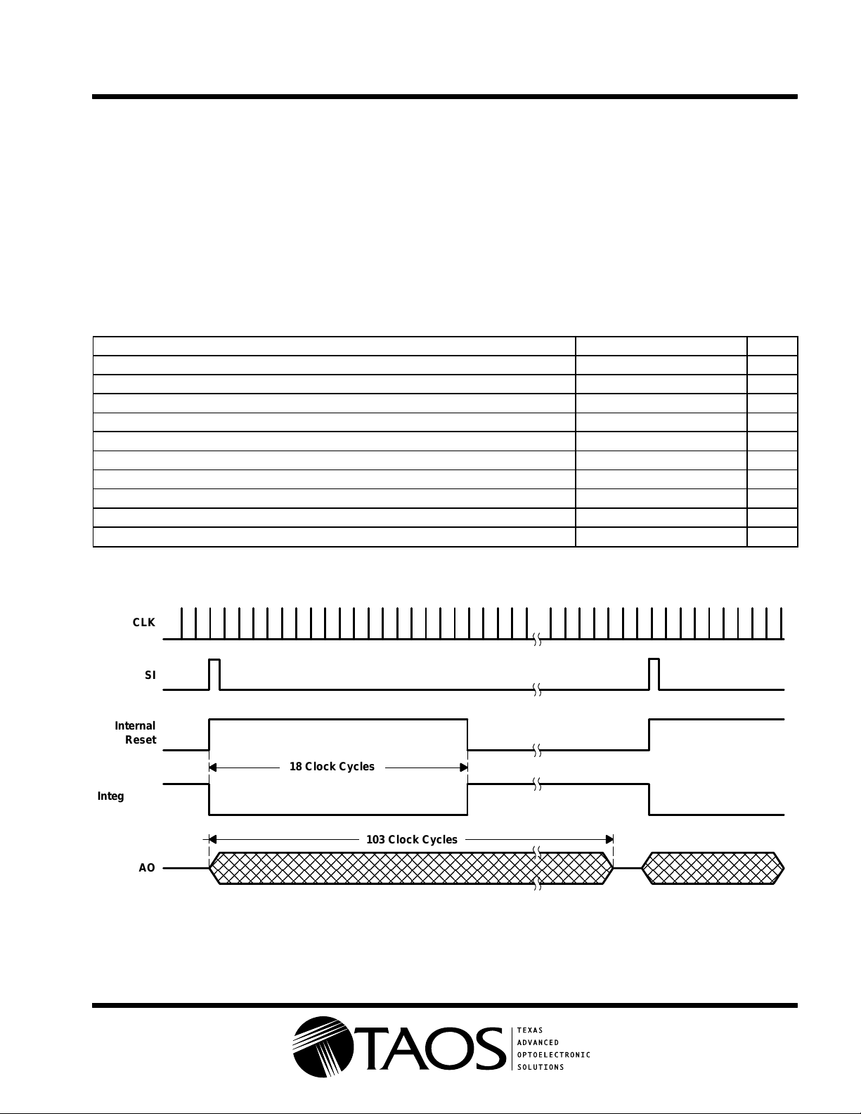
The output and reset of the integrators is controlled by a 102-bit shift register and reset logic. An output cycle
is initiated by clocking in a logic 1 on SI. An internal signal, called Hold, is generated from the rising edge of SI
and transmitted to analog switches in the pixel circuit. This causes all 102 sampling capacitors to be
disconnected from their respective integrators and starts an integrator reset period. As the SI pulse is clocked
through the shift register, the charge stored on the sampling capacitors is sequentially connected to a
charge-coupled output amplifier that generates a voltage on analog output AO. Simultaneously, during the first
18 clock cycles, all pixel integrators are reset, and the next integration cycle begins on the 19th clock. On the
103rd clock rising edge, the SI pulse is clocked out of the shift register and the analog output AO assumes a
high impedance state. Note that this 103rd clock pulse is required to terminate the output of the 102nd pixel,
and return the internal logic to a known state. A subsequent SI pulse may be presented as early as the 104th
clock pulse, thereby initiating another pixel output cycle.
AO is driven by a source follower that requires an external pulldown resistor. When the output is not in the output
phase, it is in a high-impedance state. The output is nominally 0 V for no light input and 2 V for a nominal
white-level output, with a nominal full-scale (saturation) voltage of 3 V.
The TSL1301 is intended for use in a wide variety of applications, including: image scanning, mark and code
reading, optical character recognition (OCR) and contact imaging, edge detection and positioning, and optical
linear and rotary encoding.
Copyright 2001, TAOS Inc.
2
www.taosinc.com
Page 3
TSL1301
102 × 1 LINEAR SENSOR ARRAY WITH HOLD
TAOS006B – JUNE 2001
Absolute Maximum Ratings
†
Supply voltage, VDD 7 V. . . . . . . . . . . . . . . . . . . . . . . . . . . . . . . . . . . . . . . . . . . . . . . . . . . . . . . . . . . . . . . . . . . . . . . .
Digital input current range, II –20 mA to 20 mA. . . . . . . . . . . . . . . . . . . . . . . . . . . . . . . . . . . . . . . . . . . . . . . . . . . . .
Operating free-air temperature range, TA 0°C to 70°C. . . . . . . . . . . . . . . . . . . . . . . . . . . . . . . . . . . . . . . . . . . . . .
Storage temperature range, T
–25°C to 85°C. . . . . . . . . . . . . . . . . . . . . . . . . . . . . . . . . . . . . . . . . . . . . . . . . . . .
stg
Lead temperature 1,6 mm (1/16 inch) from case for 10 seconds 260°C. . . . . . . . . . . . . . . . . . . . . . . . . . . . . . .
†
Stresses beyond those listed under “absolute maximum ratings” may cause permanent damage to the device. These are stress ratings only, and
functional operation of the device at these or any other conditions beyond those indicated under “recommended operating conditions” is not
implied. Exposure to absolute-maximum-rated conditions for extended periods may affect device reliability.
Recommended Operating Conditions (see Figure 1 and Figure 2)
MIN NOM MAX UNIT
Supply voltage, V
Input voltage, V
High-level input voltage, V
Low-level input voltage, V
Wavelength of light source, λ 400 1000 nm
Clock frequency, f
Sensor integration time, t
Setup time, serial input, t
Hold time, serial input, t
Operating free-air temperature, T
NOTE 1: SI must go low before the rising edge of the next clock pulse.
DD
I
IH
IL
clock
int
su(SI)
(see Note 1) 0 ns
h(SI)
A
4.5 5 5.5 V
0 V
VDD × 0.7 V
0 VDD × 0.3 V
5 2000 kHz
0.0425 100 ms
20 ns
0 70 °C
DD
DD
V
V
CLK
SI
Internal
Reset
Integration
AO
www.taosinc.com
18 Clock Cycles
Not Integrating Integrating
103 Clock Cycles
Figure 1. Timing Waveforms
Hi-ZHi-Z
Copyright 2001, TAOS Inc.
3
Page 4

TSL1301
102 × 1 LINEAR SENSOR ARRAY WITH HOLD
TAOS006B – JUNE 2001
Electrical Characteristics at f
R
= 330 Ω, Ee = 800 nW/cm2 (unless otherwise noted) (see Note 2)
L
PARAMETER TEST CONDITIONS MIN TYP MAX UNIT
Analog output voltage (white, average over 102 pixels) 1.6 2 2.4 V
Analog output voltage (dark, average over 102 pixels) Ee = 0 0 0.3 0.4 V
PRNU Pixel response nonuniformity Pixels 2–101, See Note 3 ±10%
Nonlinearity of analog output voltage See Note 4 ±0.5% FS
Output noise voltage Ee = 0, See Note 5 3 mVrms
Saturation exposure See Note 6 5.45 7 nJ/cm
Analog output saturation voltage 3 3.5 V
DSNU Dark signal nonuniformity
IL Image lag See Note 8 1%
I
DD
I
IH
I
IL
C
NOTES: 2. Clock duty cycle is assumed to be 50%.
Supply current 2.5 4 mA
High-level input current VI = V
Low-level input current VI = 0 10 µA
Input capacitance 5 pF
i
3. PRNU is the maximum difference between the voltage from any single pixel and the average output voltage from all pixels of the
device under test when the array is uniformly illuminated.
4. Nonlinearity is defined as the maximum deviation from a best-fit straight line over the dark-to-white irradiance levels, as a percent
of analog output voltage (white).
5. RMS noise is the standard deviation of a single-pixel output under constant illumination as observed over a 5-second period.
6. Minimum saturation exposure is calculated using the maximum responsivity and minimum output saturation voltage figures.
7. DNSU is the difference between the maximum and minimum of dark-current voltage.
8. Image lag is a residual signal left in a pixel from a previous exposure. It is defined as a percent of white-level signal remaining after
a pixel is exposed to a white condition followed by a dark condition:
VAO–V
IL
V
AO(white)
AO(dark)
V
AO(dark)
= 200 kHz, VDD = 5 V, TA = 25°C, λp = 565 nm, t
clock
All pixels,
See Note 7
DD
100
E
= 0
e
= 5 ms,
int
0.04 0.12 V
2
10 µA
Copyright 2001, TAOS Inc.
4
www.taosinc.com
Page 5

TSL1301
102 × 1 LINEAR SENSOR ARRAY WITH HOLD
TAOS006B – JUNE 2001
Operating Characteristics over recommended ranges of supply voltage and operating free-air
temperature (see Figure 2)
PARAMETER TEST CONDITIONS MIN TYP MAX UNIT
t
Clock pulse duration (high) 50 ns
w(H)
t
Clock pulse duration (low) 50 ns
w(L)
t
Analog output settling time to ±1% RL = 330 Ω, CL = 50 pF 350 ns
s
t
w
CLK
t
su(SI)
SI
1 2 102 103
50%
t
h(SI)
2.5 V
5 V
0 V
5 V
0 V
AO
t
s
Pixel 1
t
s
Pixel 102
Figure 2. Operational Waveforms
TYPICAL CHARACTERISTICS
PHOTODIODE SPECTRAL RESPONSIVITY
1
TA = 25°C
0.8
0.6
0.4
www.taosinc.com
Normalized Responsivity
0.2
0
300 500 700 900
λ – Wavelength – nm
Figure 3
1100400 600 800 1000
Copyright 2001, TAOS Inc.
5
Page 6

TSL1301
102 × 1 LINEAR SENSOR ARRAY WITH HOLD
TAOS006B – JUNE 2001
MECHANICAL INFORMATION
This dual-in-line package consists of an integrated circuit mounted on a lead frame and encapsulated with an
electrically nonconductive clear plastic compound.
0.430 (10,92)
8 Places
0.410 (10,41)
0.390 (9,91)
‡
58
0.020 (0,51) R NOM
41
4 Places
C
(pixel)
L
C
L
8° MAX TYP
0.053 (1,35)
0.043 (1,09)
Pin 1 SI
Pin 2 CLK
Pin 3 AO
Pin 4 V
DD
Pin 5 NC
Pin 6 GND
Pin 7 GND
Pin 8 NC
0.075 (1,91)
0.060 (1,52)
Centerline of Pin 1 Nominally
Lies Between Pixels 7 and 8.
0.310 (7,87)
0.290 (7,37)
0.260 (6,60)
0.240 (6,10)
10° TYP
0.030 (0,76) D NOM
0.310 (7,87)
0.290 (7,37)
0.175 (4,45)
0.155 (3,94)
0.021 (0,53)
0.060 (1,52)
0.040 (1,02)
105°
0.020 (0,51)
R MAX
4 Places
†
True position when unit is installed
‡
Minimum flat-optical-surface length
90°
8 Places
Seating Plane
0.012 (0,30)
0.008 (0,20)
0.016 (0,41)
0.014 (0,36)
0.067 (1,70)
0.053 (1,35)
NOTES: A. All linear dimensions are in inches and parenthetically in millimeters.
B. This drawing is subject to change without notice.
C. Index of refraction of clear plastic is 1.55.
Figure 4. Packaging Configuration
0.025 (0,64)
0.015 (0,38)
0.100 (2,54) T .P.
0.150 (3,81)
0.125 (3,18)
†
Copyright 2001, TAOS Inc.
6
www.taosinc.com
Page 7

TSL1301
102 × 1 LINEAR SENSOR ARRAY WITH HOLD
TAOS006B – JUNE 2001
PRODUCTION DATA — information in this document is current at publication date. Products conform to
specifications in accordance with the terms of Texas Advanced Optoelectronic Solutions, Inc. standard
warranty. Production processing does not necessarily include testing of all parameters.
NOTICE
Texas Advanced Optoelectronic Solutions, Inc. (TAOS) reserves the right to make changes to the products contained in this
document to improve performance or for any other purpose, or to discontinue them without notice. Customers are advised
to contact TAOS to obtain the latest product information before placing orders or designing TAOS products into systems.
TAOS assumes no responsibility for the use of any products or circuits described in this document or customer product
design, conveys no license, either expressed or implied, under any patent or other right, and makes no representation that
the circuits are free of patent infringement. TAOS further makes no claim as to the suitability of its products for any particular
purpose, nor does TAOS assume any liability arising out of the use of any product or circuit, and specifically disclaims any
and all liability, including without limitation consequential or incidental damages.
TEXAS ADVANCED OPTOELECTRONIC SOLUTIONS, INC. PRODUCTS ARE NOT DESIGNED OR INTENDED FOR
USE IN CRITICAL APPLICATIONS IN WHICH THE FAILURE OR MALFUNCTION OF THE TAOS PRODUCT MAY
RESUL T I N PERSONAL INJURY OR DEATH. USE OF TAOS PRODUCTS IN LIFE SUPPORT SYSTEMS IS EXPRESSLY
UNAUTHORIZED AND ANY SUCH USE BY A CUSTOMER IS COMPLETELY AT THE CUSTOMER’S RISK.
TAOS, the TAOS logo, and Texas Advanced Optoelectronic Solutions are trademarks of Texas Advanced Optoelectronic Solutions
Incorporated.
www.taosinc.com
Copyright 2001, TAOS Inc.
7
Page 8

TSL1301
102 × 1 LINEAR SENSOR ARRAY WITH HOLD
TAOS006B – JUNE 2001
Copyright 2001, TAOS Inc.
8
www.taosinc.com
 Loading...