

Page 1
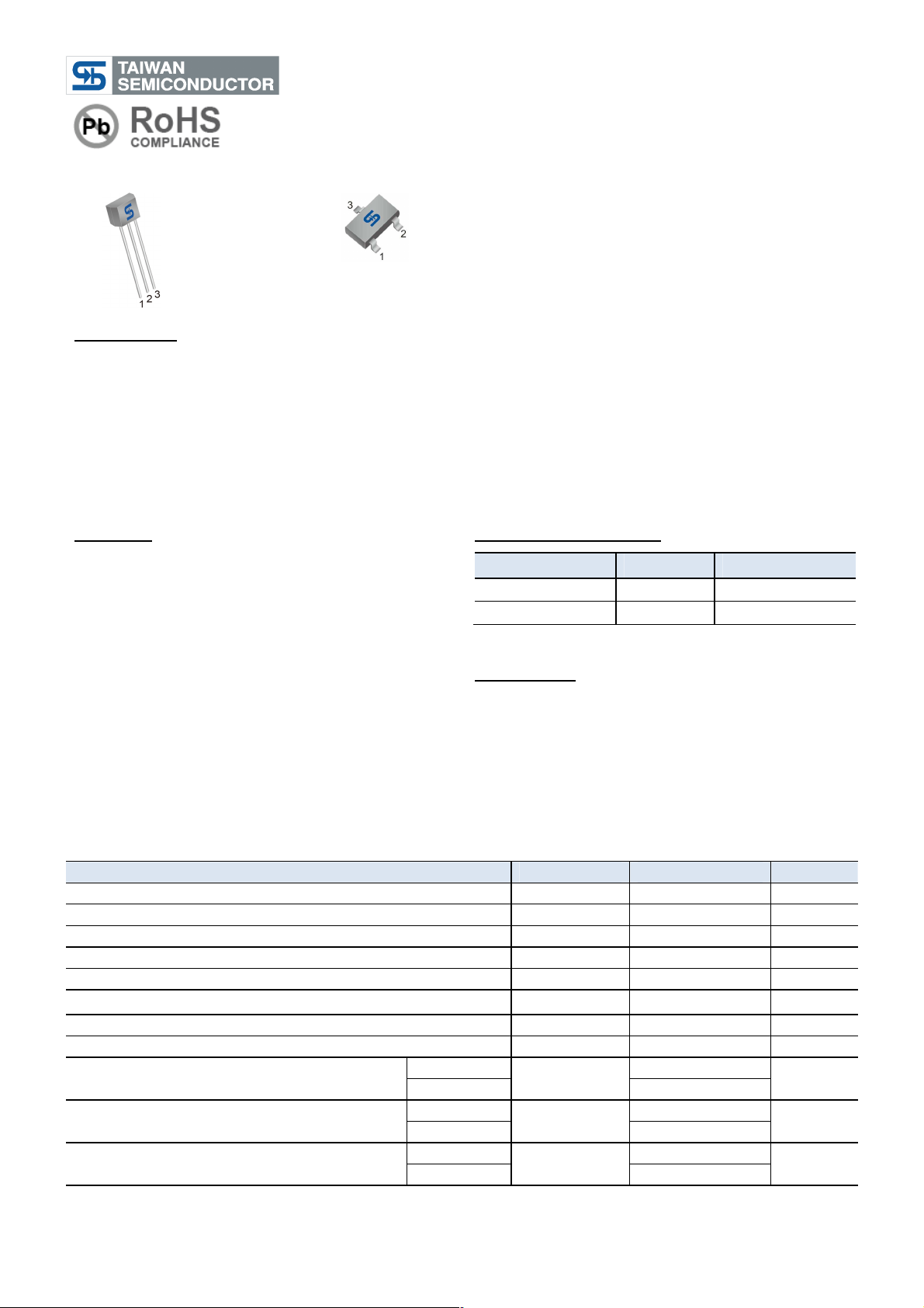
TO-92S
TSOT-23
OUT
DD
/OUT
OUT
STG
o
o
P
in
Definition
:
Pin
Definition
:
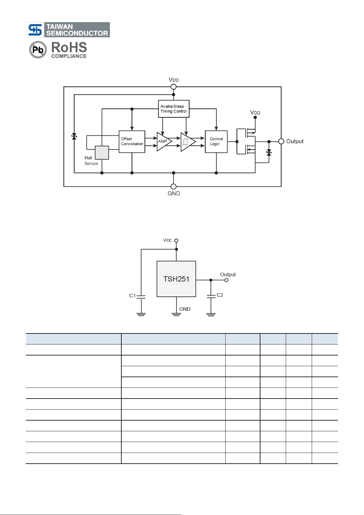
TSH251
Micropower CMOS Output Hall Effect Switch
1. VCC
2. GND
3. Output
Description
TSH251 Hall-effect sensor is a temperature stable, stress-resistant, Low Tolerance of Sensitivity micro-power
switch. Superior high-temperature performance is made possible through a dynamic offset cancellation that
utilizes chopper-stabilization. This method reduces the offset voltage normally caused by device over molding,
temperature dependencies, and thermal stress. TSH251 is special made for low operation voltage, 1.65V, to
active the chip which is includes the following on a single silicon chip: voltage regulator, Hall voltage generator,
small-signal amplifier, chopper stabilization, Schmitt trigger, CMOS output driver. Advanced CMOS wafer
fabrication processing is used to take advantage of low-voltage requirements, component matching, very low
input-offset errors, This device requires the presence of omni-polar magnetic fields for operation.
1. VCC
2. Output
3. GND
Features
● CMOS Hall IC Technology
● Strong RF noise protection
● 1.65 to 3.5V for battery-powered applications
● Omni polar, output switches with absolute value of
North or South pole from magnet
● Operation down to 1.65V, Micropower consumption
● High Sensitivity for reed switch replacement
applications
● Low sensitivity drift in crossing of Temp. range
● Ultra Low power consumption at 5uA (Avg)
● High ESD Protection, HBM > ±4KV( min )
● Totem-pole output
Absolute Maximum Rating
Characteristics
Supply voltage
Output Voltage
Reverse Voltage
Magnetic flux density
Output current
Operating temperature range
Storage temperature range
Maximum Junction Temp
Thermal Resistance - Junction to Ambient
Thermal Resistance - Junction to Case
Package Power Dissipation
Note: Exceeding the absolute maximum ratings may cause permanent damage. Exposure to absolute maximum-
rated conditions for extended periods may affect device reliability.
(Ta = 25oC unless otherwise noted)
TO-92S
TSOT-23
TO-92S
TSOT-23
TO-92S
TSOT-23
Ordering Information
Part No. Package Packing
TSH251CT B0G TO-92S 1Kpcs / Bulk Bag
TSH251CX RFG TSOT-23 3Kpcs / 7” Reel
Note: “G” denote for Halogen Free Product
Application
● Solid state switch
● Handheld Wireless Handset Awake Switch
(Flip Cell/PHS Phone/Note Book/Flip Video Set)
● Lid close sensor for battery powered devices
● Magnet proximity sensor for reed switch
replacement in low duty cycle applications
● Water Meter, Floating Meter
Limit Value
4.5
4.5
-0.3
Unlimited
1
-40 to +85
-65 to +150
150
206
543
148
410
606
230
V
VDD
V
I
T
OPR
T
TJ
θJA
θJC
PD
Unit
V
V
V
Gauss
mA
o
C
C
C
o
C/W
o
C/W
mW
1/8
Version: A13
Page 2
TSH251
Micropower CMOS Output Hall Effect Switch
Block Diagram
Note: Static sensitive device; please observe ESD precautions. Reverse VDD protection is not included. For
reverse voltage protection, a 100Ω resistor in series with VDD is recommended.
Typical Application Circuit
C1:10nF
C2:100pF
Electrical Specifications (
Parameters Test Conditions Min Typ Max Units
Supply Voltage Operating 1.65 -- 3.5 V
Supply Current
Output Leakage Current Output off -- -- 1 uA
Output High Voltage IOUT=0.5mA(Source) VDD-0.2
DC Operating Parameters:TA=+25oC,VDD=1.8V)
Awake State -- 1.4 3 mA
Sleep State -- 3.6 7 µA
Average -- 5 10 µA
-- -- V
Output Low Voltage IOUT=0.5mA(Sink) -- -- 0.2 V
Awake mode time Operating -- 40 80 uS
Sleep mode time Operating -- 40 80 mS
Duty Cycle -- 0.1 -- %
Electro-Static Discharge HBM 4 KV
2/8
Version: A13
Page 3
Micropower CMOS Output Hall Effect Switch
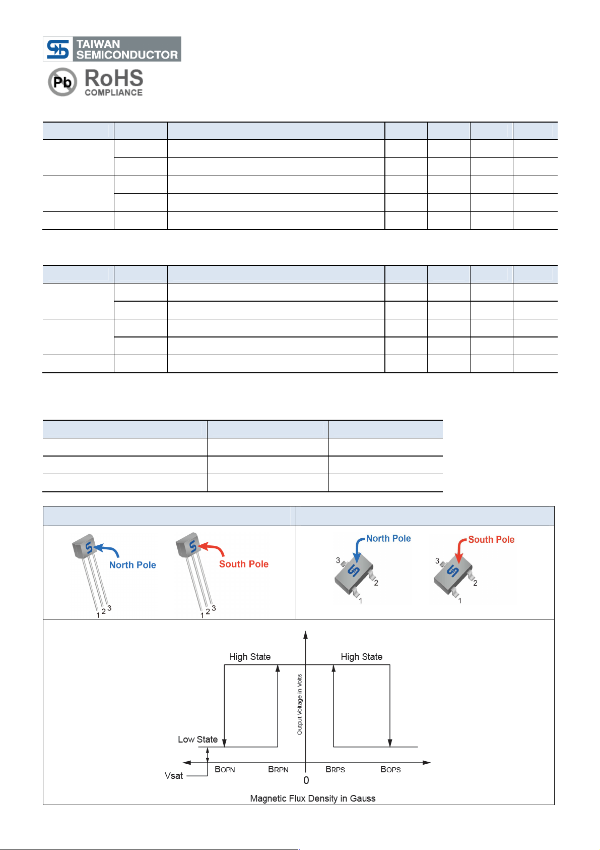
Magnetic Specifications (TSH251CT)
Parameter Symbol
B
S pole to branded side, B > BOP, Vout On 30 55 Gauss
Operating
Point
Release
Point
Hysteresis
Note: 1G (Gauss) = 0.1mT (millitesta)
OPS
B
N pole to branded side, B > BOP, Vout On -55 -30 Gauss
OPN
B
S pole to branded side, B < BRP, Vout Off 10 20 Gauss
RPS
B
N pole to branded side, B < BRP, Vout Off -20 -10 Gauss
RPN
B
|BOPx - BRPx| 10 Gauss
HYS
Magnetic Specifications (TSH251CX)
Parameter Symbol
B
N pole to branded side, B > BOP, Vout On 30 55 Gauss
Operating
Point
Release
Point
Hysteresis
Note: 1G (Gauss) = 0.1mT (millitesta)
OPS
B
S pole to branded side, B > BOP, Vout On -55 -30 Gauss
OPN
B
N pole to branded side, B < BRP, Vout Off 10 20 Gauss
RPS
B
S pole to branded side, B < BRP, Vout Off -20 -10 Gauss
RPN
B
|BOPx - BRPx| 10 Gauss
HYS
Test Conditions Min. Typ. Max. Units
Test Conditions Min. Typ. Max. Units
TSH251
Output Behavior versus Magnetic Pole
DC Operating Parameters: TA = -40 to 125oC, VCC = 1.8V ~ 6V
Parameter Test condition OUT
South pole
Null or weak magnetic field
North pole
B<Bop[(-55)~(-10)] Low
B=0 or B < BRP High
B>Bop(55~10) Low
TO-92S SOT-23
3/8
Version: A13
Page 4

Characteristic Performance
TSH251
Micropower CMOS Output Hall Effect Switch
Figure 1. Supply Voltage vs. Flux Density
Figure 3. Supply Current vs. Temperature
Figure 2. Temperature vs. Flux Density
Figure 4. Supply Current vs. Supply Voltage
Figure 5. Output Saturation Voltage vs.
Supply Voltage
4/8
Figure 6. Output Saturation Voltage vs.
Temperature
Version: A13
Page 5

Characteristic Performance
TSH251
Micropower CMOS Output Hall Effect Switch
Figure 7. Output Leakage Current vs.
Supply Voltage
Figure 8. Power Dissipation vs. Temperature
5/8
Version: A13
Page 6

TSH251
Micropower CMOS Output Hall Effect Switch
TO-92S Mechanical Drawing
Marking Diagram
251 = Device Code
Y = Year Code (3=2013, 4=2014….)
WW = Week Code (01~52)
Unit: Millimeters
6/8
Version: A13
Page 7

TSH251
Micropower CMOS Output Hall Effect Switch
TSOT-23 Mechanical Drawing
Marking Diagram
251 = Device Code
WW = Week Code Table
Unit: Millimeters
week 1 2 3 4 5 6 7 8 9 10 11 12 13
code OA OB OC OD OE OF OG OH OI OJ OK OL OM
week 14 15 16 17 18 19 20 21 22 23 24 25 26
code ON OO OP OQ OR OS OT OU OV OW OX OY OZ
week 27 28 29 30 31 32 33 34 35 36 37 38 39
code PA PB PC PD PE PF PG PH PI PJ PK PL PM
week 40 41 42 43 44 45 46 47 48 49 50 51 52
code PN PO PP PQ PR PS PT PU PV PW PX PY PZ
7/8
Version: A13
Page 8

TSH251
Micropower CMOS Output Hall Effect Switch
Notice
Specifications of the products displayed herein are subject to change without notice. TSC or anyone on its behalf,
assumes no responsibility or liability for any errors or inaccuracies.
Information contained herein is intended to provide a product description only. No license, express or implied, to
any intellectual property rights is granted by this document. Except as provided in TSC’s terms and conditions of
sale for such products, TSC assumes no liability whatsoever, and disclaims any express or implied warranty,
relating to sale and/or use of TSC products including liability or warranties relating to fitness for a particular purpose,
merchantability, or infringement of any patent, copyright, or other intellectual property right.
The products shown herein are not designed for use in medical, life-saving, or life-sustaining applications.
Customers using or selling these products for use in such applications do so at their own risk and agree to fully
indemnify TSC for any damages resulting from such improper use or sale.
8/8
Version: A13
Page 9

 Loading...