

Page 1
TSH22
HIGH PERFORMANCE
DUALBIPOLAR OPERATIONALAMPLIFIER
June 1998
1
2
3
4
5
6
7
8
-
+
-
+
Output 1
Inverting input 1
Non-inverting input 1
V
CC
V
CC
Output 2
Inverting input 2
Non-inverting input2
-
+
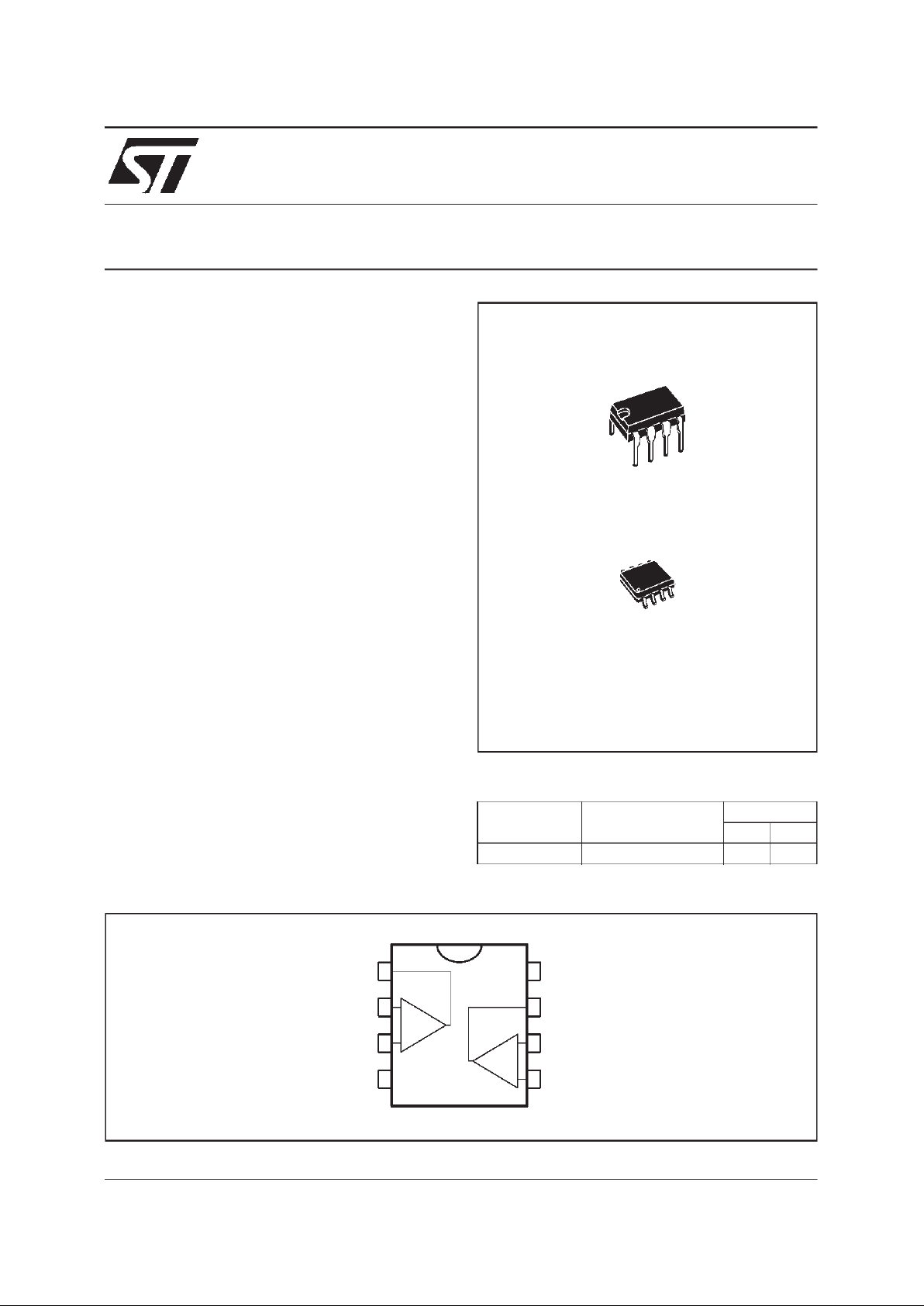
PINCONNECTIONS (topview)
N
DIP8
(Plastic Package)
.
HIGHGAIN BANDWIDTH PRODUCT : 25MHz
.
HIGHSLEW RATE : 15V/µµs
.
SINGLEOR DUAL SUPPLYOPERATION:
3V TO30V (±1.5Vto ±15V)
.
LOW VOLTAGE NOISE : 14nV/√√Hz
.
NO PHASE INVERSION
.
ESD TOLERANCE: 2kV
.
LATCH-UP IMMUNITY
.
SPICE MACROMODEL INCLUDED IN THIS
SPECIFICATION
D
SO8
(Plastic Micropackage)
ORDER CODES
Part Number Temperature Range
Package
ND
TSH22I -40, +125
o
C ••
DESCRIPTION
TheTSH22 is a dual bipolar operational amplifier
offering a single supply operation from 3V to 30V
with very good performances : medium speed
(25MHz),unity gain stability and low noise.
The TSH22isthereforean enhancedreplacement
of standard dual operationalamplifiers.
1/11
Page 2
ABSOLUTE MAXIMUM RATINGS
Symbol Parameter Value Unit
V
CC
Supply Voltage ±18 or +36 V
V
id
Differential Input Voltage - (note 1) ±36 V
V
i
Input Voltage - (note 1) ±18 V
Output Short-Circuit Duration - (note 2) Infinite
T
oper
Operating Free-air Temperature Range -40 to +125
o
C
T
j
Maximum Junction Temperature +150
o
C
T
stg
Storage Temperature -65 to +150
o
C
P
tot
Maximum Power Dissipation -(note 2) 500 mW
Notes : 1. Either or both input voltages must not exceed the magnitude of V
CC
+
or V
CC
-
2. Power dissipation mustbe considered to ensure maximum junction temperature (Tj) is notexceeded
OPERATINGCONDITIONS
Symbol Parameter Value Unit
V
CC
Supply Voltage 3 to 30 V
Non Inve rting
Input
Inverting Inpu t
20
µ
A
250µA
Cc
Output
ESD
ESD
V
cc
+
V
cc
-
20
µA
130
µ
A
130
µ
A
600
µA
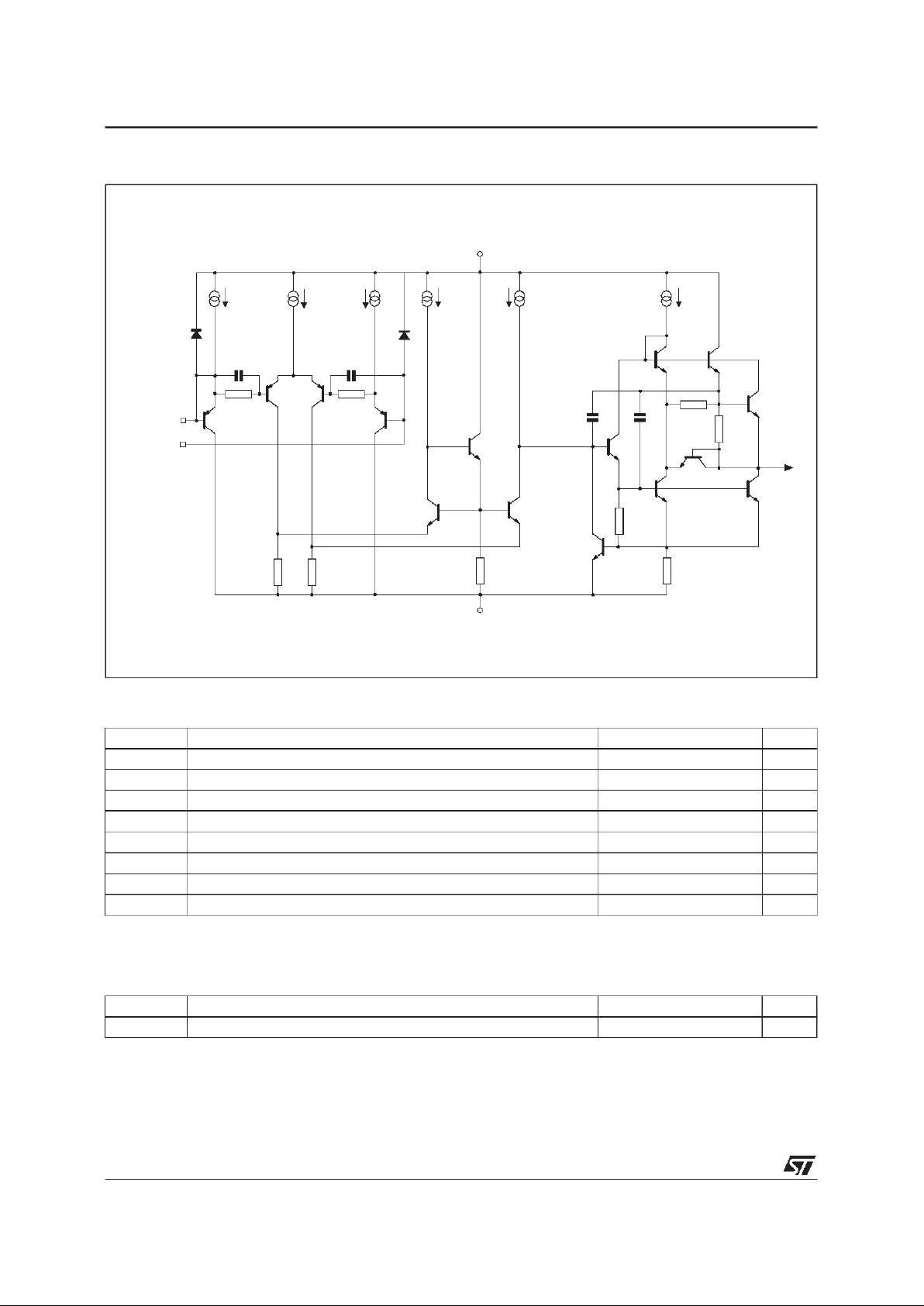
SCHEMATIC DIAGRAM (1/2 TSH22)
TSH22
2/11
Page 3

ELECTRICALCHARACTERISTICS
V
CC
+
= +15V,V
CC
-
=-15V,T
amb
=25°C(unlessotherwisespecified)
Symbol Parameter Min. Typ. Max. Unit
V
io
Input Offset Voltage (Vic= 0V, Vo= 0V)
V
CC
+
= +15V, V
CC
-
= -15V
T
min.
≤ T ≤ T
max.
V
CC
+
= +5V, V
CC
-
=0V
2.5
3.5
2.5
mV
∆V
io
Input Offset Voltage Drift (Vic= 0V, Vo= 0V) 2 µV/oC
I
io
Input Offset Current (Vic= 0V, VO= 0V) 3 65 nA
I
ib
Input Bias Current (Vic= 0V, VO= 0V) 100 650 nA
V
icm
Common Mode Input Voltage Range V
CC
-
to
V
CC
+
-1.8V
V
A
vd
Large Signal Voltage Gain (RL=2kΩ,VO= 0V to +10V)
T
min.
≤ T ≤ T
max.
32
20
100 V/mV
±V
opp
Output Voltage Swing (Vid= ±1V)
V
CC
+
= +15V, V
CC
-
= -15V RL=2kΩ V
OH
V
OL
RL= 10kΩ V
OH
V
OL
V
CC
+
= +5V, V
CC
-
=0V RL=2kΩ V
OH
V
OL
13.4
13.4
3.7
13.9
-13.9
14
-14.7
0.15
-13.5
-14.1
0.2
V
I
o
Output Short Circuit Current
(V
id
= ±1V, Vo= 0V) Source
Sink
25
25
37
37
mA
CMR Common Mode Rejection Ratio (V
ic
= -15V to +13.2V) 80 100 dB
SVR Supply Voltage Rejection Ratio
V
CC
+
/V
CC
-
= +15V / -15V to +5V / -5V 90 105
dB
I
CC
Supply Current (VO= 0V, no load, each amplifier)
V
CC
+
= +15V, V
CC
-
= -15V
T
min.
≤ T ≤ T
max.
V
CC
+
= +5V, V
CC
-
=0V
2.15 2.75
3
2.75
mA
SR Slew Rate
(V
i
= -10V to +10V,CL= 100pF, RL=2kΩ,AV= +1) 8 15
V/µs
GBP Gain Bandwidth Product (f = 100kHz, R
L
=2kΩ,CL= 100pF) 17 25 MHz
B Unity Gain Bandwidth (Open loop) 5 MHz
∅m Phase Margin R
L
=2kΩ
R
L
=2kΩ,CL= 100pF
50
40
Degrees
e
n
Equivalent Input Noise Voltage (RS= 100Ω, f = 1kHz) 14 nV/√Hz
V
O1/VO2
Channel Separation (f = 20Hz to 20kHz) 120 dB
THD Total Harmonic Distortion
(V
CC
=±15V,f = 1kHz, A
VCL
= 20dB, RL= 600Ω,Vo= 3Vrms) 0.003
%
TSH22
3/11
Page 4
** StandardLinear Ics Macromodels,1993.
CONNECTIONS :
* 1 INVERTINGINPUT
* 2 NON-INVERTINGINPUT
* 3 OUTPUT
* 4 POSITIVEPOWERSUPPLY
* 5 NEGATIVEPOWERSUPPLY
.SUBCKTTSH221 3 2 4 5 (analog)
*********************************************************
.MODEL MDTH D IS=1E-8 KF=7.976636E-15
CJO=10F
* INPUTSTAGE
CIP 2 5 1.200000E-11
CIN 1 5 1.200000E-11
EIP 10 5 2 5 1
EIN 16 5 1 5 1
RIP 10 11 1.083333E+00
RIN 15 16 1.083333E+00
RIS 1115 8.942641E+00
DIP 1112 MDTH 400E-12
DIN 15 14 MDTH400E-12
VOFP12 13 DC 0
VOFN 1314 DC 0
IPOL 13 5 2.400000E-04
CPS 1115 10.5E-09
DINN 17 13 MDTH 400E-12
VIN 17 5 -0.200000e+00
DINR 15 18 MDTH 400E-12
VIP 4 18 1.800000E+00
FCP4 5 VOFP7.750000E+00
FCN 5 4 VOFN 7.750000E+00
FIBP2 5 VOFN 5.000000E-04
FIBN 5 1 VOFP5.000000E-04
* AMPLIFYINGSTAGE
FIP 5 19 VOFP 6.708333E+02
FIN 5 19 VOFN 6.708333E+02
GVNEG5 19 5 13 1.395908E-05
GVPOS5 19 4 13 1.395908E-05
RG1 19 5 8.056996E+04
RG2 19 4 8.056996E+04
CC 19 29 1.100000E-08
HZTP30 29VOFP6.545046E+01
HZTN 530 VOFN 6.545046E+01
DOPM19 22 MDTH 400E-12
DONM 21 19 MDTH400E-12
HOPM22 28 VOUT 4.054054E+03
VIPM28 4 1.500000E+02
HONM 21 27 VOUT4.054054E+03
VINM 5 27 1.500000E+02
RPM1 5 80 1E+06
RPM2 4 80 1E+06
GAVPH5 82 1980 6.00E-07
RAVPHGH82 4 3333222
RAVPHGB82 5 3333222
RAVPHDH82 831000000
RAVPHDB82 84 1000000
CAVPHH4 83 0.12243E-12
CAVPHB5 84 0.12243E-12
EOUT26238251
VOUT23 5 0
ROUT 26 3 2.472597E+01
COUT 3 5 1.000000E-12
DOP 19 25 MDTH400E-12
VOP4 25 1.824860E+00
DON 24 19 MDTH 400E-12
VON 24 5 1.824860E+00
.ENDS
MACROMODEL
ELECTRICALCHARACTERISTICS
V
CC
= ±15V, T
amb
=25oC (unlessotherwisespecified)
Symbol Conditions Value Unit
V
id
0mV
A
vd
RL=2kΩ 100 dB
I
CC
No load, per operator 2 mA
V
icm
-15.2 to 13.8 V
V
OH
RL=2kΩ +13.9 V
V
OL
RL=2kΩ -13.9 V
I
sink
VO=0V 40 mA
I
source
VO=0V 40 mA
GBP R
L
=2k
Ω,
CL= 100pF 34 MHz
SR R
L
=2k
Ω,
CL= 100pF 10 V/µs
∅mR
L
=2k
Ω,
CL= 100pF 36 Degrees
∅mR
L
=2k
Ω,
CL= 300pF 26 Degrees
TSH22
4/11
Page 5

APPLICATIONSINFORMATION
TSH22 IN COMPARATOR APPLICATION
The TSH22 is a dual high performances operational amplifier featuring speed of 30MHz and single supply operation from 3Vto 30V.
Most of operational amplifiers are not suited for
comparator use because of low transition speed,
output signal incompatible with standard logics
level and mainly, phase inversion.
The phaseinversionoccureswhena strong differential signal is applied to the device inputs. The
output level is then inverted and shows a wrong
logic state.
TSH22 does not present this problematic
behaviour.
Displayedcurves below showthe deviceresponse
in standardcomparatorconfigurationwithoutexternal components.
Transitionspeed : Typicaltransitionspeedundera
single 5V supply voltage is about 2µs from 50mV
overdrive. V
OH
min. is 3.7V and VOLmax. is 0.2V
(2kΩ load)makingitcompatiblewithstandardlogic
families.
Figures 3 & 4 show output signal transition for a
50mV and 250mV input signal overdrive respectively of 3µs and1µs.
Vin+
Vref
+5V
Vout
2k
Ω
TS H22
Figure 1 : Basiccomparator application Figure2 : Operatingconditions
Figure 3 : Transitionspeed @50mV overdrive Figure4 : Transition speed @ 250mV overdrive
TSH22
5/11
Page 6

8
6
4
2
0
-2
-4
-6
-8
Time (50µs/div)
Input & Ouput Voltages, V
id
(V), V
o
(V)
V
id
V
o
Figure6 : Saturationbehaviourwith15MHz
standardoperational amplifier
Figure 5 : Behaviourwith TSH22
At high differentialinputvoltage, the TSH22 keeps
the right output level thanks to its specific input
structures.
The advantage is obvious on the following figures
and can be also an advantagein linear use when
saturationmight occure.
Figure 5 & 6 show the behaviour in follower stage
with saturation output of TSH22 versus 15MHz
standardoperationalamplifier.
PHASE INVERSION
TSH22
6/11
Page 7

0.4
0.3
0.2
0.1
0
-0.1
-0.2
-0.3
-0.4
-50 -25 0 25 50 75 100 125
Temperature, T
amb
(°C)
Input Offset Voltage, V
io
(mV)
INPUT OFFSET VOLTAGEDRIFT VERSUS
TEMPERATURE
SUPPLY CURRENT VERSUS SUPPLY
VOLTAGE(BOTH OP-AMP)
50
45
40
35
30
25
20
15
10
5
0
-15-12-9-6-303691215
T
amb
=25°C
V
cc
= ±
15V
Vid=1V
Applied Output Voltage, V
o
(V)
Output Sink Current,I
sink
(mA)
SINK CURRENT SOURCE CURRENT
20
15
10
5
0
-5
-10
-15
-20
Time (0.5µs/div)
Output Voltage, V
o
(V)
T
amb
=25°
C
Vcc= ±15V
A
v
=
+1
RL=2kΩ
CL= 100pF
SLEW RATE @ 30V
T
amb
=25°
C
Vcc=
+2V/-1V
Av= +1
RL=2kΩ
CL= 100pF
0.8
0.6
0.4
0.2
0
-0.2
-0.4
-0.6
-0.8
Time (0.2µs/div)
Output Voltage, V
o
(V)
SLEWRATE @ 3V
TSH22
7/11
Page 8

SMALL SIGNAL RESPONSE@ 30V SMALLSIGNALRESPONSE @ 3V
20
15
10
5
0
-5
-10
-15
-20
-0.4
Output Voltage, V
o
(V)
Differential Input Voltage, Vid(mV)
T
amb
=25°C
V
cc
= ±15V
No Load
-0.3 -0.2 -0.1 0 0.1 0.2 0.3 0.4
LARGE SIGNAL VOLTAGE GAIN @ NO LOAD LARGESIGNALVOLTAGE GAIN @ LOAD
UNITY GAIN BANDWIDTH @ 30V
10k 100k 1M 10M
45
40
35
30
25
20
15
10
5
0
-5
0
30
60
90
120
150
180
Phase
Gain
Frequency, F(Hz)
Voltage Gain (dB)
Phase (degrees)
T
amb
=25°
C
Vcc=
+2V/-1V
A
VCL
= 100
R
L
=2kΩ
CL= 100pF
UNITY GAIN BANDWIDTH @ 3V
TSH22
8/11
Page 9

21
18
15
12
9
6
3
0
-3
-6
-9
100k 1M 10M
Frequency, F(Hz)
Voltage Gain(dB)
T
amb
=25°C
Vcc= ±15V
A
VCL
= 5,2,1
RL=2kΩ
CL=100pF
A
VCL
=+5
A
VCL
=+2
A
VCL
=+1
CLOSED LOOPBANDWIDTH @ 30V
21
18
15
12
9
6
3
0
-3
-6
-9
100k 1M 10M
Frequency, F (Hz)
Voltage Gain(dB)
T
amb
=25°C
Vcc= +2V/-1V
A
VCL
= 5,2,1
RL=2kΩ
CL= 100pF
A
VCL
=+5
A
VCL
=+2
A
VCL
=+1
CLOSEDLOOPBANDWIDTH @ 3V
TSH22
9/11
Page 10

PACKAGE MECHANICAL DATA
8 PINS - PLASTICDIP
Dimensions
Millimeters Inches
Min. Typ. Max. Min. Typ. Max.
A 3.32 0.131
a1 0.51 0.020
B 1.15 1.65 0.045 0.065
b 0.356 0.55 0.014 0.022
b1 0.204 0.304 0.008 0.012
D 10.92 0.430
E 7.95 9.75 0.313 0.384
e 2.54 0.100
e3 7.62 0.300
e4 7.62 0.300
F 6.6 0260
i 5.08 0.200
L 3.18 3.81 0.125 0.150
Z 1.52 0.060
TSH22
10/11
Page 11

PACKAGE MECHANICAL DATA
8 PINS- PLASTICMICROPACKAGE (SO)
Information furnished is believed to be accurate and reliable. However, STMicroelectronics assumes no responsibility for the
consequences of use of such information nor for any infringement of patents or other rights of third parties which may result from
its use. No license is granted by implication or otherwise under any patent or patent rights of STMicroelectronics. Specifications
mentioned in this publication are subject to change without notice. This publication supersedes and replaces all information
previously supplied.STMicroelectronics productsarenot authorizedfor useas criticalcomponents inlife supportdevices orsystems
without express written approval of STMicroelectronics.
The ST logo is a trademark of STMicroelectronics
1998 STMicroelectronics – Printed in Italy – All Rights Reserved
STMicroelectronics GROUP OF COMPANIES
Australia- Brazil - Canada - China - France- Germany - Italy - Japan - Korea - Malaysia - Malta - Mexico - Morocco
The Netherlands - Singapore - Spain - Sweden - Switzerland - Taiwan - Thailand - United Kingdom - U.S.A.
Dimensions
Millimeters Inches
Min. Typ. Max. Min. Typ. Max.
A 1.75 0.069
a1 0.1 0.25 0.004 0.010
a2 1.65 0.065
a3 0.65 0.85 0.026 0.033
b 0.35 0.48 0.014 0.019
b1 0.19 0.25 0.007 0.010
C 0.25 0.5 0.010 0.020
c1 45
o
(typ.)
D 4.8 5.0 0.189 0.197
E 5.8 6.2 0.228 0.244
e 1.27 0.050
e3 3.81 0.150
F 3.8 4.0 0.150 0.157
L 0.4 1.27 0.016 0.050
M 0.6 0.024
S8
o
(max.)
TSH22
11/11
 Loading...