

Page 1

TSB12LV42 (DVLynx)
IEEE 1394-1995 Link-Layer Controller
for Digital Video
SLLS293
December 1998
Printed on Recycled Paper
Page 2

IMPORTANT NOTICE
T exas Instruments and its subsidiaries (TI) reserve the right to make changes to their products or to discontinue
any product or service without notice, and advise customers to obtain the latest version of relevant information
to verify, before placing orders, that information being relied on is current and complete. All products are sold
subject to the terms and conditions of sale supplied at the time of order acknowledgement, including those
pertaining to warranty, patent infringement, and limitation of liability.
TI warrants performance of its semiconductor products to the specifications applicable at the time of sale in
accordance with TI’s standard warranty. Testing and other quality control techniques are utilized to the extent
TI deems necessary to support this warranty . Specific testing of all parameters of each device is not necessarily
performed, except those mandated by government requirements.
CERT AIN APPLICATIONS USING SEMICONDUCTOR PRODUCTS MA Y INVOLVE POTENTIAL RISKS OF
DEATH, PERSONAL INJURY, OR SEVERE PROPERTY OR ENVIRONMENTAL DAMAGE (“CRITICAL
APPLICATIONS”). TI SEMICONDUCTOR PRODUCTS ARE NOT DESIGNED, AUTHORIZED, OR
WARRANTED TO BE SUITABLE FOR USE IN LIFE-SUPPORT DEVICES OR SYSTEMS OR OTHER
CRITICAL APPLICA TIONS. INCLUSION OF TI PRODUCTS IN SUCH APPLICATIONS IS UNDERST OOD TO
BE FULLY AT THE CUSTOMER’S RISK.
In order to minimize risks associated with the customer’s applications, adequate design and operating
safeguards must be provided by the customer to minimize inherent or procedural hazards.
TI assumes no liability for applications assistance or customer product design. TI does not warrant or represent
that any license, either express or implied, is granted under any patent right, copyright, mask work right, or other
intellectual property right of TI covering or relating to any combination, machine, or process in which such
semiconductor products or services might be or are used. TI’s publication of information regarding any third
party’s products or services does not constitute TI’s approval, warranty or endorsement thereof.
Copyright 1998, Texas Instruments Incorporated
Page 3

Contents
Section Title Page
1 Introduction 1–1. . . . . . . . . . . . . . . . . . . . . . . . . . . . . . . . . . . . . . . . . . . . . . . . . . . . . . . . . . . . . . .
1.1 TSB12L V42 1–1. . . . . . . . . . . . . . . . . . . . . . . . . . . . . . . . . . . . . . . . . . . . . . . . . . . . . . . . . . .
1.2 TSB12LV42 Features 1–2. . . . . . . . . . . . . . . . . . . . . . . . . . . . . . . . . . . . . . . . . . . . . . . . . . .
1.3 DVLynx Pinout 1–3. . . . . . . . . . . . . . . . . . . . . . . . . . . . . . . . . . . . . . . . . . . . . . . . . . . . . . . .
1.4 Ordering Information 1–3. . . . . . . . . . . . . . . . . . . . . . . . . . . . . . . . . . . . . . . . . . . . . . . . . . .
1.5 TSB12LV42 Terminal Functions 1–4. . . . . . . . . . . . . . . . . . . . . . . . . . . . . . . . . . . . . . . . . .
1.5 TSB12LV42 Terminal Functions (Continued) 1–5. . . . . . . . . . . . . . . . . . . . . . . . . . . . . . .
2 Architecture 2–1. . . . . . . . . . . . . . . . . . . . . . . . . . . . . . . . . . . . . . . . . . . . . . . . . . . . . . . . . . . . . . .
2.1 Bulky Data Interface 2–1. . . . . . . . . . . . . . . . . . . . . . . . . . . . . . . . . . . . . . . . . . . . . . . . . . . .
2.2 Bulky Data FIFO 2–1. . . . . . . . . . . . . . . . . . . . . . . . . . . . . . . . . . . . . . . . . . . . . . . . . . . . . . .
2.2.1 Bulky DV Transmit FIFO (BDTX) 2–2. . . . . . . . . . . . . . . . . . . . . . . . . . . . . . . . . . .
2.2.2 Bulky DV Receive FIFO (BDRX) 2–2. . . . . . . . . . . . . . . . . . . . . . . . . . . . . . . . . . .
2.2.3 Bulky Asynchronous Transmit FIFO (BATX) 2–2. . . . . . . . . . . . . . . . . . . . . . . . .
2.2.4 Bulky Asynchronous Receive FIFO (BARX) 2–2. . . . . . . . . . . . . . . . . . . . . . . . .
2.2.5 Bulky Isochronous Transmit FIFO (BITX) 2–2. . . . . . . . . . . . . . . . . . . . . . . . . . . .
2.2.6 Bulky Isochronous Receive FIFO (BIRX) 2–2. . . . . . . . . . . . . . . . . . . . . . . . . . . .
2.3 DV Transmit and Receive Control 2–2. . . . . . . . . . . . . . . . . . . . . . . . . . . . . . . . . . . . . . . .
2.4 Microprocessor/Microcontroller Interface 2–3. . . . . . . . . . . . . . . . . . . . . . . . . . . . . . . . . .
2.5 Control FIFO 2–3. . . . . . . . . . . . . . . . . . . . . . . . . . . . . . . . . . . . . . . . . . . . . . . . . . . . . . . . . .
2.5.1 Asynchronous Control Transmit FIFO (ACTX) 2–3. . . . . . . . . . . . . . . . . . . . . . .
2.5.2 Asynchronous Control Receive FIFO (ACRX) 2–3. . . . . . . . . . . . . . . . . . . . . . . .
2.5.3 Broadcast Write Receive FIFO (BWRX) 2–3. . . . . . . . . . . . . . . . . . . . . . . . . . . . .
2.6 Physical Layer 2–3. . . . . . . . . . . . . . . . . . . . . . . . . . . . . . . . . . . . . . . . . . . . . . . . . . . . . . . . .
2.7 Configuration Register (CFR) 2–3. . . . . . . . . . . . . . . . . . . . . . . . . . . . . . . . . . . . . . . . . . . .
3 Functional Description and Data Formats 3–1. . . . . . . . . . . . . . . . . . . . . . . . . . . . . . . . . . .
3.1 Overview 3–1. . . . . . . . . . . . . . . . . . . . . . . . . . . . . . . . . . . . . . . . . . . . . . . . . . . . . . . . . . . . .
3.2 DV on 1394 Overview 3–2. . . . . . . . . . . . . . . . . . . . . . . . . . . . . . . . . . . . . . . . . . . . . . . . . .
3.2.1 DV interface 3–2. . . . . . . . . . . . . . . . . . . . . . . . . . . . . . . . . . . . . . . . . . . . . . . . . . . . .
3.2.2 DV Bandwidth on IEEE1394 3–3. . . . . . . . . . . . . . . . . . . . . . . . . . . . . . . . . . . . . . .
3.2.3 DV Transmission over IEEE1394 3–3. . . . . . . . . . . . . . . . . . . . . . . . . . . . . . . . . .
3.2.4 Source Packet/DIF Block Format 3–4. . . . . . . . . . . . . . . . . . . . . . . . . . . . . . . . . .
3.2.5 DV Packets CIP Header Calculations 3–5. . . . . . . . . . . . . . . . . . . . . . . . . . . . . . .
3.3 Transmit Operation 3–6. . . . . . . . . . . . . . . . . . . . . . . . . . . . . . . . . . . . . . . . . . . . . . . . . . . . .
3.3.1 Transmitting Asynchronous Control Packets 3–6. . . . . . . . . . . . . . . . . . . . . . . . .
3.3.2 Transmitting Asynchronous Data Packets 3–7. . . . . . . . . . . . . . . . . . . . . . . . . . .
3.3.4 Byte Padding 3–12. . . . . . . . . . . . . . . . . . . . . . . . . . . . . . . . . . . . . . . . . . . . . . . . . . .
3.3.5 Transmitting DV Formatted Isochronous Packets 3–12. . . . . . . . . . . . . . . . . . .
3.4 Receive Operation 3–17. . . . . . . . . . . . . . . . . . . . . . . . . . . . . . . . . . . . . . . . . . . . . . . . . . . .
3.4.1 Receiving Asynchronous Packets 3–17. . . . . . . . . . . . . . . . . . . . . . . . . . . . . . . . .
iii
Page 4

3.5 Time Stamps 3–27. . . . . . . . . . . . . . . . . . . . . . . . . . . . . . . . . . . . . . . . . . . . . . . . . . . . . . . . .
3.5.1 Time Stamp Encoding/Decoding for DV Transmit and Receive 3–27. . . . . . . .
3.5.2 Time Stamp Calculation on Transmit 3–28. . . . . . . . . . . . . . . . . . . . . . . . . . . . . .
3.5.3 Time Stamp Determination on Receive 3–29. . . . . . . . . . . . . . . . . . . . . . . . . . . .
3.6 Asynchronous Transmit Data Formats (Host Bus to TSB12LV42) 3–29. . . . . . . . . . . .
3.6.1 Quadlet Transmit 3–29. . . . . . . . . . . . . . . . . . . . . . . . . . . . . . . . . . . . . . . . . . . . . . .
3.6.2 Block Transmit 3–30. . . . . . . . . . . . . . . . . . . . . . . . . . . . . . . . . . . . . . . . . . . . . . . . .
3.6.3 Quadlet Receive 3–31. . . . . . . . . . . . . . . . . . . . . . . . . . . . . . . . . . . . . . . . . . . . . . . .
3.6.4 Block Receive 3–33. . . . . . . . . . . . . . . . . . . . . . . . . . . . . . . . . . . . . . . . . . . . . . . . . .
3.7 Isochronous Transmit and Receive (Host Bus to TSB12LV42) Data Formats 3–35. .
3.7.1 Isochronous Transmit 3–35. . . . . . . . . . . . . . . . . . . . . . . . . . . . . . . . . . . . . . . . . . .
3.7.2 Isochronous Receive Data Formats 3–35. . . . . . . . . . . . . . . . . . . . . . . . . . . . . . .
3.8 Snoop 3–36. . . . . . . . . . . . . . . . . . . . . . . . . . . . . . . . . . . . . . . . . . . . . . . . . . . . . . . . . . . . . . .
3.9 CycleMark 3–37. . . . . . . . . . . . . . . . . . . . . . . . . . . . . . . . . . . . . . . . . . . . . . . . . . . . . . . . . . .
3.10 Phy Configuration 3–37. . . . . . . . . . . . . . . . . . . . . . . . . . . . . . . . . . . . . . . . . . . . . . . . . . . . .
3.11 Receive Self-ID Packet 3–38. . . . . . . . . . . . . . . . . . . . . . . . . . . . . . . . . . . . . . . . . . . . . . . .
4 External Interfaces 4–1. . . . . . . . . . . . . . . . . . . . . . . . . . . . . . . . . . . . . . . . . . . . . . . . . . . . . . . .
4.1 Bulky Data Interface 4–1. . . . . . . . . . . . . . . . . . . . . . . . . . . . . . . . . . . . . . . . . . . . . . . . . . . .
4.1.1 BDIF Control Register (D8h) Configuration 4–4. . . . . . . . . . . . . . . . . . . . . . . . . .
4.1.2 Modes of the Bulky Data Interface (BDIF) 4–6. . . . . . . . . . . . . . . . . . . . . . . . . . .
4.1.3 Mode A – 8 Bit Parallel I/O 4–7. . . . . . . . . . . . . . . . . . . . . . . . . . . . . . . . . . . . . . . .
4.1.4 Mode B – 8-Bit Parallel I/O with No Read Control 4–8. . . . . . . . . . . . . . . . . . . .
4.1.5 Mode C – 8 Bit Parallel Asynchronous Input/8 Bit Parallel Asynchronous
Output 4–9. . . . . . . . . . . . . . . . . . . . . . . . . . . . . . . . . . . . . . . . . . . . . . . . . . . . . . . . . .
4.1.6 Mode D– 8 Bit Parallel Bidirectional Mode 4–10. . . . . . . . . . . . . . . . . . . . . . . . . .
4.1.7 Bulky Data Interface Timing 4–10. . . . . . . . . . . . . . . . . . . . . . . . . . . . . . . . . . . . . .
4.1.8 Bidirectional Modes 4–13. . . . . . . . . . . . . . . . . . . . . . . . . . . . . . . . . . . . . . . . . . . . .
4.2 Microprocessor Interface 4–16. . . . . . . . . . . . . . . . . . . . . . . . . . . . . . . . . . . . . . . . . . . . . . .
4.2.1 Microprocessors Supported 4–16. . . . . . . . . . . . . . . . . . . . . . . . . . . . . . . . . . . . . .
4.2.2 Microprocessor Interface Control 4–19. . . . . . . . . . . . . . . . . . . . . . . . . . . . . . . . . .
4.2.3 Handshake and Blind Access modes 4–20. . . . . . . . . . . . . . . . . . . . . . . . . . . . . .
4.2.4 General Read Instructions 4–20. . . . . . . . . . . . . . . . . . . . . . . . . . . . . . . . . . . . . . .
4.2.5 General Write Instructions 4–21. . . . . . . . . . . . . . . . . . . . . . . . . . . . . . . . . . . . . . .
4.2.6 TMS320AV7100 Mode Timing Diagrams 4–22. . . . . . . . . . . . . . . . . . . . . . . . . . .
4.2.7 68000 Mode Timing Diagrams 4–27. . . . . . . . . . . . . . . . . . . . . . . . . . . . . . . . . . . .
4.2.8 8051 Mode Timing Diagrams 4–31. . . . . . . . . . . . . . . . . . . . . . . . . . . . . . . . . . . . .
4.2.9 Blind Access Mode Specific Issues 4–35. . . . . . . . . . . . . . . . . . . . . . . . . . . . . . . .
4.2.10 Endianness 4–36. . . . . . . . . . . . . . . . . . . . . . . . . . . . . . . . . . . . . . . . . . . . . . . . . . . .
4.2.11 Use of Interrupts with DVLynx 4–38. . . . . . . . . . . . . . . . . . . . . . . . . . . . . . . . . . . .
4.3 TSB12LV42 to 1394 Phy Interface Specification 4–39. . . . . . . . . . . . . . . . . . . . . . . . . .
4.3.1 Introduction 4–39. . . . . . . . . . . . . . . . . . . . . . . . . . . . . . . . . . . . . . . . . . . . . . . . . . . .
4.3.2 Assumptions 4–40. . . . . . . . . . . . . . . . . . . . . . . . . . . . . . . . . . . . . . . . . . . . . . . . . . .
4.3.3 Block Diagram 4–40. . . . . . . . . . . . . . . . . . . . . . . . . . . . . . . . . . . . . . . . . . . . . . . . . .
4.3.4 Operational Overview 4–40. . . . . . . . . . . . . . . . . . . . . . . . . . . . . . . . . . . . . . . . . . .
4.3.5 Request 4–41. . . . . . . . . . . . . . . . . . . . . . . . . . . . . . . . . . . . . . . . . . . . . . . . . . . . . . .
4.3.6 Status 4–43. . . . . . . . . . . . . . . . . . . . . . . . . . . . . . . . . . . . . . . . . . . . . . . . . . . . . . . . .
4.3.7 TSB12LV42 to Phy Bus Timing 4–45. . . . . . . . . . . . . . . . . . . . . . . . . . . . . . . . . . .
iv
Page 5

5 Detailed Operation and Programmers Reference 5–1. . . . . . . . . . . . . . . . . . . . . . . . . . . . .
5.1 TSB12LV42 Configuration Register 5–1. . . . . . . . . . . . . . . . . . . . . . . . . . . . . . . . . . . . . .
5.2 Version Register (VERS at Addr 000h) 5–6. . . . . . . . . . . . . . . . . . . . . . . . . . . . . . . . . . . .
5.3 C Acknowledge Register (CACK at Addr 004h) 5–6. . . . . . . . . . . . . . . . . . . . . . . . . . . .
5.4 B Acknowledge Register (BACK at Addr 008h) 5–6. . . . . . . . . . . . . . . . . . . . . . . . . . . .
5.5 Link Control Register (LCTRL at Addr 00Ch) 5–7. . . . . . . . . . . . . . . . . . . . . . . . . . . . . .
5.6 Interrupt Register (IR at Addr 010h) 5–9. . . . . . . . . . . . . . . . . . . . . . . . . . . . . . . . . . . . . .
5.7 Interrupt Register Enable Register (IMR at Addr 014h) 5–11. . . . . . . . . . . . . . . . . . . . .
5.8 Extended Interrupt Register (EIR at Addr 018h) 5–13. . . . . . . . . . . . . . . . . . . . . . . . . . .
5.9 Extended Interrupt Mask Register (EIMR at Addr 01Ch) 5–15. . . . . . . . . . . . . . . . . . . .
5.10 Isochronous Receive Comparators Register 0 (IRPR0 at Addr 020h) 5–16. . . . . . . .
5.11 Isochronous Receive Comparators Register 1 (IRPR1 at Addr 024h) 5–17. . . . . . . .
5.12 Cycle Timer Register (CLKTIM at Addr 028h) 5–18. . . . . . . . . . . . . . . . . . . . . . . . . . . . .
5.13 Extended Cycle Time Register (EXTTIM at Addr 02Ch) 5–18. . . . . . . . . . . . . . . . . . . .
5.14 Link Diagnostics Register (DIAG at Addr 030h) 5–19. . . . . . . . . . . . . . . . . . . . . . . . . . .
5.15 Phy Access Register (PHYAR at Addr 034h) 5–19. . . . . . . . . . . . . . . . . . . . . . . . . . . . .
5.16 Expected Response (PHYSR at Addr 038h) 5–20. . . . . . . . . . . . . . . . . . . . . . . . . . . . . .
5.17 Reserved Register (at Addr 03Ch – 040h) 5–20. . . . . . . . . . . . . . . . . . . . . . . . . . . . . . . .
5.18 Asynchronous Control Data Transmit FIFO Status (ACTFS at Addr 044h) 5–20. . . .
5.19 Bus Reset Data Register (BRD at Addr 048h) 5–21. . . . . . . . . . . . . . . . . . . . . . . . . . . .
5.20 Bus Reset Error Register (BRERR at Addr 04Ch) 5–22. . . . . . . . . . . . . . . . . . . . . . . . .
5.21 Asynchronous Control Data Receive FIFO Status (ACRXS at Addr 050h) 5–22. . . .
5.22 Read Write Test Register (UCRWTEST at Addr 054h) 5–23. . . . . . . . . . . . . . . . . . . . .
5.23 Reserved Register (at Addr 058h – 07Ch) 5–23. . . . . . . . . . . . . . . . . . . . . . . . . . . . . . . .
5.24 Asynchronous Control Data Transmit FIFO First (ACTXF at Addr 080h) 5–23. . . . . .
5.25 Asynchronous Control Data Transmit FIFO Continue (ACTXC at Addr084h) 5–23. .
5.26 Asynchronous Control Data Transmit FIFO First and Update
(ACTXFU at Addr 088h) 5–23. . . . . . . . . . . . . . . . . . . . . . . . . . . . . . . . . . . . . . . . . . . . . . .
5.27 Asynchronous Control Data Transmit FIFO Continue and Update
(ACTXCU at Addr 08Ch) 5–24. . . . . . . . . . . . . . . . . . . . . . . . . . . . . . . . . . . . . . . . . . . . . . .
5.28 Reserved Register (at Addr 090h – 0BCh) 5–24. . . . . . . . . . . . . . . . . . . . . . . . . . . . . . .
5.29 Asynchronous Control Data Receive FIFO (ACRX at Addr 0C0h) 5–24. . . . . . . . . . .
5.30 Broadcast Write Receive FIFO (BWRX at Addr 0C4h) 5–24. . . . . . . . . . . . . . . . . . . . .
5.31 Reserved Register (at 0C8 – 0D4) 5–24. . . . . . . . . . . . . . . . . . . . . . . . . . . . . . . . . . . . . .
5.32 Bulky Data Interface Control (BIF at Addr 0D8h) 5–24. . . . . . . . . . . . . . . . . . . . . . . . . .
5.33 Transmit Timestamp Offset Register (XTO at Addr 0DCh) 5–25. . . . . . . . . . . . . . . . . .
5.34 Reserved Register (at Addr 0E0h) 5–25. . . . . . . . . . . . . . . . . . . . . . . . . . . . . . . . . . . . . .
5.35 Receive Timestamp Offset (RTO at Addr 0E4h) 5–25. . . . . . . . . . . . . . . . . . . . . . . . . . .
5.36 Reserved Register (at Addr 0E8h) 5–25. . . . . . . . . . . . . . . . . . . . . . . . . . . . . . . . . . . . . .
5.37 Asynchronous/Isochronous Application Data Control Register
(AICR at Addr 0ECh) 5–25. . . . . . . . . . . . . . . . . . . . . . . . . . . . . . . . . . . . . . . . . . . . . . . . . .
5.38 DV Formatter Control Register (DCR at Addr 0F0h) 5–27. . . . . . . . . . . . . . . . . . . . . . .
5.39 Reserved Register (at Addr 0F4h) 5–29. . . . . . . . . . . . . . . . . . . . . . . . . . . . . . . . . . . . . . .
5.40 FIFO Misc (FMISC at Addr 0F8h) 5–29. . . . . . . . . . . . . . . . . . . . . . . . . . . . . . . . . . . . . . .
5.41 Reserved Register (at Addr 0FCh – 100h) 5–29. . . . . . . . . . . . . . . . . . . . . . . . . . . . . . . .
5.42 Bulky A Size Register (BASZ at Addr 104h) 5–30. . . . . . . . . . . . . . . . . . . . . . . . . . . . . .
5.43 Bulky A Avail Register (BAAVAL at Addr 108h) 5–30. . . . . . . . . . . . . . . . . . . . . . . . . . . .
v
Page 6

5.44 Asynchronous Application Data Transmit FIFO First and Continue
(BATXFC at Addr 10Ch) 5–30. . . . . . . . . . . . . . . . . . . . . . . . . . . . . . . . . . . . . . . . . . . . . . .
5.45 Asynchronous Application Data Transmit FIFO Last and Send
(BATXLS at Addr 110h) 5–30. . . . . . . . . . . . . . . . . . . . . . . . . . . . . . . . . . . . . . . . . . . . . . . .
5.46 Asynchronous Application Data Receive FIFO (BARX at Addr 114h) 5–30. . . . . . . . .
5.47 Asynchronous Application Data Receive Header Register 0
(ARH0 at Addr 118h) 5–31. . . . . . . . . . . . . . . . . . . . . . . . . . . . . . . . . . . . . . . . . . . . . . . . . .
5.48 Asynchronous Application Data Receive Header Register 1
(ARH1 at Addr 11Ch) 5–31. . . . . . . . . . . . . . . . . . . . . . . . . . . . . . . . . . . . . . . . . . . . . . . . . .
5.49 Asynchronous Application Data Receive Header Register 2
(ARH2 at Addr 120h) 5–31. . . . . . . . . . . . . . . . . . . . . . . . . . . . . . . . . . . . . . . . . . . . . . . . . .
5.50 Asynchronous Application Data Receive Header Register 3
(ARH3 at Addr 124h) 5–31. . . . . . . . . . . . . . . . . . . . . . . . . . . . . . . . . . . . . . . . . . . . . . . . . .
5.51 Asynchronous Application Data Receive Trailer (ART at Addr 128h) 5–31. . . . . . . . .
5.52 Bulky Isochronous Size Register (BISZ at Addr 12Ch) 5–32. . . . . . . . . . . . . . . . . . . . .
5.53 Bulky Isochronous Avail Register (BIAVAL at Addr 130h) 5–32. . . . . . . . . . . . . . . . . . .
5.54 Isochronous Transmit First and Continue (BITXFC at Addr 134h) 5–32. . . . . . . . . . .
5.55 Isochronous Transmit Last and Send (BITXLS at Addr 138h) 5–32. . . . . . . . . . . . . . .
5.56 Isochronous Receive FIFO (BIRX at Addr 13Ch) 5–33. . . . . . . . . . . . . . . . . . . . . . . . . .
5.57 Isochronous Packed Received Header (IRH at Addr 140h) 5–33. . . . . . . . . . . . . . . . .
5.58 Isochronous Packet Received Trailer (IRT at Addr 144h) 5–33. . . . . . . . . . . . . . . . . . .
5.59 Receive Packet Router (RMISC at Addr 148h) 5–34. . . . . . . . . . . . . . . . . . . . . . . . . . . .
5.60 Bulky Asynchronous Retry (BARTRY at Addr 14Ch) 5–35. . . . . . . . . . . . . . . . . . . . . . .
5.61 Bulky DV Size Register (BDSZ at Addr 150h) 5–35. . . . . . . . . . . . . . . . . . . . . . . . . . . . .
5.62 Bulky DV Avail Register (BDAVAL at Addr 154h) 5–36. . . . . . . . . . . . . . . . . . . . . . . . . .
5.63 Reserved Register (at Addr 158h) 5–36. . . . . . . . . . . . . . . . . . . . . . . . . . . . . . . . . . . . . . .
5.64 Reserved Register (at Addr 15Ch) 5–36. . . . . . . . . . . . . . . . . . . . . . . . . . . . . . . . . . . . . .
5.65 DV Transmit FIFO First and Continue (BDTXFC at Addr 160h) 5–36. . . . . . . . . . . . . .
5.66 DV Transmit FIFO Last & Send (BDTXLS at Addr 164h) 5–36. . . . . . . . . . . . . . . . . . .
5.67 DV Formatted Packet Receive FIFO (BDRX at Addr 168h) 5–36. . . . . . . . . . . . . . . . .
5.68 Reserved Register (at Addr 16Ch) 5–36. . . . . . . . . . . . . . . . . . . . . . . . . . . . . . . . . . . . . .
5.69 Reserved Register (at Addr 170h) 5–36. . . . . . . . . . . . . . . . . . . . . . . . . . . . . . . . . . . . . . .
5.70 Reserved Register (at Addr 174h) 5–36. . . . . . . . . . . . . . . . . . . . . . . . . . . . . . . . . . . . . . .
5.71 DV Receive Header (DRH at Addr 178h) 5–36. . . . . . . . . . . . . . . . . . . . . . . . . . . . . . . . .
5.72 DV CIP Receive Header 0 (DCIPR0 at Addr 17Ch) 5–37. . . . . . . . . . . . . . . . . . . . . . . .
5.73 DV CIP Receive Header 1 (DCIPR1 at Addr 180h) 5–37. . . . . . . . . . . . . . . . . . . . . . . .
5.74 DV Receive Trailer Register (DRT at Addr 184h) 5–37. . . . . . . . . . . . . . . . . . . . . . . . . .
5.75 Reserved Register (at Addr 188h – 194h) 5–38. . . . . . . . . . . . . . . . . . . . . . . . . . . . . . . .
5.76 DV Receive Cell Header Register 0 (DRX0 at Addr 198h) 5–38. . . . . . . . . . . . . . . . . .
5.77 DV Receive Cell Header Register 1 (DRX1 at Addr 19Ch) 5–38. . . . . . . . . . . . . . . . . .
5.78 Reserved Register (at Addr 1A0h) 5–38. . . . . . . . . . . . . . . . . . . . . . . . . . . . . . . . . . . . . .
5.79 DV Transmit Cell Header Register 0 (DTX0 at Addr 1A4h) 5–38. . . . . . . . . . . . . . . . .
5.80 DV Transmit Cell Header Register 1 (DTX1 at Addr 1A8h) 5–38. . . . . . . . . . . . . . . . .
5.81 Reserved Register (at Addr 1ACh) 5–39. . . . . . . . . . . . . . . . . . . . . . . . . . . . . . . . . . . . . .
5.82 Asynchronous Header 0 for Auto Transmit (AHEAD 0) at Addr 1B0h) 5–39. . . . . . . .
5.83 Asynchronous Header 1 for Auto Transmit (AHEAD1) at Addr 1B4h) 5–39. . . . . . . .
5.84 Asynchronous Header 2 for Auto Transmit (AHEAD2) at Addr 1B8h) 5–39. . . . . . . .
vi
Page 7

5.85 Asynchronous Header 3 for Auto Transmit (AHEAD3) at Addr 1BCh) 5–39. . . . . . . .
5.86 Isochronous Header for Auto Transmit (IHEAD0 at Addr 1C0h) 5–39. . . . . . . . . . . . .
5.87 Packetizer Control (PKTCTL at Addr 1C4h) 5–40. . . . . . . . . . . . . . . . . . . . . . . . . . . . . .
5.88 DV Transmit Header Register (DXH at Addr 1C8h) 5–41. . . . . . . . . . . . . . . . . . . . . . . .
5.89 DV CIP Transmit Header 0 (DCIPX0 at Addr 1CCh) 5–41. . . . . . . . . . . . . . . . . . . . . . .
5.90 DV CIP Transmit Header 1 (DCIPX1 at Addr 1D0h) 5–42. . . . . . . . . . . . . . . . . . . . . . .
5.91 Reserved Register (at Addr 1D4h) 5–42. . . . . . . . . . . . . . . . . . . . . . . . . . . . . . . . . . . . . .
5.92 Reserved Register(at Addr 1D8h) 5–42. . . . . . . . . . . . . . . . . . . . . . . . . . . . . . . . . . . . . . .
5.93 Reserved Register (at Addr 1DCh) 5–42. . . . . . . . . . . . . . . . . . . . . . . . . . . . . . . . . . . . . .
5.94 MDAltCont (MDALT at Addr 1E0h) 5–42. . . . . . . . . . . . . . . . . . . . . . . . . . . . . . . . . . . . . .
5.95 Reserved Register (at Addr 1E4h) 5–42. . . . . . . . . . . . . . . . . . . . . . . . . . . . . . . . . . . . . .
5.96 Reserved Register (at Addr 1E8h) 5–42. . . . . . . . . . . . . . . . . . . . . . . . . . . . . . . . . . . . . .
5.97 Microinterface Input/Output Control Register (IOCR at Addr 1ECh) 5–42. . . . . . . . . .
5.98 Blind Access Status Register (BASTAT at Addr 1F0h) 5–43. . . . . . . . . . . . . . . . . . . . .
5.99 Blind Access Holding Register (BAHR at Addr 1F4h) 5–44. . . . . . . . . . . . . . . . . . . . . .
5.100 Reserved Register (at Addr 1F8h) 5–44. . . . . . . . . . . . . . . . . . . . . . . . . . . . . . . . . . . . . .
5.101 Software Reset Register (SRES at Addr 1FCh) 5–44. . . . . . . . . . . . . . . . . . . . . . . . . .
6 Electrical Characteristics 6–1. . . . . . . . . . . . . . . . . . . . . . . . . . . . . . . . . . . . . . . . . . . . . . . . . .
6.1 Absolute Maximum Ratings Over Free-Air Temperature Range 6–1. . . . . . . . . . . . . .
6.2 Recommended Operating Conditions 6–2. . . . . . . . . . . . . . . . . . . . . . . . . . . . . . . . . . . . .
6.3 Electrical Characteristics Over Recommended Ranges of Supply Voltage
and Operating Free-Air Temperature 6–2. . . . . . . . . . . . . . . . . . . . . . . . . . . . . . . . . . . . .
6.4 DVLynx Power 6–3. . . . . . . . . . . . . . . . . . . . . . . . . . . . . . . . . . . . . . . . . . . . . . . . . . . . . . . .
7 Mechanical Information 7–1. . . . . . . . . . . . . . . . . . . . . . . . . . . . . . . . . . . . . . . . . . . . . . . . . . . .
A Receive Operation Examples A–1. . . . . . . . . . . . . . . . . . . . . . . . . . . . . . . . . . . . . . . . . . . . . . .
A.1 Asynchronous Receive A–1. . . . . . . . . . . . . . . . . . . . . . . . . . . . . . . . . . . . . . . . . . . . . . . . .
A.1.1 Receiving Asynchronous Data to the Bulky Asynchronous FIFO
(Bulky Data Interface) A–1. . . . . . . . . . . . . . . . . . . . . . . . . . . . . . . . . . . . . . . . . . . .
A.1.2 Receiving Asynchronous Data to the Asynchronous Control FIFO
(Microprocessor Port) A–1. . . . . . . . . . . . . . . . . . . . . . . . . . . . . . . . . . . . . . . . . . . .
A.2 Unformatted Isochronous Receive A–2. . . . . . . . . . . . . . . . . . . . . . . . . . . . . . . . . . . . . . .
A.2.1 Receiving Isochronous Data to the Bulky Isochronous FIFO
(Bulky Data Interface) A–2. . . . . . . . . . . . . . . . . . . . . . . . . . . . . . . . . . . . . . . . . . . .
A.2.2 Receiving Isochronous Data to the Bulky Isochronous FIFO
(Microprocessor Interface) A–3. . . . . . . . . . . . . . . . . . . . . . . . . . . . . . . . . . . . . . . .
A.3 DV Receive A–3. . . . . . . . . . . . . . . . . . . . . . . . . . . . . . . . . . . . . . . . . . . . . . . . . . . . . . . . . .
A.3.1 Receiving DV Data to the Bulky DV FIFO (Bulky Data Interface) A–4. . . . . . . .
A.3.2 Receiving DV Data to the Bulky DV FIFO (Microprocessor Interface) A–4. . . .
vii
Page 8

B Transmit Operation Examples B–1. . . . . . . . . . . . . . . . . . . . . . . . . . . . . . . . . . . . . . . . . . . . . .
B.1 Asynchronous Transmit B–1. . . . . . . . . . . . . . . . . . . . . . . . . . . . . . . . . . . . . . . . . . . . . . . . .
B.1.1 Transmitting Asynchronous Data Packets (Bulky Data Interface) B–1. . . . . . .
B.1.2 Transmitting Asynchronous Control Packets B–2. . . . . . . . . . . . . . . . . . . . . . . . .
B.2 Unformatted Isochronous Transmit B–2. . . . . . . . . . . . . . . . . . . . . . . . . . . . . . . . . . . . . . .
B.2.1 Transmitting Isochronous Data, Headers Auto Inserted
(Bulky Data Interface) B–3. . . . . . . . . . . . . . . . . . . . . . . . . . . . . . . . . . . . . . . . . . . .
B.2.2 Transmitting Fully Formatted Isochronous Data
(Microprocessor Interface) B–3. . . . . . . . . . . . . . . . . . . . . . . . . . . . . . . . . . . . . . . .
B.3 DV Transmit B–4. . . . . . . . . . . . . . . . . . . . . . . . . . . . . . . . . . . . . . . . . . . . . . . . . . . . . . . . . . .
B.3.1 Transmitting DV Data from Bulky Data Interface, Headers Auto-Inserted B–4
B.3.2 Transmitting Fully Formatted Data Fully Formatted with 1394 Isochronous,
CIP, and H0 Headers (Microprocessor Interface) B–5. . . . . . . . . . . . . . . . . . . . .
C Isolation Considerations for TSB12LV42 C–1. . . . . . . . . . . . . . . . . . . . . . . . . . . . . . . . . . . .
viii
Page 9

List of Illustrations
Figure Title Page
2–1 Functional Block Diagram 2–1. . . . . . . . . . . . . . . . . . . . . . . . . . . . . . . . . . . . . . . . . . . . . . . . . . .
3–1 Example of a Source Packet Transmit Event 3–2. . . . . . . . . . . . . . . . . . . . . . . . . . . . . . . . . . .
3–2 Source Packet Transmit Event Timing 3–2. . . . . . . . . . . . . . . . . . . . . . . . . . . . . . . . . . . . . . . . .
3–3 DV Packet on 1394 Bus 3–3. . . . . . . . . . . . . . . . . . . . . . . . . . . . . . . . . . . . . . . . . . . . . . . . . . . . .
3–4 DIF Block H0 3–4. . . . . . . . . . . . . . . . . . . . . . . . . . . . . . . . . . . . . . . . . . . . . . . . . . . . . . . . . . . . . .
3–5 ID Data In DIF Block 3–5. . . . . . . . . . . . . . . . . . . . . . . . . . . . . . . . . . . . . . . . . . . . . . . . . . . . . . . .
3–6 ID Data in DIF Block 3–5. . . . . . . . . . . . . . . . . . . . . . . . . . . . . . . . . . . . . . . . . . . . . . . . . . . . . . . .
3–7 DV Source Packet Format 3–5. . . . . . . . . . . . . . . . . . . . . . . . . . . . . . . . . . . . . . . . . . . . . . . . . . .
3–8 CIP Header Format 3–6. . . . . . . . . . . . . . . . . . . . . . . . . . . . . . . . . . . . . . . . . . . . . . . . . . . . . . . . .
3–9 Transmit from the Asynchronous Control Transmit FIFO (ACTX) 3–7. . . . . . . . . . . . . . . . . .
3–10 Transmit Asynchronous/Isochronous Data from BATX
by the Bulky Data Interface with Auto-Packetization 3–8. . . . . . . . . . . . . . . . . . . . . . . . .
3–11 T ransmit Asynchronous/Isochronous Data from BATX
by the MP/MC Interface with Auto-Packetization 3–9. . . . . . . . . . . . . . . . . . . . . . . . . . . .
3–12 Transmit Asynchronous/Isochronous Data from BATX
by the Bulky Data Interface, No Auto-Packetization 3–9. . . . . . . . . . . . . . . . . . . . . . . . . .
3–13 Transmit Asynchronous/Isochronous Data from BATX
by the MP/MC Interface, No Auto-Packetization 3–10. . . . . . . . . . . . . . . . . . . . . . . . . . . .
3–14 Data from Bulky Data Interface, Headers/Timestamp/H0 Automatically Inserted 3–14. .
3–15 Data and H0 Header from Bulky Data Interface,
Headers/Timestamp Automatically Inserted 3–14. . . . . . . . . . . . . . . . . . . . . . . . . . . . . . . .
3–16 Data 1394 Isochronous and CIP Headers 3–15. . . . . . . . . . . . . . . . . . . . . . . . . . . . . . . . . . .
3–17 All Data from BDIF, including 1394 Isochronous Header 3–15. . . . . . . . . . . . . . . . . . . . . . .
3–18 DBC Example 3–17. . . . . . . . . . . . . . . . . . . . . . . . . . . . . . . . . . . . . . . . . . . . . . . . . . . . . . . . . . .
3–19 Receive Asynchronous/Isochronous Data to Bulky Data Interface 3–20. . . . . . . . . . . . . .
3–20 Receive Asynchronous/Isochronous Data to Microprocessor Interface 3–20. . . . . . . . . .
3–21 Header, Data, and Trailer Received at BDIF 3–24. . . . . . . . . . . . . . . . . . . . . . . . . . . . . . . . .
3–22 Header, Data, and Trailer Received at MP/MC 3–24. . . . . . . . . . . . . . . . . . . . . . . . . . . . . . .
3–23 Header, Trailer Stripped, Data only sent to BDIF 3–25. . . . . . . . . . . . . . . . . . . . . . . . . . . . . .
3–24 Header, Trailer Stripped, Data only set to MP/MC 3–25. . . . . . . . . . . . . . . . . . . . . . . . . . . . .
3–25 DV Sub Mode Header, Trailer Saved to Registers, Data Discarded 3–26. . . . . . . . . . . . .
3–26 Determination of High Add and Low Add 3–28. . . . . . . . . . . . . . . . . . . . . . . . . . . . . . . . . . . .
3–27 Time Stamp Value for LowAdd <3072 3–28. . . . . . . . . . . . . . . . . . . . . . . . . . . . . . . . . . . . . . .
3–28 Time Stamp Value for LowAdd . 3072 3–29. . . . . . . . . . . . . . . . . . . . . . . . . . . . . . . . . . . . . . .
3–29 Time Stamp Determination on Receive 3–29. . . . . . . . . . . . . . . . . . . . . . . . . . . . . . . . . . . . . .
3–30 Quadlet-Transmit Format 3–29. . . . . . . . . . . . . . . . . . . . . . . . . . . . . . . . . . . . . . . . . . . . . . . . . .
3–31 Block-Transmit Format 3–30. . . . . . . . . . . . . . . . . . . . . . . . . . . . . . . . . . . . . . . . . . . . . . . . . . . .
3–32 Quadlet-Receive Format for Control FIFO 3–31. . . . . . . . . . . . . . . . . . . . . . . . . . . . . . . . . . .
3–33 Quadlet-Receive Format for Bulky Data FIFO 3–32. . . . . . . . . . . . . . . . . . . . . . . . . . . . . . . .
3–34 Block-Receive Format for Control FIFO 3–33. . . . . . . . . . . . . . . . . . . . . . . . . . . . . . . . . . . . .
ix
Page 10

3–35 Block-Receive Format for Bulky Data FIFO 3–33. . . . . . . . . . . . . . . . . . . . . . . . . . . . . . . . . .
3–36 Isochronous-Transmit Format 3–35. . . . . . . . . . . . . . . . . . . . . . . . . . . . . . . . . . . . . . . . . . . . . .
3–37 Isochronous-Receive Format for Bulky Data FIFO 3–35. . . . . . . . . . . . . . . . . . . . . . . . . . . .
3–38 Snoop Format 3–36. . . . . . . . . . . . . . . . . . . . . . . . . . . . . . . . . . . . . . . . . . . . . . . . . . . . . . . . . . .
3–39 CycleMark Format 3–37. . . . . . . . . . . . . . . . . . . . . . . . . . . . . . . . . . . . . . . . . . . . . . . . . . . . . . . .
3–40 Phy Configuration Format 3–37. . . . . . . . . . . . . . . . . . . . . . . . . . . . . . . . . . . . . . . . . . . . . . . . .
3–41 Receive Self-ID Format for Broadcast Write Receive FIFO 3–38. . . . . . . . . . . . . . . . . . . . .
3–42 Receive Self-ID Format for Bulky Asynchronous Receive FIFO 3–38. . . . . . . . . . . . . . . . .
3–43 Phy Self-ID Packet #0 Format 3–39. . . . . . . . . . . . . . . . . . . . . . . . . . . . . . . . . . . . . . . . . . . . .
3–44 Phy Self-ID Packet #1, Packet #2, and Packet #3 Format 3–40. . . . . . . . . . . . . . . . . . . . . .
4–1 Bulky Data Interface 4–2. . . . . . . . . . . . . . . . . . . . . . . . . . . . . . . . . . . . . . . . . . . . . . . . . . . . . . . .
4–2 BDIF Control Register 4–4. . . . . . . . . . . . . . . . . . . . . . . . . . . . . . . . . . . . . . . . . . . . . . . . . . . . . . .
4–3 Bulky Data Interface Mode A Typical Application 4–7. . . . . . . . . . . . . . . . . . . . . . . . . . . . . . .
4–4 Bulky Data Interface Mode B Typical Application 4–8. . . . . . . . . . . . . . . . . . . . . . . . . . . . . . .
4–5 Bulky Data Interface Mode C Typical Application 4–9. . . . . . . . . . . . . . . . . . . . . . . . . . . . . . .
4–6 Bulky Data Interface Mode D Typical Application 4–10. . . . . . . . . . . . . . . . . . . . . . . . . . . . . .
4–7 Functional Timing for Write Operations in the Unidirectional Modes 4–11. . . . . . . . . . . . . .
4–8 Critical Timing for Write Operations in Unidirectional Mode 4–11. . . . . . . . . . . . . . . . . . . . . .
4–9 Functional Timing for Write Operations in the Asynchronous Mode 4–12. . . . . . . . . . . . . . .
4–10 Functional Timing for Read Operations in Unidirectional Mode 4–12. . . . . . . . . . . . . . . . .
4–11 Critical Timing for Read Operations in Unidirectional Mode 4–13. . . . . . . . . . . . . . . . . . . . .
4–12 Functional Timing for Read Operations in Asynchronous Mode 4–13. . . . . . . . . . . . . . . . .
4–13 Functional Timing for Write Operations in Bidirectional Mode 4–14. . . . . . . . . . . . . . . . . . .
4–14 Critical Timing for Write Operations in Bidirectional Mode 4–14. . . . . . . . . . . . . . . . . . . . . .
4–15 Functional Timing for Read Operations in Bidirectional Mode 4–15. . . . . . . . . . . . . . . . . . .
4–16 Critical Timing for Read Operations in Bidirectional Mode 4–15. . . . . . . . . . . . . . . . . . . . . .
4–17 DVLynx Connections for 68000 Microcontroller 4–17. . . . . . . . . . . . . . . . . . . . . . . . . . . . . . .
4–18 DVLynx Connections for 8051 Microcontroller 4–18. . . . . . . . . . . . . . . . . . . . . . . . . . . . . . . .
4–19 DVLynx Connections for TMS320AV7100 ARM Processor 4–18. . . . . . . . . . . . . . . . . . . . .
4–20 TSB12LV42 IOCR Register 4–19. . . . . . . . . . . . . . . . . . . . . . . . . . . . . . . . . . . . . . . . . . . . . . . .
4–21 TMS320AV7100 ARM Read/Write Critial Timing 4–19. . . . . . . . . . . . . . . . . . . . . . . . . . . . . .
4–22 TMS320AV7100 Handshake Mode Read Timing 4–24. . . . . . . . . . . . . . . . . . . . . . . . . . . . .
4–23 TMS320AV7100 Handshake Mode Write Timing 4–24. . . . . . . . . . . . . . . . . . . . . . . . . . . . . .
4–24 TMS320AV7100 ARM Blind Access Mode Read Timing 4–25. . . . . . . . . . . . . . . . . . . . . . .
4–25 TMS320AV7100 ARM Blind Access Mode Write Timing 4–25. . . . . . . . . . . . . . . . . . . . . . .
4–26 Motorola 68000 Read Timing 4–28. . . . . . . . . . . . . . . . . . . . . . . . . . . . . . . . . . . . . . . . . . . . . .
4–27 Motorola 68000 Write Timing 4–28. . . . . . . . . . . . . . . . . . . . . . . . . . . . . . . . . . . . . . . . . . . . . .
4–28 Motorola 68000 Read Critical Timing 4–29. . . . . . . . . . . . . . . . . . . . . . . . . . . . . . . . . . . . . . . .
4–29 Motorola 68000 Write Critical Timing 4–30. . . . . . . . . . . . . . . . . . . . . . . . . . . . . . . . . . . . . . . .
4–30 Intel 8051 Read Timing (Blind Access Read) 4–32. . . . . . . . . . . . . . . . . . . . . . . . . . . . . . . . .
4–31 Intel 8051 Write Timing (Blind Access Write) 4–32. . . . . . . . . . . . . . . . . . . . . . . . . . . . . . . . .
4–32 Intel 8051 Read Critial Timing 4–33. . . . . . . . . . . . . . . . . . . . . . . . . . . . . . . . . . . . . . . . . . . . . .
4–33 Intel 8051 Write Critial Timing 4–34. . . . . . . . . . . . . . . . . . . . . . . . . . . . . . . . . . . . . . . . . . . . . .
4–34 Big Endian Illustration chart 4–36. . . . . . . . . . . . . . . . . . . . . . . . . . . . . . . . . . . . . . . . . . . . . . . .
4–35 Little Endian Illustration chart 4–36. . . . . . . . . . . . . . . . . . . . . . . . . . . . . . . . . . . . . . . . . . . . . .
4–36 Little Endian Data Invariant System Design Illustration Chart 4–37. . . . . . . . . . . . . . . . . . .
4–37 Little Endian Address Invariant System Design Illustration Chart 4–38. . . . . . . . . . . . . . . .
x
Page 11

4–38 Interrupt Hierarchy 4–39. . . . . . . . . . . . . . . . . . . . . . . . . . . . . . . . . . . . . . . . . . . . . . . . . . . . . . .
4–39 Functional Block Diagram of the TSB12LV42 to Phy Layer 4–40. . . . . . . . . . . . . . . . . . . . .
4–40 LREQ Timing 4–45. . . . . . . . . . . . . . . . . . . . . . . . . . . . . . . . . . . . . . . . . . . . . . . . . . . . . . . . . . . .
4–41 Status-Transfer Timing 4–45. . . . . . . . . . . . . . . . . . . . . . . . . . . . . . . . . . . . . . . . . . . . . . . . . . . .
4–42 Transmit Timing 4–46. . . . . . . . . . . . . . . . . . . . . . . . . . . . . . . . . . . . . . . . . . . . . . . . . . . . . . . . . .
4–43 Receiver Timing 4–46. . . . . . . . . . . . . . . . . . . . . . . . . . . . . . . . . . . . . . . . . . . . . . . . . . . . . . . . . .
5–1 Internal Register Map 5–1. . . . . . . . . . . . . . . . . . . . . . . . . . . . . . . . . . . . . . . . . . . . . . . . . . . . . . .
xi
Page 12

List of Tables
Table Title Page
3–1 DV Bandwidth on IEEE 1394 3–3. . . . . . . . . . . . . . . . . . . . . . . . . . . . . . . . . . . . . . . . . . . . . . . . .
3–2 DHIM/H0INST Settings for Different Header Insertion Schemes 3–13. . . . . . . . . . . . . . . . .
3–3 Asynchronous Receive Modes 3–19. . . . . . . . . . . . . . . . . . . . . . . . . . . . . . . . . . . . . . . . . . . . . .
3–4 Receiving Isochronous data to the BIRX FIFO 3–22. . . . . . . . . . . . . . . . . . . . . . . . . . . . . . . .
3–5 DV Receive Modes 3–23. . . . . . . . . . . . . . . . . . . . . . . . . . . . . . . . . . . . . . . . . . . . . . . . . . . . . . . .
3–6 Time Stamp Field of Source Packet 3–27. . . . . . . . . . . . . . . . . . . . . . . . . . . . . . . . . . . . . . . . . .
3–7 Quadlet-Transmit Format Functions 3–30. . . . . . . . . . . . . . . . . . . . . . . . . . . . . . . . . . . . . . . . . .
3–8 Block-Transmit Format Functions 3–31. . . . . . . . . . . . . . . . . . . . . . . . . . . . . . . . . . . . . . . . . . . .
3–9 Quadlet-Receive Format Functions 3–32. . . . . . . . . . . . . . . . . . . . . . . . . . . . . . . . . . . . . . . . . .
3–10 Block-Receive Format Functions 3–34. . . . . . . . . . . . . . . . . . . . . . . . . . . . . . . . . . . . . . . . . . .
3–11 Isochronous-Transmit Functions 3–35. . . . . . . . . . . . . . . . . . . . . . . . . . . . . . . . . . . . . . . . . . . .
3–12 Isochronous-Receive Functions 3–36. . . . . . . . . . . . . . . . . . . . . . . . . . . . . . . . . . . . . . . . . . . .
3–13 Snoop Functions 3–36. . . . . . . . . . . . . . . . . . . . . . . . . . . . . . . . . . . . . . . . . . . . . . . . . . . . . . . . .
3–14 CycleMark Function 3–37. . . . . . . . . . . . . . . . . . . . . . . . . . . . . . . . . . . . . . . . . . . . . . . . . . . . . .
3–15 Phy Configuration Functions 3–37. . . . . . . . . . . . . . . . . . . . . . . . . . . . . . . . . . . . . . . . . . . . . . .
3–16 Receive Self-ID Function 3–38. . . . . . . . . . . . . . . . . . . . . . . . . . . . . . . . . . . . . . . . . . . . . . . . . .
3–17 Broadcast Write Receive FIFO Contents With Three Nodes on a Bus 3–39. . . . . . . . . . .
3–18 Bulky Data Asynchronous Receive FIFO (BARX FIFO) Contents 3–39. . . . . . . . . . . . . . .
3–19 Phy Self-ID Functions 3–40. . . . . . . . . . . . . . . . . . . . . . . . . . . . . . . . . . . . . . . . . . . . . . . . . . . . .
4–1 Modes of the BDIF 4–6. . . . . . . . . . . . . . . . . . . . . . . . . . . . . . . . . . . . . . . . . . . . . . . . . . . . . . . . .
4–2 MCSEL Settings for Various Microprocessors 4–16. . . . . . . . . . . . . . . . . . . . . . . . . . . . . . . . .
4–3 TSB12LV42 MP/MC Interface Pin Function Matrix 4–16. . . . . . . . . . . . . . . . . . . . . . . . . . . . .
4–4 TSB12LV42 IOCR Bit/Function Correlation Table and Power–up Default Setting 4–19. . .
4–5 TMS320AV7100 Critical Timing Characteristics 4–22. . . . . . . . . . . . . . . . . . . . . . . . . . . . . . . .
4–6 Motorola 68000 Critical Timing Characteristics 4–27. . . . . . . . . . . . . . . . . . . . . . . . . . . . . . . .
4–7 Intel 8051 Critical Timing Characteristics 4–31. . . . . . . . . . . . . . . . . . . . . . . . . . . . . . . . . . . . .
4–8 Phy Interface Control of Bus Functions 4–40. . . . . . . . . . . . . . . . . . . . . . . . . . . . . . . . . . . . . . .
4–9 TSB12LV42 Control of Bus Functions 4–41. . . . . . . . . . . . . . . . . . . . . . . . . . . . . . . . . . . . . . . .
4–10 Request Functions 4–41. . . . . . . . . . . . . . . . . . . . . . . . . . . . . . . . . . . . . . . . . . . . . . . . . . . . . . .
4–11 Bus-Request Functions (Length of Stream: 7 Bits) 4–41. . . . . . . . . . . . . . . . . . . . . . . . . . . .
4–12 Read-Register Request Functions (Length of Stream: 9 Bits) 4–41. . . . . . . . . . . . . . . . . .
4–13 Write-Register Request (Length of Stream: 17 Bits) 4–42. . . . . . . . . . . . . . . . . . . . . . . . . . .
4–14 TSB12LV42 Request Functions 4–42. . . . . . . . . . . . . . . . . . . . . . . . . . . . . . . . . . . . . . . . . . . .
4–15 Request-Speed Functions 4–42. . . . . . . . . . . . . . . . . . . . . . . . . . . . . . . . . . . . . . . . . . . . . . . . .
4–16 Status-Request Functions (Length of Stream: 16 Bits) 4–44. . . . . . . . . . . . . . . . . . . . . . . .
4–17 Speed Code for Receive 4–45. . . . . . . . . . . . . . . . . . . . . . . . . . . . . . . . . . . . . . . . . . . . . . . . . .
xii
Page 13

A–1 Receiving Asynchronous Data to the Bulky Asynchronous FIFO A–1. . . . . . . . . . . . . . . . . .
A–2 Receiving Asynchronous Data to the Asynchronous Control FIFO A–2. . . . . . . . . . . . . . . .
A–3 Receiving Isochronous Data to the Bulky Isochronous FIFO A–2. . . . . . . . . . . . . . . . . . . . .
A–4 Receiving Isochronous Data to the Bulky Isochronous FIFO A–3. . . . . . . . . . . . . . . . . . . . .
A–5 Receiving DV Data to the Bulky DV FIFO A–4. . . . . . . . . . . . . . . . . . . . . . . . . . . . . . . . . . . . . .
A–6 Receiving DV Data to the Bulky DV FIFO A–4. . . . . . . . . . . . . . . . . . . . . . . . . . . . . . . . . . . . . .
B–1 Transmitting Asynchronous Data Packets B–1. . . . . . . . . . . . . . . . . . . . . . . . . . . . . . . . . . . . .
B–2 Transmitting Asynchronous Control Packets B–2. . . . . . . . . . . . . . . . . . . . . . . . . . . . . . . . . . .
B–3 Transmitting Isochronous Data, Headers Auto Inserted B–3. . . . . . . . . . . . . . . . . . . . . . . . . .
B–4 Transmitting Fully Formatted Isochronous Data B–3. . . . . . . . . . . . . . . . . . . . . . . . . . . . . . . .
B–5 Transmitting DV Data from Bulky Data Interface, Headers Auto-Inserted B–4. . . . . . . . . .
B–6 Transmitting Fully Formatted Data Fully Formatted B–5. . . . . . . . . . . . . . . . . . . . . . . . . . . . .
xiii
Page 14

xiv
Page 15

1 Introduction
1.1 TSB12LV42
• Supports Provisions of IEEE 1394-1995 Standard for High-Performance Serial Bus
• Fully Interoperable with FireWire Implementation of IEEE-1394 (1995)
• Interfaces Directly to Texas Instruments TSB11LV01 and TSB21LV03A Physical Layer Devices
(100/200 Mbits/s)
• Single 3.3-V Supply Operation with 5-V Tolerance using 5-V Bias T erminals.
• High-Performance 100-Pin PZ (S-PQFP-G100) Package
• Multi-Microcontroller/Microprocessor Interface Supports TMS320AV7xxx, 680xx, 650x, 80x86,
Z8x Processors
• 64 Quadlet (256 byte) Control FIFO Accessed through Microcontroller Interface Supports
Command/Status Operations
• 8K-Byte FIFO Supports Standard-Definition Digital-Video Cassette Recorder (SD-DVCR),
Asynchronous, and Isochronous Modes
• Bus Reset Functions and Automatic IEEE-1394 Self-ID Verification
• Supports IEC61883 standard formats for transmitting SD-DVCR data over 1394.
FireWire is a trademark of Apple Computer, Incorporated.
1–1
Page 16

1.2 TSB12LV42 Features
• Complies with IEEE 1394-1995 Standard
• Transmits and Receives Correctly Formatted 1394 Packets
• Supports SD-DVCR (DV) Formatted Isochronous Data Transfer
• Supports Isochronous Data Transfer
• Cycle Master (CM), Isochronous Resource Manager (IRM) and Bus Manager(BM) Capable
• Generates and Checks 32-Bit CRC
• Detects Lost Cycle-Start Packets
• 8K-Byte Bulky Data Interface (BDIF) for DV, Isochronous, and Asynchronous Data Transfer
• Multimode BDIF programmable for bytewide and memory mapped modes (independent for RX
and TX)
• Implements a 256-Byte Control FIFO (Control FIFO) and an 8K-Byte Bulky Data FIFO
• 8K-Byte BDIF FIFO Implements Six Independent Logical FIFOs for DV, Isochronous, and
Asynchronous Data Receive and Transmit through the BDIF
• Performs Bulky Asynchronous FIFO Packet Retry for Transmit (up to 256 Retries with Intervals
Up to 256 × 125 µs)
• 256-Byte Control FIFO for Control Packets
• Interfaces Directly to 100-Mbits/s and 200-Mb/s Physical Layer Devices Conforming to Annex
J of 1394-1995
• Chip Control with Directly Addressable Configuration Registers (CFRs)
• Interrupt Driven to Minimize Host Polling
• Multimode 8-/16-Bit Microcontroller/Microprocessor Interface
• Supports 16-Bit Width Timestamp Offsets for DV Receive and Transmit.
• Optimized Pinout for Easy Board Layout
• Includes Texas Instruments Bus Holder Circuitry for Phy-Link Isolation
• Automatic CIP Header Insertion
• Automatic H0 DIF Block Insertion
• Automatic Empty Packet Insertion
• Supports both NTSC and P AL Formats
• Generates Output Frame Pulse
1–2
Page 17
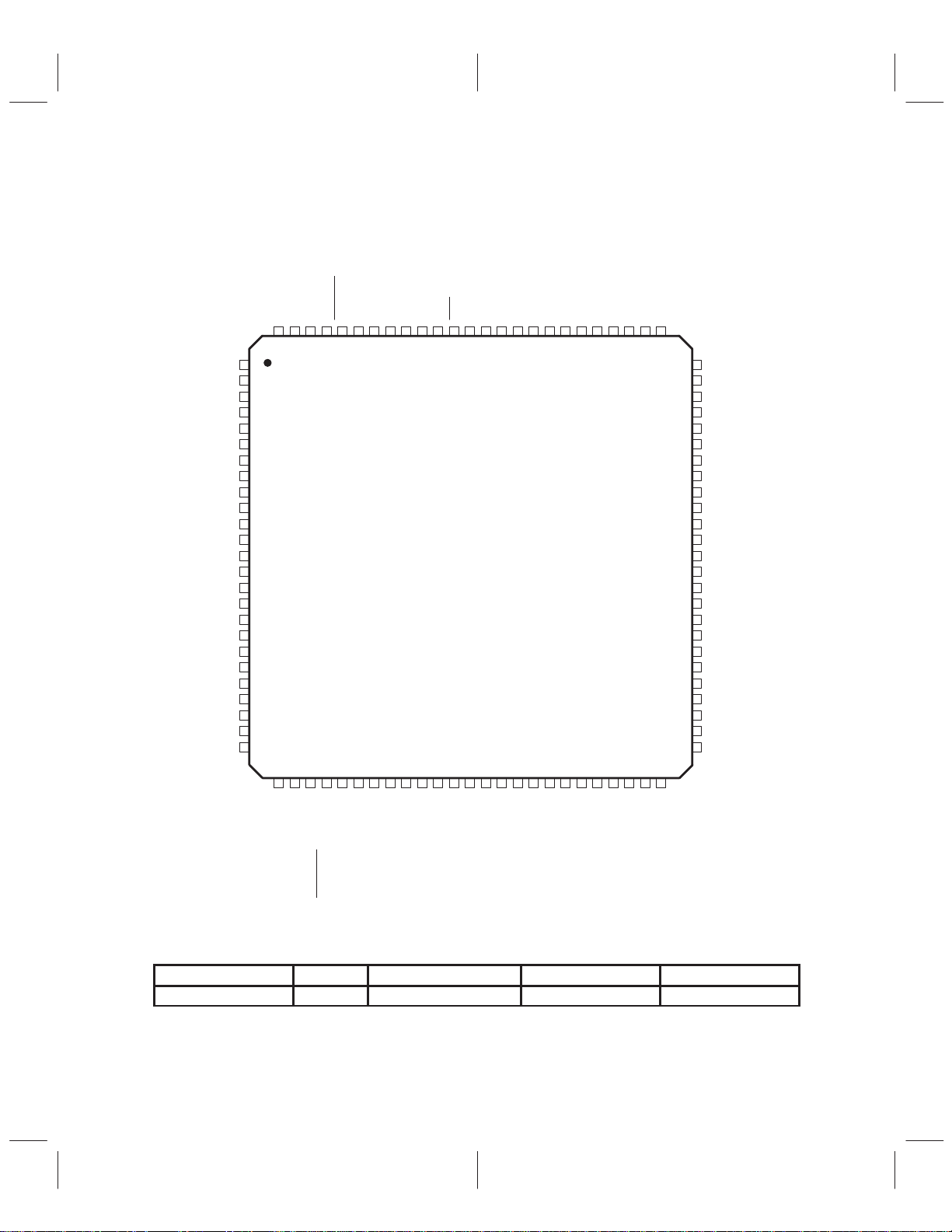
1.3 DVLynx Pinout
BDIF2
BDIF1
99
100
CC
+5V
CC
NC
1
2
3
4
5
6
7
8
9
10
11
12
13
14
15
16
17
18
19
20
21
22
23
24
25
26
27
BDI/O0
BDI/O1
BDI/O2
BDI/O3
V
BDI/O4
BDI/O5
BDI/O6
BDI/O7
GND
CNTNDR
TEST1
TEST2
TEST3
V
CC
BDOCLK
V
BDO0
BDO1
BDO2
BDO3
GND
BDO4
BDO5
BDIF0
GND
97
98
29
28
RESET
BDO_FR
BDI_FR
94
95
96
32
31
30
BDIEN
LPS (STAT0)
92
93
34
33
PZ PACKAGE
(TOP VIEW)
+5V
CC
INT
BDICLK
91
35
RDY
V
88
89
90
TSB12LV42
38
37
36
GND
86
87
40
39
CS1
MCSEL1
85
41
MCSEL0
MCCTL1
MCCTL0
82
83
84
44
43
42
CC
V
81
45
DATA0
80
46
DATA8
79
47
DATA1
DATA9
DATA2
76
77
78
48
49
50
75
74
73
72
71
70
69
68
67
66
65
64
63
62
61
60
59
58
57
56
55
54
53
52
51
DATA10
DATA3
DATA11
GND
DATA4
DATA12
DATA5
DATA13
V
CC
BCLK
+5V
V
CC
DATA6
DATA14
DATA7
DATA15
GND
ADR8
ADR7
V
CC
ADR6
ADR5
ADR4
ADR3
ADR2
ADR1
D3D1D0
BDO6
BDO7
TEST4
CC
V
CYCLEIN
GND
D2
CTL1
CTL0
+5V
CC
V
CC
V
SCLK
LREQ
BDOF0
GND
BDOF2
BDOF1
ADR0
BDOEN
ISOLAT (STAT1)
BDIBUSY (STAT3)
BDOAVAIL (STAT2)
1.4 Ordering Information
ORDERING NUMBER NAME VOLTAGE DATA RATE PACKAGE
TSB12LV42PZ DVLynx 3.3 V – 5 V Tolerant I/O’s Up to 200 Mbits/s 100 pin PQFP
1–3
Page 18

1.5 TSB12LV42 Terminal Functions
I/O
DESCRIPTION
TERMINAL
NAME NO.
ADR0 – ADR8 50, 51, 52,
53 54, 55,
56, 58 59
BCLK 66 I Host bus clock
BDI_FR 94 I Frame pulse input. The frame pulse input signal for PAL is 25 Hz and for
BDIBUSY(STAT3) 31 O BDIF is busy or status output 3. STAT3 is programmable at DIAG register
BDICLK 91 I Bulky data I/O clock. This terminal operates at up to 40 MHz.
BDIEN 93 I BDIO bus enable. If BDIEN is low, accesses to BDIO-bus are ignored.
BDIF2 – BDIF0 100, 99,
98
BDIO7 – BDIO0 9, 8, 7, 6,
4, 3 2, 1
BDO_FR 95 O Frame pulse output.
BDO7 – BDO0 27, 26, 25,
24 22, 21,
20, 19
BDOAVAIL(STAT2) 30 O Bulky data output available or status output 2. STAT2 is programmable at
BDOCLK 16 I Bulky data output clock. The bulky data output clock operates at up to
BDOEN 49 I BDO bus enable. If BDOEN is low, accesses to BDO-bus are ignored.
BDOF2 – BDOF0 47, 46, 45 O BDIF format bus for BDO Port. BDOF2 is the MSB.
CNTNDR 11 I/O Contender . The CNTNDR tells the Link when the local node is a contender
CS1 86 I Chip select. CS1 needs to be low when the device is to be selected for reads
CTL0, CTL1 40, 39 I/O Control 0 and control 1 of the Phy-Link control bus. CTL0 and CTL1 indicate
CYCLEIN 33 I Cycle In. CYCLEIN is an optional external 8-kHz clock used as the cycle
D0 – D3 38, 37, 36,35I/O Data 0 – 3 of the Phy-Link data bus. Data is expected on D0 – D1 for 100
DATA0 – DATA15 80, 78, 76,
74 71, 69,
64, 62 79,
77, 75, 73
70, 68, 63,
61
I MP/MC address lines. ADR0 is the MSB.
NTSC is 29.97 Hz at 50% duty cycle.
(reg 30h).
I/O BDIF format bus for BDIO port. BDIF2 is MSB.
I/O BDIF I/O data lines. BDIO7 – BDIO0 are high-speed I/O data lines for the
BDIF bus. They are primarily used for audio/data/video applications. These
lines can also be configured for input only. BDIO7 is the MSB.
O BDIF output data lines. BDO7 – BDO0 are data lines for high-speed output
on the BDIF bus for audio/data/video applications. These lines are
compliant with several standard interfaces. BDO7 is the MSB.
DIAG register (reg 30h).
40 MHz.
for IRM. This terminal can also be driven by the Link. The default status of
this terminal is input.
and writes.
the four operations that can occur in this interface.
clock. It should only be used when attached to the cycle master node. It is
enabled by the cycle source bit and should be tied high when not used.
Mbits/s and D0 – D3 for 200 Mbits/s. Data0 is the MSB.
I/O Data 0 – 15 of MC/MP host processor. Some of the DATAx terminals have
second functions depending on the status of the MCSEL terminals. DATA0
is the MSB.
1–4
Page 19
1.5 TSB12LV42 Terminal Functions (Continued)
I/O
DESCRIPTION
TERMINAL
NAME NO.
GND 10, 23, 34, 48
INT 89 O Interrupt. INT is used to notify the host that an interrupt has occurred.
ISOLAT(STAT1) 29 I/O Isolation or status output 1. ISOLA T is sampled during hardware reset to
LPS/STAT0 92 O Link power status or status output 0. LPS is used to drive the LPS input to
LREQ 44 O Link request. LREQ is a DVLynx output that makes bus request and
MCCTL0/1 82, 83 I Control lines for bus access. MCCTL0 and MCCTL1 function depends
MCSEL0/1 84, 85 I Select lines for MP/MC. MCSEL0 and MCSEL1 are selection lines for
NC 18 O No connect
RDY 88 O Ready line. When high, RDY indicates the end of an MP/MC access.
RESET 96 I Reset (active low). RESET is the asynchronous power on reset to the
SCLK 42 I System clock. SCLK is a 49.152-MHz clock from the Phy. This terminal
TEST1 12 I Test pin should be tied to VCC.
TEST2 13 I Test should be tied to GND.
TEST3 14 I Test pin should be tied to VCC.
TEST4 28 I Test pin should be tied to GND.
V
CC
VCC5V 15, 41, 65, 90 5-V ±5% power supplies for 5V tolerant I/O terminals. These terminals
60, 72, 87, 97
5, 17, 32, 43
57, 67, 81
Ground
This terminal can be active low or active high depending on the status of
the INTPOL bit in IOCR register. It is high-impedance when no interrupt
is pending.
determine if isolation is present. When this terminal is high, this indicates
NO isolation is being used. STA T1 is driven as an output after hardware
reset and used as a status output. STAT1 is programmable in the DIAG
register (reg 30h)
the Phy. This signal indicates that the LLC is powered up and active. This
output toggles at 1/32 of BCLK or SYSCLK depending on the
microprocessor used. STA T0 is used to MUX out internal signals. ST AT0
is programmable in the DIAG register (reg 30h).
accesses the Phy layer.
on MP/MC type being used.
the MP/MC-type being used. These terminals have an impact on the
function MCTRL,ADR, RDY and DA TA terminals.
device.
generates the 24.576-MHz clock (NCLK).
3.3 V (3 V – 3.6 V) supply voltage
can be tied to 3.3 V if no 5 V devices interface to the TSB12LV42.
1–5
Page 20

1–6
Page 21
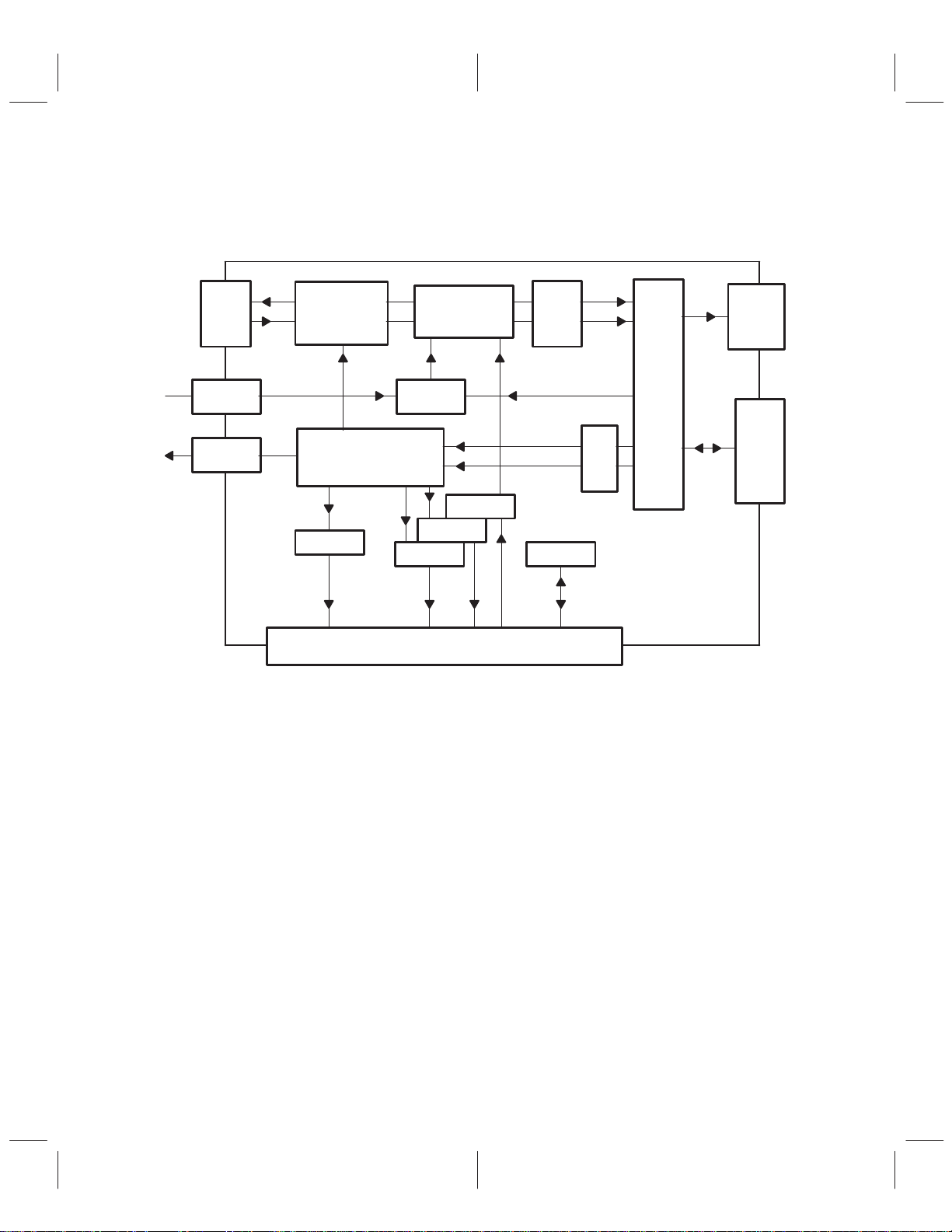
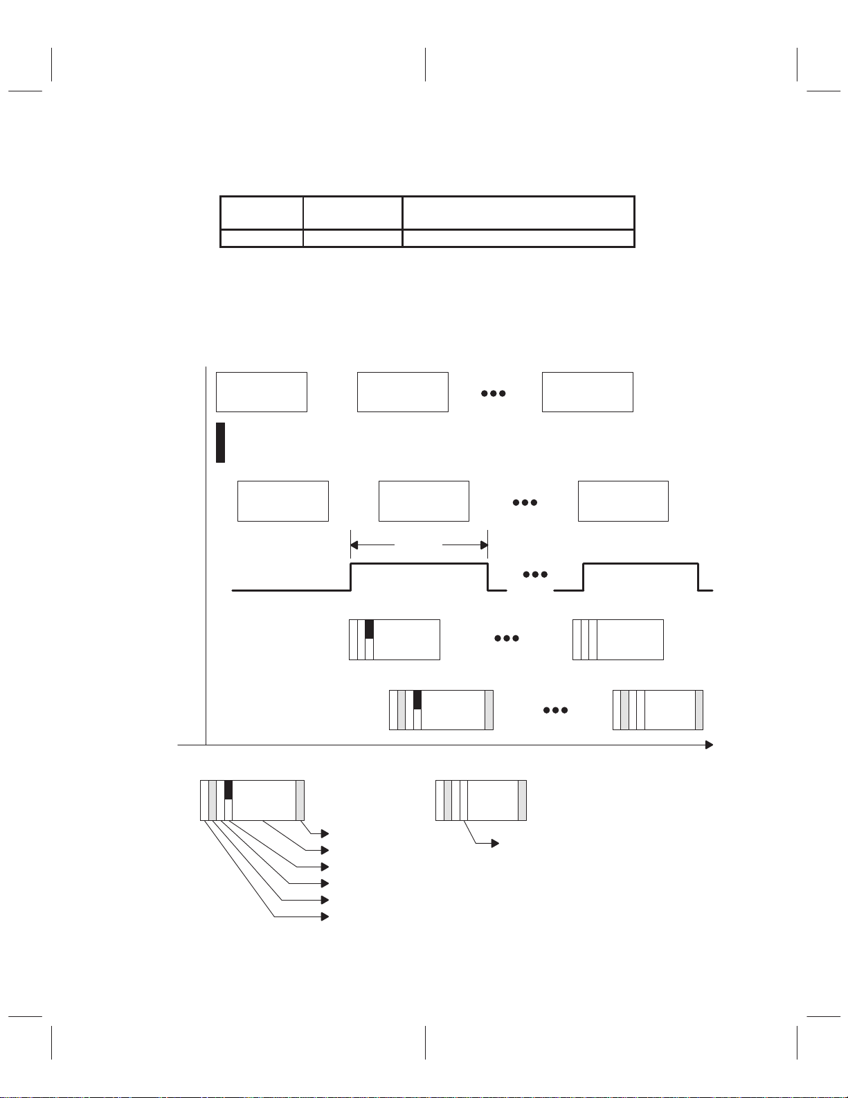
2 Architecture
BDIF
8K Byte
6-Queue
Bulky FIFO
DV/A/I
Packetizer
FrP In TS Gen
Rx/Router/
FrP Out
Time Stamp
Recovery
ATF
BusRST
BRF
ARF
MC/MP Interface
Conventions:
Asynchronous packet = Async packet
Isochronous packet = Isoc packet
Asynchronous Transmit FIFO = ATF
Broadcast Receive FIFO = BRF
Asynchronous Receive FIFO = ARF
Configuration registers = CFR
SD-DVCR 480 byte source packet = DV-packet
MP/MC = Microprocessor/Microcontroller
Tx
CFR
Rx
Link
Core
CM/
CT
Status
Pins
PhyLink
IF
Figure 2–1. Functional Block Diagram
2.1 Bulky Data Interface
The bulky data interface (BDIF) enables the TSB12L V42 to provide sustained data rates up to 160 Mbits/s.
The bulky data FIFO supports DV compressed data as defined by the Blue Book standard for digital video,
asynchronous, and isochronous data for both transmit and receive.
2.2 Bulky Data FIFO
The bulky data FIFO is where the BDIF buffers the transmit or receive data. The bulky data FIFO is
partitioned into six logical divisions. Each of these logical FIFO sizes are programmable on four quadlet
boundaries. These six FIFOs are:
• Bulky DV transmit FIFO (BDTX)
• Bulky DV receive FIFO (BDRX)
• Bulky asynchronous transmit FIFO (BATX)
2–1
Page 22

• Bulky asynchronous receive FIFO (BARX)
• Bulky isochronous transmit FIFO (BITX)
• Bulky isochronous receive FIFO (BIRX)
The following sections give functional descriptions to these logical FIFOs. See Section 4.1,
Interface
, for more detail on using this FIFO to transmit/receive data.
Bulky Data
2.2.1 Bulky DV Transmit FIFO (BDTX)
The BDTX FIFO is used to transmit DV data according to the Blue Book standard. Data is typically written
to this FIFO for the BDIF or microcontroller interface in quadlets (four bytes). The TSB12LV42 can be
configured to automatically insert 1394 isochronous headers, CIP (or common isochronous packet)
headers, and H0 DIF blocks. The TSB12L V42 can also be configured to automatically insert empty packets
to smooth out the bursty data rates. This is necessary to accommodate receiving nodes whose FIFO’s are
sized to receive evenly distributed data.
2.2.2 Bulky DV Receive FIFO (BDRX)
The BDRX FIFO is typically used to store DV data received from the link layer core and then forward it on
to a high speed application via the BDIF . Only isochronous port 0 of the link layer core can access the BDRX
FIFO.
2.2.3 Bulky Asynchronous Transmit FIFO (BATX)
The BATX FIFO is typically used to transmit asynchronous data packets from high-speed applications.
Either the BDI or the microcontroller can load data into this FIFO.
2.2.4 Bulky Asynchronous Receive FIFO (BARX)
The BARX FIFO is typically used to store received asynchronous data packets to be forwarded to a
high-speed application via the BDIF. The microcontroller can also read data from the BARX FIFO one
quadlet at a time. This FIFO is the default location for self-IDs.
2.2.5 Bulky Isochronous Transmit FIFO (BITX)
The BITX FIFO is typically used to transmit isochronous data packets from high-speed applications. Data
can be loaded into the FIFO by either the BDIF or by the microcontroller one quadlet at a time.
2.2.6 Bulky Isochronous Receive FIFO (BIRX)
The BIRX FIFO is typically used for receiving isochronous data and forwarding it to a high-speed application
via the BDIF . Data can also be forwarded to the microcontroller interface one quadlet at a time. Isochronous
ports 1 through 7 have access to this FIFO. Each port can be programmed to filter incoming packets
according to the isochronous channel and/or isochronous header T AG value.
2.3 DV Transmit and Receive Control
The DVLynx transmit and receive circuitry controls automatic insertion of the common isochronous packet
(CIP) header information as defined by the IEC 61883 standard. This circuitry also controls the automatic
insertion of the H0 DIF block header as defined by the Blue Book standard for SD-DVCR. The transmit
circuitry also includes automatic timestamp insertion. The TSB12LV42 has an empty packet insertion
function that will automatically insert a number of empty packets within a frame. These empty packets
smooth out bursty data so that it is easier to handle for the receiving node, whose FIFOs are designed for
evenly distributed data.
2–2
Page 23

2.4 Microprocessor/Microcontroller Interface
The microprocessor/microcontroller interface (MP/MC) is used as the host controller port. It is designed to
work with several standard MP/MCs including Motorola 68000, Intel 8051, and ARM processors. The
interface supports both 8-bit and 16-bit wide data busses as well as both little endian and big endian
microcontrollers. This interface has two basic modes of operation: handshake Mode and blind access mode.
See Section 4.2,
Microprocessor Interface
, for more details.
2.5 Control FIFO
The control FIFO is partitioned into three logical FIFOs. The size of each of these logical FIFOs is
programmable on quadlet boundaries. These three FIFOs are called:
• Asynchronous control transmit FIFO (ACTX)
• Asynchronous control receive FIFO (ACRX)
• Broadcast write receive FIFO (BWRX)
2.5.1 Asynchronous Control Transmit FIFO (ACTX)
The ACTX FIFO is typically used to transmit small asynchronous control packets sent by the
microprocessor/microcontroller. The ACTX FIFO can also be used to support asynchronous traffic at very
low data rates. Asynchronous packets are written into the FIFO and transmitted using the ACRXF , ACTXC,
and ACTXCU registers. See Section 3.3.1,
concerning the ACTX.
Transmitting Asynchronous Control Packets
2.5.2 Asynchronous Control Receive FIFO (ACRX)
The ACRX FIFO is typically used to receive asynchronous control packets other than self-ID packets.
Regular asynchronous control packets are usually received to the ACRX FIFO. This FIFO is accessible by
the microcontroller port through the ACRX register. See Section 3.4.1,
for more details concerning the ACRX.
Receiving Asynchronous Packets
, for more details
,
2.5.3 Broadcast Write Receive FIFO (BWRX)
The BWRX FIFO is typically used to receive asynchronous broadcast write request packets. See
Section 3.4.1,
Receiving Asynchronous Packets
, for more detail concerning the BWRX.
2.6 Physical Layer
The physical layer interface provides phy-level services to the transmitter and receiver. This includes
gaining access to the serial bus, sending packets, receiving packets, and sending/receiving acknowledges.
The TSB12LV42 supports Texas Instruments bus-holder circuitry on the Phy-link interface terminals. By
using the internal bus holders, the user avoids the need for the complex Annex J isolation method. The bus
holders are enabled by connecting the ISOLA T
terminal to ground.
2.7 Configuration Register (CFR)
The TSB12L V42 is configured for various modes of operation using CFRs. These registers are accessed
via the host microprocessor/microcontroller. The CFR space is 512 bytes, thus the need for a 9-bit address
bus. All CFRs are 32-bits wide. Since the microcontroller interface is either 8 or 16-bits wide, it must perform
a byte stacking/unstacking operation internally on the incoming (write) or outgoing (read) microcontroller
data. Chapter 5 gives a map of all the registers and detailed descriptions of all the register bits.
2–3
Page 24

2–4
Page 25

3 Functional Description and Data Formats
3.1 Overview
The TSB12L V42 is a 1394 interface for high-speed audio, video, and data applications at up to 200 Mb/s.
For these high-speed applications a bulky data interface (BDIF) has been implemented that supports long
term data rates up to 60 Mb/s. Burst data rates, however, can go up to 160 Mb/s.
The TSB12L V42 contains two FIFOs that are a 256-byte control FIFO (Control FIFO) and an 8K-byte BDIF
FIFO. These two FIFOs are further subdivided into smaller logical FIFOs.
Bulky data is usually buffered in the BDIF FIFO. The BDIF FIFO supports DV, asynchronous, and
isochronous formatted traffic for receive and transmit.
Asynchronous packets (for 1394 bus control/status) are usually written to or read from the Control FIFO.
For lower data rates the Control FIFO can also be used to buffer asynchronous application data. Based on
destination address, received asynchronous request packets may be steered into either the Control FIFO
or the BDIF FIFO.
A separate self-ID-FIFO allows faster BUS setup and reduces software complexity . The 256-Byte Control
FIFO (Control FIFO) is partitioned into three logical FIFOs. The size of these three logical FIFOs is
programmable on quadlet boundaries. These FIFOs are called:
1. Asynchronous control transmit (ACTX) FIFO
2. Asynchronous control receive (ACRX) FIFO
3. Broadcast write receive (BWRX) FIFO.
The 8K-Byte BDIF FIFO is partitioned into six logical FIFOs. The size of these FIFOs is programmable on
four quadlet (hexlet) boundaries. These FIFOs are called:
1. BDIF DV transmit (BDTX) FIFO
2. BDIF DV receive (BDRX) FIFO
3. BDIF asynchronous transmit (BATX) FIFO
4. BDIF asynchronous receive (BARX) FIFO
5. BDIF isochronous transmit (BITX) FIFO
6. BDIF isochronous receive (BIRX ) FIFO
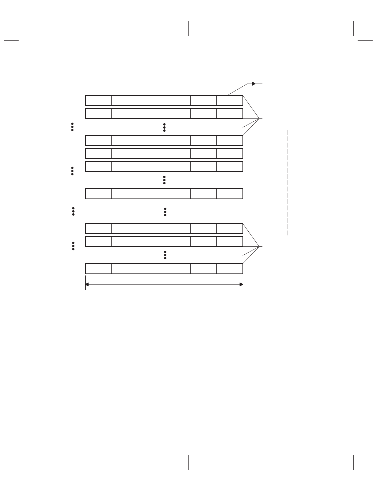
The Control and BDIF FIFOs are structured are as follows:
8K-Byte BDIF FIFO Structure
256-Byte Control
FIFO Structure
00h
FFh
ACTX
ACRX
BWRX
0000h
1FFFh
DV TX Buffer
DV RX Buffer
Async TX Buffer
Async RX Buffer
Isoch TX Buffer
Isoch RX Buffer
The TSB12L V42 (with built-in programmable Endianness) interfaces directly to most microprocessors and
microcontrollers.
3–1
Page 26
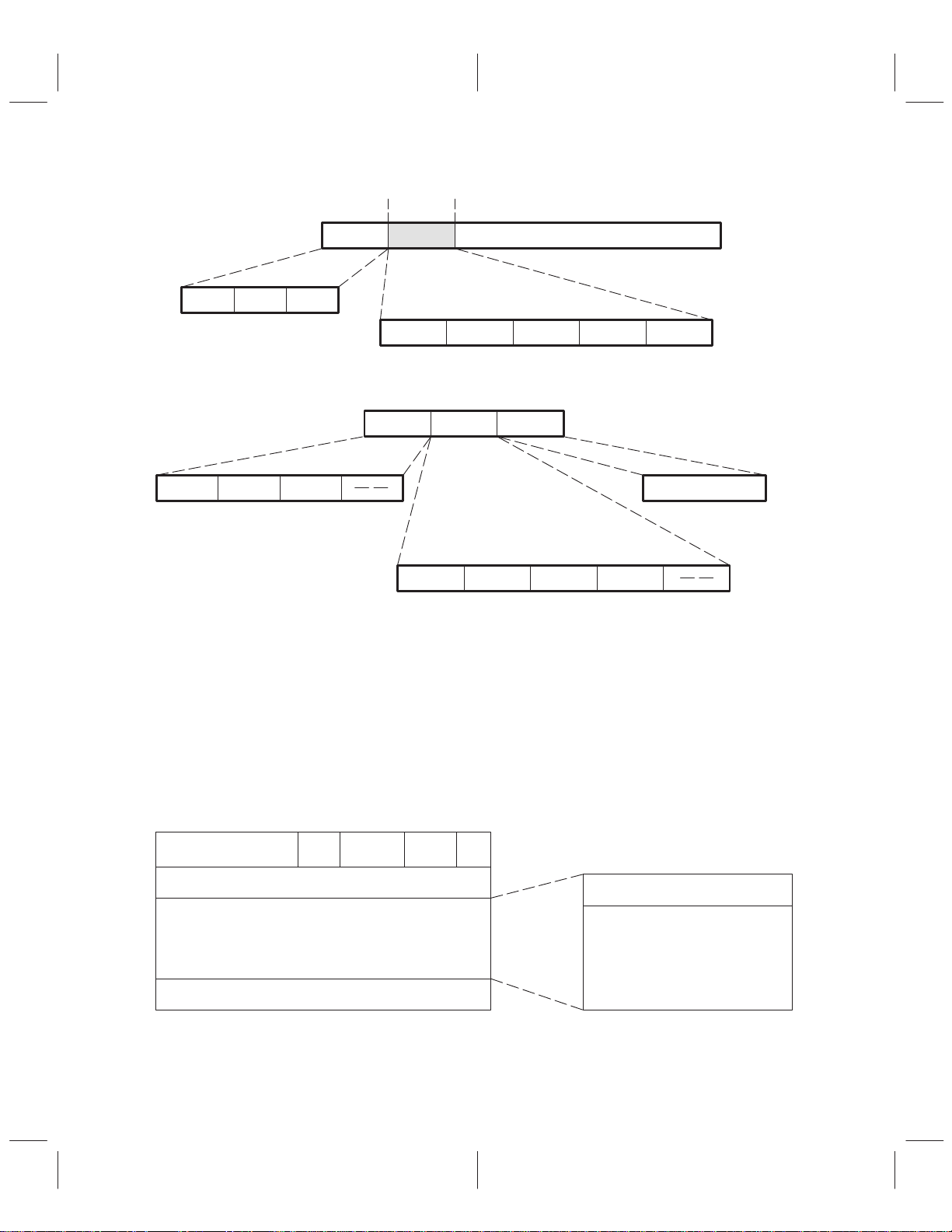
3.2 DV on 1394 Overview
3.2.1 DV interface
NCLK
820020 Clocks
250 Source Packets NTSC
BDI_Fr
NTSC PAL
3280 Clks for 249 SPs
3300 Clks for Last SP
983040 Clocks
300 Source Packets PAL
3277 Clks for 299 SPs
3217 Clks for Last SP
Figure 3–1. Example of a Source Packet Transmit Event
A source packet (SP) event occurs 250 times in 1 NTSC frame or 300 times in 1 PAL frame. NCLK is an
internal 24.576-MHz clock derived from the 49.152-MHz SCLK. The first BDI_FR pulse starts the source
packet counter used to generate the empty packet insertion algorithm. The TSB12L V42 provides automatic
empty packet insertion on transmit to evenly distribute the 250/300 source packets within a frame. Turning
off the appropriate bit in the MDCR Register can turn off this feature. In one NTSC frame, there are 820020.0
NCLKs and therefore 3280.08 NCLKs per source packet. That is equivalent to 249 source packets of 3280
NCLKs and one source packet of 3300 NCLKs. For NTSC a SP event is signaled every 3280 clocks for the
first 249 SP event and the last SP event is signaled after 3300 clocks following the 249th event. This yields
a 33.367-ms frame rate (40.69 ((3280 × 249) + 3300)). For PAL the time for 1 frame is 40.00 ms
(40.69 ((3277 × 299) + 3217)).
Cycle synchronous (CS) events occurs every 125 µs ( this is the isochronous cycle base rate). During each
isochronous cycle a complete SP is transmitted or an empty packet (EP) is transmitted. If two contiguous
CS events occur without an SP event occurring, then an empty packet is forced in the current isochronous
cycle regardless if a complete source packet is available in the FIFO. If a SP event occurs between two CS
events but a complete source packet is not available in the FIFO, then an empty packet is transmitted in the
current isochronous cycle.
NCLK
BDI_Fr
CLK_cntr
SPevent
Valid
001 002 3280 001 002 3300 001 002
Figure 3–2. Source Packet Transmit Event Timing
NOTE: BDI_Fr has already been synchronized with NCLK.
3–2
Page 27
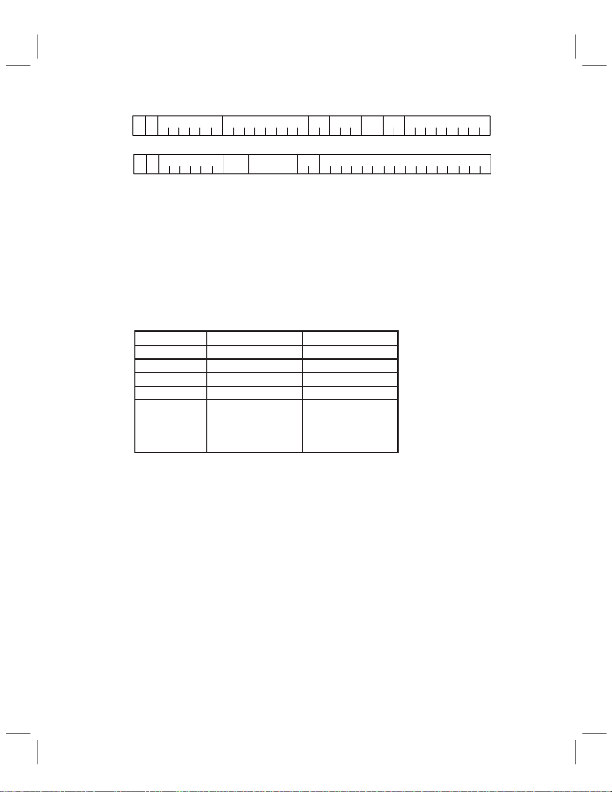
3.2.2 DV Bandwidth on IEEE1394
Table 3–1. DV Bandwidth on IEEE 1394
MAX SP-BW
(Mbits/s)
30.72 32 20/500
†
SP-BW: Source package bandwidth (based on 480 byte DV).
‡
1394-BW: Overall bandwidth of 1394 bus on physical medium (includes 4-byte 1394
packet transmit header, 4-byte packet header CRC, 8-byte CIP header, actual
payload, and 4-byte payload CRC. This bandwidth should be allocated by the DV
transfer initiator.
†
MAX 1394-BW
(Mbits/s)
‡
3.2.3 DV Transmission over IEEE1394
A DV-packet on the 1394 bus:
POSSIBLE DV BUS PACKET SIZE IN-
CLUDING CIP, 1394-Hdr, CRCs (Bytes)
Data from
DV Appl.
Data from
TS Gen.
Input to
Transmitter
Internal
I-slot
Enable
Data to
Linkcore
Data on
1394 Bus
A DV-packet on the 1394 bus:
1st DV-cell
480 Bytes
480 Bytes
2nd DV-cell
125 µs
492 Bytes
500 Bytes
250/300th
DV-cell
Time
Payload CRC
DV-cell
CIP1 with timestamp
CIP0 Header
Header CRC
1394 Header
CIP1 without timestamp
Figure 3–3. DV Packet on 1394 Bus
3–3
Page 28
3.2.4 Source Packet/DIF Block Format
Source
Packets
80 Bytes DIF Block
0
1
24
25
49
225
249
H0 SC0 SC1 VA0 VA1 VA2
A0 V0 V1 V2 V3 V4
V129 V130 V131 V132 V133 V134
H0 SC0 SC1 VA0 VA1 VA2
A0 V0 V1 V2 V3 V4
V129 V130 V131 V132 V133 V134
H0 SC0 SC1 VA0 VA1 VA2
A0 V0 V1 V2 V3 V4
V129 V130 V131 V132 V133 V134
DIF Sequence 0
DIF Sequence 9
480 Bytes (120 Quadlets) Data Block
NOTES: A. SD-DVCR 525-50 System is identical to 525-60 system except the number of source packets is 300
B. H0 = Header DIF block
SCi = Subcode DIF block (i = 0, 1)
VAi = VAUX DIF block i (i = 0, 1, 2)
Vi = Video DIF block (i = 0 – 134)
Ai = Audio DIF block (i = 0 – 8)
Figure 3–4. DIF Block H0
The H0 DIF block is inserted into the first 80 bytes every 25th packet. The TSB12LV42 gives the system
designer the option to automatically insert the 80 byte DIF block before transmit. The value of the H0 header
DIF block is programmable via internal registers 1A4h and 1A8h.
Figure 3–5 shows the H0 header DIF block. Bytes 0–7 can be inserted by the link core or can be provided
by the application with the data.
3–4
Page 29
ID0 ID1 ID2
Byte Position
0 1 2 8 . . . . .. . . . . . . . . . . . . . . . . . . . . . . . . . 793 7
ID FF_FF_FF_ . . . . . . . . . . . . . . _FFH0
H0R3 H0R4 H0R5 H0R6 H0R7
Figure 3–5. ID Data In DIF Block
ID0
SCT2 SCT1 SCT0
MSB
MSB
ID1 ID2
DBN7 . . . DBN0
DSEQ3 DSEQ2 DSEQ1 DSEQ0
Figure 3–6. ID Data in DIF Block
3.2.5 DV Packets CIP Header Calculations
The TSB12LV42 has an option to automatically insert CIP headers and timestamps during transmission.
The CIP headers, or common isochronous packet headers, follow the format of the IEC 61883-2 standard
for transmitting SD-DVCR data over 1394. The values of the CIP headers are programmable in registers
1CCh and 1D0h. The TSB12L V42 also has the option to automatically calculate and insert timestamp values
into the CIP1 header. The timestamp is inserted either into the first transmitted packet in the next
isochronous cycle (register F0h, bit 1 1 INTSSP=0) or into the first full data packet of the next frame (register
F0h, bit 1 1 INTSSP=1).
Data_Length
T ag Channel Tcode Sy
Header_CRC
Data Field
Data_CRC
Length field is either 488 bytes (DV-Source Packet) or 8 bytes (empty packet).
Figure 3–7. DV Source Packet Format
CIP Header
Real Time Data
3–5
Page 30
DCIP0 00
SID
DBS FN QPC rsv DBC
SPH
DCIP1 01
static values:
DXH: tag,chanNum, spd, sy (1394 Isochronous Header)
DCIPX0:SID, DBS, FN, QPC, SPH, DBC
DCIPX1:FMT, 50/60, STYPE
calculated values:
DXH: length (1394 Isochronous Header)
DCIPX1: SYT
DCIPX0: DBC
STYPE 50/60 50/60
00000 525–60 System
00001 Reserved Reserved
00010 1125–60 System 1250–50 System
0001 1
11111
†
525-60 system: The 525-line system with a frame frequency of 29.97 Hz
625-50 system: The 625-line system with a frame frequency of 25.00 Hz
SD-DVCR: Standard-definition digital-video cassette recorder
FMT
50/60
STYPE
rsv SYT
Figure 3–8. CIP Header Format
0 1
†
.
.
.
Reserved Reserved
625–50 System
†
3.3 Transmit Operation
The functional description for transmission is shown in the following sections. The transmit format describes
the expected organization of data presented to the TSB12L V42 at the host-bus interface.
3.3.1 Transmitting Asynchronous Control Packets
Asynchronous control packets are typically transmitted by the microprocessor (host) using the
Asynchronous Control Transmit FIFO (ACTX). This FIFO is part of the 256 bytes Control FIFO. It is
configurable in register 44h (Asynchronous Control Data Transmit FIFO Status). The ACTX FIFO can also
be used for asynchronous data traffic at low data rates.
For transmit, the 1394 asynchronous headers and the data are loaded into the ACTX by the microprocessor.
The microprocessor has access to the ACTX FIFO through registers 80h – 8Ch. The asynchronous header
must fit the format described in Section 3.6,
TSB12LV42)
3–6
.
Asynchronous Transmit Data Formats (Host Bus to
Page 31

Bulky Data FIFO
BD–IF
Control FIFO
CFR
MPMC–IF
Header, Data
Phy–IF
Figure 3–9. Transmit from the Asynchronous Control Transmit FIFO (ACTX)
To transmit an asynchronous packet from the ACTX:
• Register 80h (asynchronous cControl data transmit FIFO first): The first quadlet of an
asynchronous packet is written to this register by the application software for transmit.
• Register 84h (asynchronous control data transmit FIFO continue): All remaining quadlets of an
asynchronous packet except the last are written to this register by the application software for
transmit.
• Register 8Ch (asynchronous control data transmit FIFO last and send): The last quadlet of an
asynchronous packet is written to this register by the application software. Once the last quadlet
is written into the ACTX FIFO using this register, the entire packet is transmitted.
NOTE:
Register 88h (asynchronous control data transmit FIFO first and update) can be
used in conjunction with register 8Ch (asynchronous control data transmit FIFO
last and send) as an alternative method for transmitting asynchronous control
packets from ACTX. The first quadlet and all continuing quadlets except the last
are written to register 88h one quadlet at a time. Each quadlet is transmitted
immediately. The last quadlet is written to register 8Ch and also transmitted
immediately. This method of transmit should only be used in systems where the
microprocessor can keep up with the 1394 bus speed.
3.3.2 Transmitting Asynchronous Data Packets
Asynchronous data packets are typically transmitted from the bulky asynchronous transmit FIFO (BATX)
using either the bulky data interface (BDIF) or the microprocessor/microcontroller interface (MP/MC IF). The
BATX size is configurable in multiples of four quadlets in register 104h (bulky asynchronous size register).
The number of empty quadlet locations available in the BATX is provided in register 108h (bulky
asynchronous available register). The transmit operation for the BA TX FIFO is configurable in register ECh
(asynchronous/isochronous application data control register).
The BATX has an auto-packetization feature. This allows the user to program header registers within the
DVLynx CFRs and supply raw data to the DVLynx for transmit. The DVLynx automatically inserts the
appropriate 1394 headers for transmit. The asynchronous packet is transmitted once the last byte is
indicated on bulky data interface or microprocessor interface. If the number of quadlets in the FIFO is not
a multiple of 4, then some byte padding is performed (see Section 3.3.4,
Byte Padding
). These headers for
3–7
Page 32

auto-packetization are available in registers 1B0 – 1BCh. Please note that the headers programmed in
registers 1B0 – 1BCh for auto packetization must match the formats described in Section 3.6,
Transmit Data Formats (Host Bus to TSB12LV42)
. The DVLynx uses the information from these header
Asynchronous
registers to create the 1394 asynchronous headers. Please note that automatic header insertion is only
supported for write request operations (tcode 0 and 1). If the number of bytes in the transmitted packet is
different from the datalength field in the header, then receiving node receives the packet with errors.
There are four methods of transmitting asynchronous data from the BATX. The control signals located in
register ECh that are necessary for these four modes are summarized in the following text. A detailed
description is included for each mode.
MODE ATENABLE BDAXE AHIM DATA SOURCE HEADER SOURCE
1 1 1 1 Bulky data interface Configuration registers
2 1 0 1 Microprocessor interface Configuration registers
3 1 1 0 Bulky data interface Bulky data interface
4 1 0 0 Microprocessor interface Microprocessor interface
Mode 1: Transmit Asynchronous Data from BATX Using The BDIF, Data Is
Auto-Packetized
The BDIF writes data to the BA TX. This data does not include any asynchronous header bytes. Registers
1B0 – 1BCh (AHEAD0 – AHEAD3) are programmed with the 1394 asynchronous header information. The
packet is transmitted once the last byte is written into the BA TX. The last byte is signaled by the Bulky Data
Interface format lines (BDIF[2..0]) (settings for register ECh in this mode: ATENABLE=1, BDAXE=1,
AHIM=1) (see Figure 3–10).
Data
Asynchronous,
Isochronous Tx
BD–IF
Bulky Data FIFO
Phy–IF
Headers
Control FIFO
Cycle Timer
CFR
MPMC–IF
Figure 3–10. Transmit Asynchronous/Isochronous Data from BATX
by the Bulky Data Interface with Auto-Packetization
Mode 2: Transmit Asynchronous Data from BATX Using the MP/MC IF, Data Is
Auto-Packetized
The MP/MC IF writes data to the BATX using registers 10Ch and 110h. This data does not include any
asynchronous header bytes. Registers 1B0 – 1BCh (AHEAD0 – AHEAD3) are programmed with the 1394
asynchronous header information. Register 10Ch (asynchronous application data transmit FIFO first and
continue) allows the MP/MC to write the all quadlets of the packet to be sent except for the last into the BA TX.
The last quadlet of the asynchronous packet is written into register 110h (asynchronous application data
transmit FIFO last and send). The data is transmitted once the last quadlet is written into register 110h
(settings for register ECh in this mode: ATENABLE=1, BDAXE=0, AHIM=1) (see Figure 3–11).
3–8
Page 33

Asynchronous,
Isochronous Tx
BD–IF
Cycle Timer
Bulky Data FIFO
Phy–IF
Headers
Control FIFO
CFR
MPMC–IF
Data
Figure 3–11. Transmit Asynchronous/Isochronous Data from BATX
by the MP/MC Interface with Auto-Packetization
Mode 3: Transmit Asynchronous Data from BATX Using the BDIF, Data Is Fully
Formatted from the Application
The BDIF writes data to the BA TX. This data includes all asynchronous header and data bytes. The header
quadlets must match the format as shown in Section 3.6,
to TSB12LV42)
. The packet is transmitted once the last byte is written into the BATX. The last byte is
signaled by the bulky data interface format lines (BDIF[2..0]) (settings for register ECh in this mode:
A TENABLE=1, BDAXE=1, AHIM=0) (see Figure 3–12).
Asynchronous T ransmit Data Formats (Host Bus
Headers
and Data
BD–IF
Cycle Timer
Bulky Data FIFO
Phy–IF
Control FIFO
CFR
MPMC–IF
Asynchronous,
Isochronous Tx
Figure 3–12. Transmit Asynchronous/Isochronous Data from BATX
by the Bulky Data Interface, No Auto-Packetization
3–9
Page 34

Mode 4: Transmit Asynchronous Data from BATX Using the MP/MC IF, Data Is Fully
Formatted from the Application
The MP/MC IF writes data to the BA TX using registers 10Ch and 1 10h. This data includes all asynchronous
header and data bytes. The header quadlets must match the format as shown in Section 3.6,
T ransmit Data Formats (Host Bus to TSB12L V42)
. Register 10Ch (asynchronous application data transmit
FIFO first and continue) allows the MP/MC to write the all quadlets of the packet to be sent except for the
last into the BA TX. The last quadlet of the asynchronous packet is written into register 1 10h (asynchronous
application data transmit FIFO last and send). The data is transmitted once the last quadlet is written into
register 1 10h (settings for register ECh in this mode: ATENABLE=1, BDAXE=0, AHIM=0) (see Figure 3–13).
Asynchronous
BD–IF
Cycle Timer
Bulky Data FIFO
CFR
MPMC–IF
Headers
and Data
Control FIFO
Phy–IF
Asynchronous,
Isochronous Tx
Figure 3–13. Transmit Asynchronous/Isochronous Data from BATX
by the MP/MC Interface, No Auto-Packetization
General Asynchronous Transmit Notes
• Packet llush: The entire BA TX FIFO can be flushed by setting the AXFLSH bit in register ECh.
• Packet retries: Bulky asynchronous packets may be automatically retried up to 256 times
(BATxRetryNum in register 14Ch, BARTRY) in up to 256 isochronous cycles (BATxRetryInt in
register 14Ch, BARTRY). Packet retries for the asynchronous control transmit FIFO are manual.
• Retry protocol: The DVLynx uses single phase retries only.
• Auto-packetization: For the bulky data interface, if the data from the host is a multiple of four
bytes, then there is no need to indicate last byte of an asynchronous packet to the bulky data
interface. Similarly , if data from the microprocessor interface is a multiple of four bytes, then all
of the data can be written to register 10Ch only. The packet is transmitted on the bus once the
number of bytes in the FIFO is equal to the data length field of the asynchronous header.
• Acknowledges received for an asynchronous packet transmitted from the bulky asynchronous
transmit FIFO (BATX) are available in register 08h (BA T ACK Register). Bit 23 indicates if the ack
received was normal, BATACK[23] = 0, or if it was an error, BATACK[23] = 1. BATACK[24:27]
gives the acknowledge error if one occurred.
3–10
Page 35

• Acknowledges received for an asynchronous packet transmitted from the asynchronous control
transmit FIFO (ACTX) are available in register 04h (CA TACK Register). Bit 23 indicates if the ack
received was normal, CA TACK[23] = 0, or if there was an error , CA TACK[23] = 1. CA T ACK[24:27]
gives the acknowledge error if one occurred.
3.3.3 Transmitting Isochronous Packets
Isochronous data is transmitted from the bulky isochronous transmit FIFO (BITX) using either the bulky data
interface (BDIF) or the microprocessor/microcontroller interface (MP/MC IF). The BITX size is configurable
in multiples of four quadlets in register 12Ch (bulky isochronous size register). The number of empty quadlet
locations available in the BITX is provided in register 130h (bulky isochronous available register). The
transmit operation for the BITX FIFO is configurable in register ECh (asynchronous/isochronous application
data control register).
The BITX has an auto-packetization feature which allows the user to program header registers within the
DVLynx CFRs. The application can then supply raw data to the DVLynx for transmit, and the DVLynx
automatically packetizes the data and insert the appropriate 1394 header for transmit. The amount of data
in the transmit FIFO should match the datalength field in the isochronous header. Some byte padding is
performed when the data does not end on a quadlet boundary. See Section 3.3.4,
Byte Padding
information on byte padding. If the number of bytes in the packet is different from the datalength field of the
header, then the receiving node receives the packet with errors. The 1394 isochronous header for
auto-packetization is available in registers 1C0h (Isochronous Header for Auto TX). The header
programmed in register 1C0h must match the format given in Section 3.7,
Receive Data Formats (Host Bus to TSB12LV42)
. The DVLynx uses the information from these registers
Isochronous Transmit and
to create the 1394 isochronous headers.
There are four methods of transmitting isochronous data from the BITX. The control signals located in
register ECh that are necessary for these four modes are summarized in the following text. A detailed
description is also included for each mode.
, for more
MODE ITENABLE BDIXE IHIM DATA SOURCE HEADER SOURCE
1 1 1 1 Bulky data interface Configuration registers
2 1 0 1 Microprocessor interface Configuration registers
3 1 1 0 Bulky data interface Bulky data interface
4 1 0 0 Microprocessor interface Microprocessor interface
Mode 1: Transmit isochronous data from BITX using the BDIF, data is auto-packetized
The BDIF writes data to the BITX. This data does not include any isochronous header bytes. Register 1C0h
(IHEAD0) is programmed with the 1394 isochronous header information. The packet is transmitted once
the last byte is written into the BITX. The last byte is signaled to the BITX by the bulky data interface format
lines (BDIF[2..0]). The amount of transmitted data in the FIFO should match the data length field in the
isochronous header. Some byte padding is performed if the packet does not end on a quadlet boundary (see
Figure 3–10) (settings for register ECh in this mode: ITENABLE=1, BDIXE=1, IHIM=1).
Mode 2: Transmit isochronous data from BITX using the MP/MC IF, data is
auto-packetized
The MP/MC IF writes data to the BITX using registers 134h and 138h. This data does not include the 1394
isochronous header bytes. Register 1C0h (IHEAD0) is programmed with the 1394 isochronous header
information. Register 134h (isochronous transmit FIFO first and continue) allows the MP/MC to write all the
quadlets of the packet to be sent except for the last into the BITX. The last quadlet of the isochronous packet
is written into register 138h (isochronous transmit FIFO last and send). The data is transmitted once the last
quadlet is written into register 138h (see Figure 3–1 1) (settings for register ECh in this mode: ITENABLE=1,
BDIXE=0, IHIM=1).
3–11
Page 36

Mode 3: Transmit isochronous data from BITX using the BDIF, data is fully formatted
from the application
The BDIF writes data to the BITX. This data includes all isochronous header and data bytes. The 1394
isochronous header is the same format as described in Section 3.7,
Formats (Host Bus to TSB12LV42)
last byte is signaled by the bulky data interface format lines (BDIF[2..0]) (settings for register ECh in this
mode: ITENABLE=1, BDIXE=1, IHIM=0).
. The packet is transmitted once the last byte is written into the BITX. The
Isochronous Transmit and Receive Data
Mode 4: Transmit isochronous data from BITX using the MP/MC IF, data is fully
formatted from the application
The MP/MC interface writes data to the BITX using registers 134h and 138h. This data includes all
isochronous header and data bytes. The isochronous header quadlet is the same format as described in
Section 3.7,
(Isochronous Transmit FIFO First and Continue) allows the MP/MC to write the all quadlets of the packet
to be sent except for the last into the BITX. The last quadlet of the isochronous packet is written into register
138h (isochronous transmit FIFO last and send). The data is transmitted once the last quadlet is written into
register 138h (see Figure 3–13) (settings for register ECh in this mode: ITENABLE=1, BDIXE=0, IHIM=0).
Isochronous Transmit and Receive Data Formats (Host Bus to TSB12LV42)
. Register 134h
General Isochronous Transmit Notes
• Packet flush: The entire BITX FIFO can be flushed by setting the IXFLSH bit in the register ECh
(AICR).
• Auto-packetization: For the bulky data interface, if the data from the host is a multiple of four
bytes, then there is no need to indicate
interface. Similarly , if data from the microprocessor interface is a multiple of four bytes, then all
of the data can be written to register 134h only. The packet is transmitted on the bus once the
number of bytes in the FIFO is equal to the data length field of the isochronous header.
• The DVLynx can transmit more than one isochronous packet per isochronous cycle if the
application provides the 1394 isochronous header with the data and bit 24 of the isochronous
header is set to 1. The DVLynx arbitrates for the bus after every packet that is sent. No
concatenated isochronous subactions are allowed.
last byte
of an isochronous packet to the bulky data
3.3.4 Byte Padding
All packets on 1394 must end on a quadlet boundary (4 byte boundary). The DVLynx can insert padding
bits to a data packet that is not quadlet aligned. The DVLynx only adds padding bits to the last quadlet. This
allows for transmission of the data without any modification from the host. For isochronous data that is not
a multiple of four bytes, or does not end on a quadlet boundary , the BDIF format lines (BDIF[2–0]) indicate
the last byte of the packet. The bulky data interface logic adds padding zeroes to the data to insure that it
ends on a quadlet boundary .
3.3.5 Transmitting DV Formatted Isochronous Packets
Naming convention:
480 bytes = 120 quadlets
120 quadlets = 1 source packet = 1 data block
250 source packets = 1 frame for NTSC
300 source packets = 1 frame for PAL
DV data may be transmitted via the bulky data FIFO or the microcrontoller interface. The bulky data FIFO
DV transmit modes of operation are shown below. The following modes are supported; headers and data
from BDIF/micro, data from BDIF/micro, and headers from CFRs. In addition, DV transmit gives the option
of automatic timestamping, empty packet insertion, and inserting H0 DIF blocks. Most DV transmit functions
are controlled by the DCR register at address F0h.
If the BDDXE bit (DCR register) is set to logic 1, then the BDIF has access to the BDTX-FIFO. DV source
packets (SP) are usually transmitted via the bulky data interface. Here the single bytes are packetized into
3–12
Page 37

quadlets (1 quadlet = 4 bytes of data = 32 bits). After four bytes or 1 quadlet is written to the BDIF, the
complete quadlet is written to the bulky data DV transmit FIFO (BDTX). The first byte of a DV source packet
is indicated by setting the BDIF[2..0] signals to 101b. An internal cyclic counter keeps track of DV SP
boundaries. DV SP, frame size, and DIF blocks are shown in Section 3.2,
DV on 1394 Overview
.
If the BDDXE bit is set low, MC interface has access to the BDTX FIFO. Quadlets are written into the BDTX
FIFO through registers 160h and 164h.
The DHIM bit (DCR Register) selects if the 1394 header registers should be interleaved automatically
(DHIM=1) or if complete formatted DV source packet and 1394 headers are expected from the application
data source (DHIM=0) (see Table 3–2).
The H0INST bit (DCR register) selects if the H0 DIF block is automatically inserted by DVLynx (H0INST=1)
or if the H0 DIF block is supplied by the application (H0INST=0). If the H0INST bit is 1, indicating automatic
insertion of the H0 DIF block, the hardware still expects 480 bytes input for each source packet. See
Table 3–2.
T able 3–2. DHIM/H0INST Settings for Different Header Insertion Schemes
MODE BDDXE DHIM H0INST
1 1 1 1 Cycle timer CFR (internal) BDIF CFR (internal)
2 1 1 0 Cycle timer CFR (internal) BDIF BDIF
3 1 0 1 BDIF BDIF BDIF CFR (internal)
4 1 0 0 BDIF BDIF BDIF BDIF
5 0 1 1 Cycle timer CFR (internal) MP/MC CFR (internal)
6 0 1 0 Cycle timer CFR (internal) MP/MC MP/MC
7 0 0 1 MP/MC MP/MC MP/MC CFR (internal)
8 0 0 0 MP/MC MP/MC MP/MC MP/MC
TIME STAMP
FROM
HEADERS FROM DATA FROM DIF H0 FROM
On each isochronous transmission cycle the DV framer checks if 480 valid bytes are available in the BDTX
FIFO. If so, these bytes are appended with 8 bytes of CIP header information (if DHIM=1), taken as the
payload for a DV packet and sent over the 1394 bus. If 480 valid bytes are not available in the BDTX FIFO,
an empty DV packet is sent. Possible 1394 bus packet sizes are 500 bytes for a complete packet and 20
bytes for an empty packet.
A 20 quadlet DIF block (H0) is automatically inserted every 26 source packets of a DV frame. A total of 250
source packets make up a DV frame for NTSC and, 120 quadlets make up a source packet. These DIF
blocks are numbered in a sequence, 0 through 9. The first DIF block, DIF Sequence 0, contains header
information, subcode, audio and video data. The following DIF blocks in the sequence contain similar
information. However, DIF Sequence 9 also indicates the end of a frame.
Mode 1: Data from bulky data interface, headers/timestamp/H0 automatically inserted
The application provides a 480 byte data packet to the Bulky Data Interface. The DVLynx automatically
formats the packet and transmits it over 1394. The DVLynx only transmits a packet if there are 480 bytes
of data available in the bulky data FIFO. If 480 bytes are not available, an empty packet is sent. The DVLynx
automatically includes the 1394 isochronous header, two-quadlet CIP header, timestamp (if applicable), and
the H0 DIF header block (if applicable) at the beginning of each packet (see Figure 3–14).
3–13
Page 38

Data
BD–IF
Bulky Data FIFO
Phy–IF
DV Transmit
Time
Stamp
Cycle Timer
1394 Iso Header,
CIP Headers,
H0 DIF Block
CFR
Control FIFO
MPMC–IF
Figure 3–14. Data from Bulky Data Interface, Headers/Timestamp/H0 Automatically Inserted
Mode 2: Data and H0 header from bulky data interface, headers/timestamp
automatically inserted
The application provides a 480 byte data packet to the bulky data interface, including the H0 DIF Header.
The DVLynx automatically formats the packet and transmits it over 1394. The DVLynx only transmits a
packet if there are 480 bytes of data available in the bulky data FIFO. If 480 bytes are not available, an empty
packet is sent. The DVLynx automatically includes the 1394 isochronous header , two-quadlet CIP header ,
and timestamp (if applicable) at the beginning of each packet (see Figure 3–15).
Data,
H0 DIF
Header
BD–IF
Bulky Data FIFO
Time
Stamp
1394 Iso Header,
CIP Headers
Phy–IF
DV Transmit
3–14
Cycle Timer
CFR
Control FIFO
MPMC–IF
Figure 3–15. Data and H0 Header from Bulky Data Interface,
Headers/Timestamp Automatically Inserted
Page 39

Mode 3: Data, 1394 isochronous and CIP headers, and timestamp provided by the
application through BDIF, H0 DIF header automatically inserted by CFRs
The application provides a 492-byte data packet to the bulky data interface, including the 1394 Isochronous
header, two quadlet CIP headers, and timestamp. The DVLynx automatically formats the packet and
transmits it over 1394. The DVLynx only transmits a packet if there are 492 bytes of data available in the
bulky data FIFO. If 492 bytes are not available, an empty packet is sent. The DVLynx automatically includes
H0 DIF Header when necessary (see Figure 3–16).
Data,
1394 Iso
Header,
CIP Header,
Timestamp
BD–IF
Cycle Timer
Bulky Data FIFO
H0 DIF Header
CFR
Control FIFO
MPMC–IF
Phy–IF
DV Transmit
Figure 3–16. Data 1394 Isochronous and CIP Headers
Mode 4: All data from BDIF, including 1394 isochronous header, cip headers,
timestamp, data, and H0 DIF header
The application provides a 492-byte data packet to the bulky data interface, including the 1394 Isochronous
header, two quadlet CIP header , timestamp, and H0 DIF header when applicable. The DVLynx automatically
formats the packet and transmits it over 1394. The DVLynx only transmits a packet if there are 492 bytes
of data available in the bulky data FIFO. If 492 bytes are not available, an empty packet is sent. The DVLynx
does not insert any headers, except for CRC checking quadlets (see Figure 3–17).
Data,
1394 Iso
Header,
CIP Header,
Timestamp,
H0 DIF
Header
BD–IF
Bulky Data FIFO
Phy–IF
DV Transmit
Cycle Timer
CFR
Control FIFO
MPMC–IF
Figure 3–17. All Data from BDIF, including 1394 Isochronous Header
3–15
Page 40

Mode 5: Data from bulky data interface, headers/timestamp/H0 automatically inserted
This mode is similar to Mode 1 except that the data is written into the bulky data FIFO by the microprocessor,
one quadlet at a time (see Figure 3–14).
Mode 6: Data and H0 header from bulky data interface, headers/timestamp
automatically inserted
This mode is similar to Mode 2 except that the data and H0 DIF header is written into the bulky data FIFO
by the microprocessor one quadlet at a time (see Figure 3–15).
Mode 7: Data, 1394 isochronous and CIP headers, and timestamp provided by the
application through BDIF, H0 DIF header automatically inserted by CFRs
This mode is similar to Mode 3 except that the data, 1394 and CIP headers, and timestamp are written into
the bulky data FIFO by the microprocessor one quadlet at a time (see Figure 3–16).
Mode 8: Data, 1394 isochronous and CIP headers, and timestamp provided by the
application through BDIF, H0 DIF header automatically inserted by CFRs
This mode is similar to Mode 3 except that the data, 1394, CIP, and H0 headers and timestamp are written
into the bulky data FIFO by the microprocessor one quadlet at a time (see Figure 3–17).
3.3.5.1 Empty Packet Insertion (DCR.EPINST=1)
Most receiving 1394 interfaces have FIFOs sized to accommodate evenly distributed data. These receiving
nodes can overrun if received data is bursty . T o solve this problem, the DVLynx inserts empty packets evenly
throughout the data stream. For DVLynx, a null packet is sent whenever 2 cycle sync events occur without
a source packet between them. For NTSC, an average of 16.9 null packets are inserted per frame. For P AL,
an average of 20 null packets are inserted per frame.
3.3.5.2 Sending DV Data with Timestamps
If the DHIM bit is set high and the frame pulse (BDI_FR) is detected a timestamp is calculated and inserted
into the SYT field of the MDCIPX1 register. This timestamp is calculated from the value of the transmit of fset
register (XTO) and the cycle timer.
If the DHIM bit is low then the timestamp is expected from the A/D/V application or from the MP/MC if DV
traffic is sent via the MP/MC interface. The 1394 header bytes and the CIP headers must also be provided
by the application.
3.3.5.3 DV Intermediate Mode (DCR.DVSUB=1)
DV intermediate mode determines whether complete packets or empty packets are transmitted. When
DVSUB=1, only empty packets are transmitted. If DVSUB=1 and in receive mode, only H0 and CIP are
saved to, DRX0, DRX1, DCIPro, and DCIPR1. When DVSUB=0, normal operation of complete DV packet
transmission and reception occurs. The default value for DVSUB is 0.
3.3.5.4 Transmit Thresholds
By default, the DVLynx does not transmit a packet until at least 480 bytes of data has accumulated in the
bulky data FIFO. An additional transmit threshold can be added to this 480 byte requirement for either the
first packet only OR for all packets transmitted. Bit 16 in register F8h (FMISC.INITXTSEL) programs whether
only the first packet has this extra transmit threshold or if every transmitted packet has a threshold. The
default value is 0. Bits 18 and 19 in register F8h (FMISC.XTSEL0,XTSEL1) choose the value of the
threshold. These values are in addition to the 480 byte data requirement. The default value is 00 where no
additional threshold is required.
3.3.5.5 Data Block Counter (DBC)
The DBC is incremented by one on each successive transmission of a source packet (SP). When an empty
packet or another SP follows a SP, the DBC is incremented. If an empty packet or a SP follows an empty
3–16
Page 41

packet, then the DBC is NOT incremented. The DBC counter is modulo 255 and is used to keep transmitter
and receiver synchronized. Figure 3–18 shows an example of the DBC for a frame of data.
SP SP EMPTY EMPTY SP SP SP
DBC = 0 DBC = 1 DBC = 2 DBC = 2 DBC = 2 DBC = 3 DBC = 249
Figure 3–18. DBC Example
The DBC can be initialized to any 8 bit value by simply writing to DCIPX0 Register. The default power on
value is 0.
3.3.5.6 Data Block Size (DBS)
The DBS is a fixed constant and is inserted by hardware on transmission of a source packet. The value of
DBS is 78h (120) which indicates 120 quadlets per source packet.
3.4 Receive Operation
The functional description of the reception of data is shown in the following sections. The receive formats
describe the data format that the TSB12L V42 presents to the host-bus interface.
3.4.1 Receiving Asynchronous Packets
Asynchronous traffic can be directed into different asynchronous receive FIFOs depending on the type of
packet received.
The BWRX (broadcast write receive FIFO) collects asynchronous self-IDs after a reset.
Asynchronous control packets or packets with small data payloads are meant to go to the ACRX
(asynchronous control receive FIFO) while asynchronous packets with large data payload are meant to go
directly to the BARX (bulky asynchronous receive FIFO). The ARDM0, ARDM1 and SIDM0 bits in the
receive packet router control register (148h) allow various FIFO steering configurations with large data
payloads.
• SIDM0 =0 self-ID packages are kept in the BWRX FIFO (used for bus reset recovery)
• SIDM0=1 self-ID packages go directly to the BARX FIFO (used for bus manager function where
numerous control packages are expected)
• RIDM0=0 expected response packet (tlabel/tcode in PHYSR register) goes to the ACRX FIFO.
unexpected response packets (tlabel/tcode in PHYSR register) are routed to a FIFO based on
ARDM1 and ARDM0.
• RIDM0=1 expected response packets (tlabel/tcode in PHYSR Register) are routed to a receive
FIFO based on the setting of ARDM1 and ARDM0. Unexpected response packets (tlabel/tcode
in PHYSR Register) go to the ACRX FIFO.
NOTE:
Expected response packets are packets whose tlabel and tcode match the
programmed value in the PHYSR register (38h). Unexpected response packets do
not have tlabels and tcodes that match the programmed value in register 38h.
3–17
Page 42

During the reception of asynchronous packets, the destination FIFO is determined by decoding the
destination address in the packet header. The type of steering that takes place is programmable, using the
ARDMx bits in register 148h, as shown in the following table:
ARDM1 ARDM0 ASYNCHRONOUS-TRAFFIC FLOW DESTINATION ADDRESS
0 0
0 1
1 0
1 1
All non-broadcast asynchronous packets go to ACRX FIFO. bus,node,00000,0000000 <=
All broadcast asynchronous packets go to BWRX FIFO. bus,b_node,00000,0000000 <=
Nonbroadcast nonregister space asynchronous packets go
to BARX FIFO.
Broadcast non-register space asynchronous packets go to
BARX FIFO.
Non-broadcast register space asynchronous packets go to
ACRX FIFO.
Broadcast register space asynchronous packets go to
BWRX FIFO.
All nonbroadcast asynchronous packets go to BARX FIFO. bus,node,00000,0000000 <=
All broadcast asynchronous packets go to BARX FIFO. bus,b_node,00000,0000000 <=
Non-broadcast asynchronous packets addressed to lower
half of node addressable space go to BARX FIFO.
Broadcast asynchronous packets addressed to lower half of
node addressable space go to BARX FIFO.
Nonbroadcast asynchronous packets addressed to upper
half (includes private and register space) of node addressable space go to ACRX FIFO.
Broadcast asynchronous packets addressed to upper half
(includes private and register space) of node addressable
space go to BWRX FIFO.
dest_addr <=
bus,node,FFFFF,FFFFFFF
dest_addr <=
bus,b_node,FFFFF,FFFFFFF
bus,node,00000,0000000 <=
dest_addr <–
bus,node,FFFFE,FFFFFFF
bus,b_node,00000,0000000 <=
dest_addr <–
bus,b_node,FFFFE,FFFFFFF
bus,node,FFFFF,0000000 <=
dest_addr <–
bus,node,FFFFF,FFFFFFF
bus,b_node,FFFFF,0000000 <=
dest_addr <–
bus,b_node,FFFFF,FFFFFFF
dest_addr <–
bus,node,FFFFF,FFFFFFF
dest_addr <–
bus,b_node,FFFFF,FFFFFFF
bus,node,00000,0000000 <=
dest_addr <–
bus,node,7FFFF,FFFFFFF
bus,b_node,00000,0000000 <=
dest_addr <–
bus,b_node,7FFFF,FFFFFFF
bus,node,80000,0000000 <=
dest_addr <–
bus,node,FFFFF,FFFFFFF
bus,b_node,80000,0000000 <=
dest_addr <–
bus,b_node,FFFFF,FFFFFFF
3–18
Page 43

3.4.1.1 Receiving Asynchronous Control Packets
• Reads from broadcast write receive FIFO (BWRX)
The BWRX FIFO is mapped to register C4h (broadcast write receive FIFO). Reads here access
the BWRX FIFO. The status of this FIFO is available in register 50h (asynchronous control data
receive FIFO status).
• Reads from asynchronous control receive FIFO (ACRX)
The ACRX FIFO is mapped to register C0h (asynchronous control data receive FIFO). Reads
here access the ACRX FIFO. The status of this FIFO is available in register 50h (asynchronous
control data receive FIFO status).
3.4.1.2 Receiving Asynchronous packets to the BARX (Bulky Asynchronous Receive) FIFO
When the DVLynx receives an asynchronous packet, the asynchronous headers and trailer quadlets are
automatically copied to registers 118h – 128h. The asynchronous trailer is a quadlet inserted by the
receiving DVLynx. It gives information on the packet speed, number of padding bits, and the acknowledge
that was sent.
The asynchronous packet is then received into the bulky asynchronous receive FIFO (BARX). The size of
the BARX can be set in register 104h (bulky isochronous size register). This size is programmed in multiples
of four quadlets. The number of quadlets that have been received to the BARX FIFO is available at register
108h. Only complete asynchronous packets can be confirmed into the BARX FIFO. If the storage space
available in the BARX FIFO drops to 2 quadlets, then all incoming non-broadcast asynchronous packets
are busied off. Partial packets that have accumulated in the BARX at the time that storage space runs out
are purged from the FIFO.
The application has the option to receive only data to the BARX (strip headers/trailer) or to receive all data
to the BARX (headers/data/trailer). The ARHS bit in register ECh controls this function. The first packet in
a queue of asynchronous packets stored to the BARX FIFO automatically have their header and trailer
quadlets stored to registers 118h–128h. The ARAV interrupt is generated to the application when this
operation completes. When the header/data/trailer are received to the BARX, it has the format shown in
Section 3.6,
Asynchronous Transmit Data Formats (Host Bus to TSB12LV42)
.
The four methods of receiving asynchronous data to the BARX are shown in T able 3–3. The control signals
located in register ECh that are necessary for these four modes are summarized in the following text. A
detailed description is also included for each mode.
T able 3–3. Asynchronous Receive Modes
MODE ARENABLE ARHS BDARE OUTPUT INTERFACE
1 1 1 1 Bulky data interface Data only. Headers are stripped.
2 1 1 0 Microprocessor interface Data only. Headers are stripped.
3 1 0 1 Bulky data interface Header/data/trailer
4 1 0 0 Microprocessor interface Header/data/trailer
PACKET FORMAT
(RECEIVED at BARX)
Mode 1: Receiving asynchronous data to the bulky data interface using the BARX,
headers are stripped
Data is received by the DVLynx, and the headers and trailer are automatically copied to registers 1 18 – 128h.
Only the data is received into the BARX FIFO. The ARA V interrupt is signaled once the headers have been
copied and the data has been received to the BARX FIFO. The BDOAVAIL signal is activated once a full
quadlet is in the FIFO (settings for register ECh for this mode: ARENABLE=1, ARHS=1, BDARE=1) (see
Figure 3–19).
3–19
Page 44

Asynchronous,
Isochronous
Rx
Data or
Data, Header,
Trailer
Bulky Data FIFO
Phy-IF
BD-IF
Control FIFO
CFR
Header, Trailer
MPMC-IF
Figure 3–19. Receive Asynchronous/Isochronous Data to Bulky Data Interface
Mode 2: Receiving asynchronous data to the microprocessor interface using the
BARX, headers are stripped
The DVLynx receives the asynchronous packet, and the headers and trailer are automatically copied to
registers 1 18 – 128h. Only the data is received into the BARX. The microprocessor has access to the BARX
through register 1 14h (asynchronous application data receive FIFO) (settings for register ECh for this mode:
ARENABLE=1, ARHS=1, BDARE=0) (see Figure 3–20).
Bulky Data FIFO
Phy-IF
BD-IF
Control FIFO
CFR
Header, Trailer
MPMC-IF
Data or Data, Header, Trailer
Asynchronous,
Isochronous
Rx
Figure 3–20. Receive Asynchronous/Isochronous Data to Microprocessor Interface
3–20
Page 45

Mode 3: Receiving asynchronous header/data/trailer to the bulky data interface using
the BARX
Data is received by the DVLynx, and the headers and trailer are automatically copied to registers 1 18 – 128h.
The headers and data are received into the BARX FIFO. The ARA V interrupt is signaled once the headers
have been copied and the data has been received to the BARX FIFO. The BARX FIFO has the same format
as described in Section 3.6,
BDOAVAIL signal is activated once a full quadlet is in the FIFO (settings for register ECh for this mode:
ARENABLE=1, ARHS=0, BDARE=1) (see Figure 3–19).
Asynchronous Transmit Data Formats (Host Bus to TSB12LV42)
. The
Mode 4: Receiving asynchronous header/data/trailer to the microprocessor interface
using the BARX
The DVLynx receives the asynchronous packet, and the headers and trailer are automatically copied to
registers 1 18 – 128h. The headers/data/trailer are received into the BARX. The BARX FIFO has the same
format as described in Section 3.6,
microprocessor has access to the BARX through registers 114h (asynchronous application data receive
FIFO) (settings for register ECh for this mode: ARENABLE=1, ARHS=0, BDARE=0) (see Figure 3–20).
Asynchronous Transmit Data Formats (Host Bus to TSB12LV42)
. The
General Asynchronous Receive Notes
• Every correctly received asynchronous lock/write request received by the bulky asynchronous
receive FIFO (BARX) is acknowledged by sending either an ack_complete (0001b) or an
ack_pending (0010b). Register 148h, bit 17 (BAckPendEn) programs the ack response code. For
packets received to the asynchronous control receive FIFO (ACRX), the response code can be
programmed in register 0Ch, bit 13 (AckPendEn).
• All correctly received read request packets are acknowledged with Ack_Pending (BusyX).
• Whenever an asynchronous packet is not received correctly to the BARX or ACRX, an
Ack_Data_Error (1101b) response is sent regardless of the value of BackPendEn (or
AckPendEn). This occurs anytime the data CRC check fails or there is a mismatch between the
actual payload and the data length in the header.
3.4.2 Receiving Isochronous Packets
When the DVLynx receives an isochronous packet, the isochronous header and trailer quadlets are
automatically copied to registers 140h and 144h (IRT and IRH). The isochronous trailer is a quadlet inserted
by the receiving DVLynx at the end of a received packet. It gives information on the packet speed, number
of padding bits, and whether or not the packet was received correctly .
The isochronous packet is then received into the bulky isochronous receive FIFO (BIRX). The size for the
BIRX can be set in register 12Ch (bulky isochronous size register). This size is programmed in multiples
of four quadlets. The number of quadlets that have been received to the BIRX FIFO is available at register
130h. Only complete isochronous packets can be confirmed into the BIRX FIFO. If the storage space
available in the BIRX FIFO drops below 2 quadlets, then all incoming isochronous packets are not received.
Partial packets that have accumulated in the BIRX at the time that storage space runs out are purged from
the FIFO.
The application has the option to receive only data to the BIRX (strip header/trailer) or to receive all data
to the BIRX (header /data/trailer). The IRHS bit in register ECh controls this function.
The isochronous packets stored in the BIRX FIFO automatically have their header and trailer quadlets
stored to registers. The IRA V interrupt is generated to the application when this operation completes. When
the header/data/trailer are received in the BIRX FIFO, the FIFO has the format shown in Section 3.7,
Isochronous Transmit and Receive Data Formats (Host Bus to TSB12LV42)
The four methods of receiving isochronous data to the BIRX FIFO are shown in Table 3–4. The control
signals located in register ECh that are necessary for these four modes are summarized in the following text.
A detailed description is also included for each mode.
.
3–21
Page 46

T able 3–4. Receiving Isochronous data to the BIRX FIFO
MODE IRENABLE IRHS BDIRE OUTPUT INTERFACE PACKET FORMAT (RECEIVED at BIRX)
1 1 1 1 Bulky data interface Data only. Headers are stripped.
2 1 1 0 Microprocessor interface Data only. Headers are stripped.
3 1 0 1 Bulky data interface Header/data/trailer
4 1 0 0 Microprocessor interface Header/data/trailer
Mode 1: Receiving isochronous data to the bulky data interface using the BIRX,
headers are stripped
Data is received by the DVLynx, and the headers and trailer are automatically copied to registers 140h and
144h, respectively . Only the data is received into the BIRX FIFO. The IRAV interrupt is signaled once the
headers have been copied and the data has been received to the BIRX FIFO. The BDOAVAIL signal is
activated once a full quadlet is in the FIFO (settings for register ECh for this mode: IRENABLE=1, IRHS=1,
BDIRE=1) (see Figure 3–19).
Mode 2: Receiving Isochronous data to the microprocessor interface using the BIRX,
headers are stripped
The DVLynx receives the isochronous packet, and the header and trailer are automatically copied to
registers 140h and 144h, respectively. Only the data is received into the BIRX. The microprocessor has
access to the BIRX through register 13Ch (isochronous receive FIFO) (settings for register ECh for this
mode: IRENABLE=1, IRHS=1, BDIRE=0) (see Figure 3–20).
Mode 3: Receiving isochronous header/data/trailer to the bulky data interface using the
BIRX
Data is received by the DVLynx, and the header and trailer are automatically copied to registers 140h and
144h, respectively. The header, data, and trailer are received into the BIRX FIFO. The IRAV interrupt is
signaled once the header has been copied and the data has been received to the BIRX FIFO. The BIRX
has the format described in Section 3.7,
TSB12LV42).
for this mode: IRENABLE=1, IRHS=0, BDIRE=1) (see Figure 3–19).
The BDOA V AIL signal is activated once a full quadlet is in the FIFO (settings for register ECh
Isochronous Transmit and Receive Data Formats (Host Bus to
Mode 4: Receiving isochronous header/data/trailer to the microprocessor interface
using the BIRX
The DVLynx receives the isochronous packet, and the header and trailer are automatically copied to
registers 140h and 144h, respectively . The headers/data/trailer are received into the BIRX. The BIRX has
the format described in Section 3.7,
TSB12LV42).
FIFO) (settings for register ECh for this mode: IRENABLE=1, IRHS=0, BDIRE=0) (see Figure 3–20).
The microprocessor has access to the BIRX through register 13Ch (Isochronous Receive
Isochronous Transmit and Receive Data Formats (Host Bus to
3.4.3 Receiving DV Formatted Isochronous Packets
When the DVLynx link layer controller starts receiving DV data from the 1394 bus via the physical layer, it
accepts data from the bus and places it into the DV Receive FIFO (BDRX FIFO) where the BDIF or MP/MC
can access it. A DV packet is stored in the BDRX FIFO only if it meets the following conditions:
• Packets are received at Port 0
• T AG field has value 01
• DREN bit in register F0 is set
• FMT field in CIP1 is 000_000
The DVLynx does not put the data into the BDRX FIFO until the beginning of a frame (first source packet
of a frame) is detected. DVLynx can detect the beginning of the frame by decoding ID0, ID1, and ID2 of the
H0 DIF block. See Figure 3–6. The beginning of the frame is detected when SCT2..SCT0 of ID0 field are
3–22
Page 47

all 0s, when DSEQ3..DSEQ0 of ID1 field are all 0s, and DBN7..DBN0 of ID2 are all 0s. Prior to the beginning
of frame detect, all received packets are discarded and nothing is saved in the BDRX FIFO.
Upon the reception of a DV packet, the 1394 packet header quadlet and the 1394 packet trailer are always
copied to the DRH and DRT registers. The headers, trailer , and data are then available to the BDIF or MP/MC
in a variety of modes.
The DRHS bit (DCR register) determines whether or not the 1394 headers and trailers and the CIP headers
are stripped off the DV packet before it is sent to the host. If DRHS is set low , then the complete DV packet,
including 1394 header and trailer and CIP headers, is sent to either the BDIF or MP/MC interface. If the
DRHS bit is high, then the 1394 header and trailer and CIP header quadlets are stripped off of the DV packet
before being sent to the interface. When the headers/data/trailer are received to BDRX FIFO, the FIFO has
the format described in Section 3.7,
TSB12LV42)
.
Isochronous Transmit and Receive Data Formats (Host Bus to
The software can check if the BDIF (application) or MP/MC should receive the DV packet. The BDDRE bit
(DCR register) determines whether or not the MP/MC or BDIF has access to the received DV packet. If the
BDDRE bit is low, then MP/MC has access to the BDRX FIFO via the BDRX Register. If BDDRE is high,
then the packet is accessed through the BDIF.
On reception of the first source packet of a frame when a correct DV packet has been decoded, the time
stamp value is extracted. If a valid time stamp exists, BDO_FR toggles to signal the host of the start of a
valid frame once the local timer (CLKTIM register) equals sum of SYT and timestamp offset register RTO.
DRELTIM interrupt in the extended interrupt register (EIR) is also generated to signal software of the frame
beginning. If the received packet is an empty packet, it is discarded and nothing is saved in the BDRX FIFO.
When a complete packet is confirmed in the BDRX FIFO, a DRAV interrupt is generated.
In auto output mode, once a complete source packet is confirmed into the BDRX FIFO, the BDOAVAIL
output signal is activated and, 1 BDOCLK period later, the BDRX FIFO begins outputting data onto the bulky
data interface (see Section 4.1,
Bulky Data Interface
).
When in command read mode, BDOA VAIL is activated, but data is not dumped from the BDRX FIFO until
the application requests to output the data (see Section 4.1,
Bulky Data Interface
).
The modes supported for DV receive are shown in Table 3–5.
T able 3–5. DV Receive Modes
MODE DRHS BDDRE DVSUB
1 0 1 0 BDIF All data including headers and trailer
2 0 0 0 MP/MC All data including headers and trailer
3 1 1 0 BDIF Data only (headers are stripped)
4 1 0 0 MP/MC Data only (headers are stripped)
5 0 0 1 NA
OUTPUT
INTERFACE
PACKET FORMAT
DV intermediate mode: No packets are placed in bulky data
FIFO. Only headers/trailer are copied to internal registers.
3–23
Page 48

Mode 1: Header, Data, and Trailer Received at BDIF
The complete DV packet, including 1394 header and trailer and CIP headers is received to the BDIF. The
headers and trailer are also automatically copied to internal registers 178h–184h upon reception. Settings
for F0 in this mode: DRHS=0, BODRE=1) (see Figure 3–21).
Headers,
Data,
Trailer
BD-IF
Bulky Data FIFO
Header, Trailer
Control FIFO
CFR
MPMC-IF
Phy-IF
DV Receive
Figure 3–21. Header, Data, and Trailer Received at BDIF
Mode 2: Header, Data, and Trailer Received at BDIF
The complete DV packet, including 1394 header and trailer and CIP headers is sent to MP/MC. The MP/MC
has access to the BDRX FIFO via the BDRX register (168h). Settings for F0 in this mode: DRHS=0,
BDDRE=1) (see Figure 3–22).
BD-IF
Bulky Data FIFO
Phy-IF
DV Receive
3–24
Header, Trailer
Control FIFO
CFR
MPMC-IF
Headers,
Data,
Trailer
Figure 3–22. Header, Data, and Trailer Received at MP/MC
Page 49

Mode 3: Header, Trailer Stripped, Data only set to BDIF
The 1394 isochronous header and CIP headers, as well as the packet trailer are stripped off the DV packet
before it is received to the BDRX. The BDIF has access to the BDRX. Settings for F0 in this mode: DRHS=1,
BDDRE=1 (see Figure 3–23).
Data
BD-IF
Bulky Data FIFO
Header, Trailer
Control FIFO
CFR
MPMC-IF
Phy-IF
DV Receive
Figure 3–23. Header, Trailer Stripped, Data only sent to BDIF
Mode 4: Header, Trailer Stripped, Data only set to MP/MC
The 1394 isochronous header and CIP headers, as well as the trailer are stripped off the DV packet before
it is received to the BDRX. The MP/MC has access to the BDRX. Settings for F0 in this mode: DRHS=0,
BDDRE=0 (see Figure 3–24).
BD-IF
Bulky Data FIFO
Phy-IF
DV Receive
Header, Trailer
Control FIFO
CFR
MPMC-IF
Data
Figure 3–24. Header, Trailer Stripped, Data only set to MP/MC
3–25
Page 50

Mode 5: DV Intermediate Mode Header, Trailer Saved to Registers, Data Discarded
The DCR.DVSUB bit dictates what happens on packet reception and transmission. For receive, if DVSUB
is on, no packets are saved in the BDRX FIFO. Only CIP headers and the 8 most significant bytes of H0
are saved to the hardware registers (DCIP0, DCIP1, DRX0, and DRX1). When this occurs, the EIR.DRA V
interrupt bit is set. The hardware registers contain only the last value of CIP and H0 received. If DCR.DVSUB
is off, then all received source packets are saved in the BDRX FIFO. Whenever the mode is switched
on-off/off-on the BDRX FIFO is automatically flushed. The default power is DVSUB off. Settings for F0 in
this mode: DVSUB=1 (see Figure 3–25).
BD-IF
Bulky Data FIFO
Header, Trailer
Control FIFO
CFR
MPMC-IF
Phy-IF
DV Receive
Figure 3–25. DV Sub Mode Header, Trailer Saved to Registers, Data Discarded
3.4.3.1 Release Data Control {DCR.RELDATA}
The release data control bit (DCR.RELDA T A) controls the reading requirement sequence on the bulky data
interface. When this bit is set to 0 (power on default) the following sequence must be followed in order to
receive data at the bulky data interface.
• BDO_FR must be activated
• BDI_FR must be activated
• BDOEN must be activated
There is a delay associated with each step, but delay length is not critical. About 8–10 BDI_CLK can be used
for the delay .
If this bit is set to 1 then read data would be gated out to the application on activation of BDOEN regardless
of BDO_FR and BDI_FR.
3.4.3.2 DBC Error
The DCR.DBCECNT is an error threshold for data block count (DBC) errors. This value determines if the
current packet is discarded (not saved in the BDRX FIFO). For the value DBCENT=0, the current packet
is discarded if an error occurs with the DBC, but the BDRX FIFO is not flushed. For the value DBCECNT=1,
the current packet is discarded on the first DBC error and the entire BDRX FIFO is flushed. No other packets
are saved until the next detection of start frame. DBCECNT values of 2 and 3 operate similarly . The power
default is 0.
3.4.3.3 CRC Error
If a data CRC error is detected, and the error was not caused by a data length mismatch, then the entire
packet is saved. The DA T ACRC Interrupt is posted. The error code in the trailer register (DR T.ERRCODE)
also indicates that an error has occurred. If a header CRC error or a data CRC error with a problem in data
3–26
Page 51

length is detected, then the packet is discarded and the BDRX FIFO flushed and the appropriate interrupt
DESCRIPTION
(IR.DATACRC, IR.HDRERR) is generated. No other packets are saved until the next beginning of frame is
detected.
3.5 Timestamps
Timestamping lets DVLynx tell the application when to read data from the receive FIFOs. When a packet
is transmitted over 1394, the transmitting DVLynx includes a timestamp with the data. Upon reception, the
receiving DVLynx generates a BDO_FR pulse to the application whenever the received timestamp is equal
to the local cycle timer. BDO_FR signals the application to take data from the receive FIFOs. The transmitted
timestamp is usually set for a few isochronous cycles in the future.
The timestamp also keeps a constant time difference between the BDO_FR signal of the receiving DVLynx
and BDI_FR signal of the transmitting DVLynx. BDO_FR signals when the application should read data from
the DVLynx FIFO. BDI_FR is input into DVLynx and signals the start of a frame. The time between these
signals needs to remain constant to reduce any effects of jitter .
The 4 most significant bits of the timestamp designate how long the offset is in terms of the number of
isochronous cycles. The 12 least significant bits designate how far the offset is into an isochronous cycle.
The smallest offset is 1 isochronous cycle (4 most significant bits= 0001b) or 125 µs. The largest offset is
15 isochronous cycles (4 most significant bits = 1111b) or 1.875 ms.
The transmit timestamp offset is added to the cycle timer value of a packet being transmitted. When the
packet is received, the timestamp is compared to the cycle timer of the receiving node.
The receive timestamp offset can be added to the timestamp of a received packet. This offset determines
when the received packet is released to the application.
The reason there are two timestamp offsets is that a designer may only have access to one node. For a
transmitting node, the transmit offset should be set to counter the effects of cable length and jitter over 1394.
A receiving node should set the received offset to counter the effects or delays of the application.
3.5.1 Time Stamp Encoding/Decoding for DV Transmit and Receive
At the beginning of each frame that is being transmitted, the timestamp is inserted into the SYT field of
DCIPX1 header. The range of timestamp value is limited to the SYT field size, 0–FBFFh. See Table 3–6 for
ranges. When no timestamp information is present, the SYT field is filled with FFFFhs. On reception, the
SYT field is decoded. If any value other than FFFFh is decoded, a timestamp is extracted.
T able 3–6. Time Stamp Field of Source Packet
SYT (BINARY)
HIGH 4 BITS LOWER 12 BITS
0000
.
.
1111
1111 and 1111 1111 1111 No information
Other values Reserved
and
0000 0000 0000
.
.
1011 1111 1111
Timestamp
3–27
Page 52

3.5.2 Time Stamp Calculation on Transmit
The timestamp is calculated by adding an offset to the value of the cycle timer register . This offset is the XTO
(transmit timestamp offset) register . The 16 bit timestamp value is placed in the SYT field of the CIP header.
The least significant 12 bits after the addition of cycle timer register and XTO register are low add. The four
most significant bits after the addition are high add.
The cycle timer register is made up of the cycle count (4 most significant bits) and the cycle offset (12 least
significant bits). The cycle-offset portion of the cycle timer register is modulo 3072. Each time this counter
wraps around it signals the beginning of a new isochronous cycle. For a cycle master device, a cyclestart
packet is transmitted at the beginning of each new isochronous cycle. For a non-cycle master device, a
cyclestart is decoded from a received cycle start packet.
High add specifies the offset in number of isochronous cycles, and low add specifies an offset into an
isochronous cycle. If the computation results in a low add, which is less than 3072 (125 µs), then the resultant
timestamp is simply high add and low add. If the computation results in a LowAdd, which is equal to or greater
than 3072, then the resultant timestamp is high add + 1 and the difference between the computed low add
and 3072.
15 14 13 12 11 10 1 0. . . . . . . . . . . . . . . .
+
High Add Low Add
Figure 3–26. Determination of High Add and Low Add
If low add <3072, then the timestamp is simply high add and low add:
15 14 13 12 11 10 1 0. . . . . . . . . . . . . . . .
High Add Low Add
Figure 3–27. Time Stamp Value for LowAdd <3072
If low add is equal to or greater than 3072, then the resultant timestamp is high add + 1 and the difference
between the computed low add and 3072.
3–28
Page 53

15 14 13 12 11 10 1 0. . . . . . . . . . . . . . . .
High Add + 1 Low Add – 3072
Figure 3–28. Time Stamp Value for LowAdd ≥ 3072
3.5.3 Timestamp Determination on Receive
The SyncTime is extracted from the SYT field of the CIP headers of the packet containing the timestamp.
An additional offset from the receive SyncTime (RTO) located in a CFR register of the receiving node is
added to the SyncTime value. Figure 3–29 shows how the timestamp is computed on receive. LowAdd is
computed by adding as shown in the figure. High add is computed by adding also. The resuling timestamp
is the concatenation of low add and high add. The resulting time computation is used to signal the reception
of a frame at regular intervals (BDO_FR).
15 14 13 12 11 10 1 0. . . . . . . . . . . . . . . .
Sync Time
RxSync Time
Time Stamp
+
High Add Low Add
High Add + 1 Low Add – 3072
. . . . . . . . . . . . . . .
Low Add < 3072
Low Add ≥ 3072
Figure 3–29. Time Stamp Determination on Receive
3.6 Asynchronous Transmit Data Formats (Host Bus to TSB12LV42)
There are two basic formats for data to be transmitted and received. The first is for quadlet packets and the
second is for block packets. For transmits, the FIFO address indicates the beginning, middle, and end of
a packet. For receives, the data length, which is found in the header of the packet, determines the number
of bytes in a block packet.
3.6.1 Quadlet Transmit
The quadlet-transmit format is shown in Figure 3–30 and is described in T able 3–7. The first quadlet contains
packet control information. The second and third quadlets contain the 64-bit, quadlet-aligned address. The
fourth quadlet is data and is used only for write requests and read responses. For read requests and write
responses, the quadlet data field is omitted. When transmitting, the TSB12LV42 uses information in the
header quadlets to form the IEEE 1394 headers for transmit.
0 1 2 3 4 5 6 7 8 9 10 11 12 13 14 15 16 17 18 19 20 21 22 23 24 25 26 27 28 29 30 31
spd tLabel rt tCode priority
destinationID destinationOffsetHigh
destinationOffsetLow
quadlet data (for write request and read response)
Figure 3–30. Quadlet-Transmit Format
3–29
Page 54

T able 3–7. Quadlet-Transmit Format Functions
FIELD NAME DESCRIPTION
spd The spd field indicates the speed at which the current packet is to be sent. 00 = 100 Mbits/s,
tLabel The tLabel field is the transaction label, which is a unique tag for each outstanding transaction
rt The rt field is the retry code for the current packet: 00 = new, 01 = retry_X, 10 = retryA, and
tCode The tCode field is the transaction code for the current packet (see Table 6–10 of IEEE-1394
priority The priority field contains the priority level for the current packet. For cable implementation,
destinationID The destinationID field is the concatenation of the 10-bit bus number and the 6-bit node
destination OffsetHigh,
destination OffsetLow
quadlet data For write requests and read responses, the quadlet data field holds the data to be transferred.
01 = 200 Mbits/s, and 10 = 400 Mbits/s, and 11 is undefined for this implementation.
between two nodes. This field is used to pair up a response packet with its corresponding
request packet.
11 = retryB.
standard).
the value of the bits must be zero (for backplane implementation, see clause 5.4.1.3 and
5.4.2.1 of the IEEE-1394 standard).
number that forms the destination node address of the current packet.
The concatenation of these two fields addresses a quadlet in the destination node address
space. This address must be quadlet aligned (modulo 4).
For write responses and read requests, this field is not used and should not be written into
the FIFO.
3.6.2 Block Transmit
The block-transmit format is shown in Figure 3–31 and is described in T able 3–8. The first quadlet contains
packet-control information. The second and third quadlets contain the 64-bit address. The first 16 bits of the
fourth quadlet contain the dataLength field. This is the number of bytes of data in the packet. The remaining
16 bits represent the extended_tCode field (see T able 6–1 1 of the IEEE-1394 standard for more information
on extended_tCodes). The block data, if any , follows the extended_tCode.
3–30
0 1 2 3 4 5 6 7 8 9 10 11 12 13 14 15 16 17 18 19 20 21 22 23 24 25 26 27 28 29 30 31
spd tLabel rt tCode priority
destinationID destinationOffsetHigh
destinationOffsetLow
dataLength extended_tCode
block data
Figure 3–31. Block-Transmit Format
Page 55

T able 3–8. Block-Transmit Format Functions
FIELD NAME DESCRIPTION
spd The spd field indicates the speed at which the current packet is to be sent. 00 = 100 Mbits/s,
tLabel The tLabel field is the transaction label, which is a unique tag for each outstanding transaction
rt The rt field is the retry code for the current packet: 00 = new, 01 = retry_X, 10 = retryA, and
tCode tCode is the transaction code for the current packet (see Table 6–10 of IEEE-1394 standard).
priority The priority level for the current packet. For cable implementation, the value of the bits must
destinationID The destinationID field is the concatenation of the 10-bit bus number and the 6-bit node
destination OffsetHigh,
destination OffsetLow
dataLength The dataLength filed contains the number of bytes of data to be transmitted in the packet.
extended_tCode The block extended_tCode to be performed on the data in the current packet (see T able 6–11
block data The block data field contains the data to be sent. If dataLength is 0, no data should be written
01 = 200 Mbits/s, and 10 = 400 Mbits/s, and 11 is undefined for this implementation.
between two nodes. This field is used to pair up a response packet with its corresponding
request packet.
11 = retryB.
be zero. For backplane implementation, see clause 5.4.1.3 and 5.4.2.1 of the IEEE-1394
standard.
number that forms the node address to which the current packet is being sent.
The concatenation of the destination OffsetHigh and the destination OffsetLow fields
addresses a quadlet in the destination node address space. This address must be quadlet
aligned (modulo 4). The upper four bits of the destination OffsetHigh field are used as the
response code for lock-response packets and the remaining bits are reserved.
of the IEEE-1394 standard).
into the FIFO for this field. Regardless of the destination or source alignment of the data, the
first byte of the block must appear in byte 0 of the first quadlet.
3.6.3 Quadlet Receive
The quadlet-receive format is shown in Figure 3–32 and Figure 3–33 and is described in T able 3–9. The first
16 bits of the first quadlet contain the destination node and bus ID, and the remaining 16 bits contain
packet-control information. The first 16 bits of the second quadlet contain the node and bus ID of the source,
and the remaining 16 bits of the second and third quadlets contain the 48-bit, quadlet-aligned destination
offset address. The fourth quadlet contains data that is used by write requests and read responses. For read
requests and write responses, the quadlet data field is omitted. The last quadlet contains the packet trailer
(packet-reception status that is added by the TSB12LV42). For packets received to the bulky data FIFO,
the packet trailer is included as the first quadlet.
0 1 2 3 4 5 6 7 8 9 10 11 12 13 14 15 16 17 18 19 20 21 22 23 24 25 26 27 28 29 30 31
destinationID
sourceID destinationOffsetHigh
destinationOffsetLow
quadlet data (for write request and read response)
spd
Figure 3–32. Quadlet-Receive Format for Control FIFO
tLabel rt tCode priority
ackSent
3–31
Page 56

0 1 2 3 4 5 6 7 8 9 10 11 12 13 14 15 16 17 18 19 20 21 22 23 24 25 26 27 28 29 30 31
spd
destinationID
sourceID destinationOffsetHigh
destinationOffsetLow
quadlet data (for write request and read response)
tLabel rt tCode priority
ackSent
Figure 3–33. Quadlet-Receive Format for Bulky Data FIFO
T able 3–9. Quadlet-Receive Format Functions
FIELD NAME DESCRIPTION
destinationID The destinationID field contains the concatenation of the 10-bit bus number and the 6-bit
tLabel The tLabel field is the transaction label, which is a unique tag for each outstanding transaction
rt The rt field is the retry code for the current packet: 00 = new, 01 = retry_X, 10 = retryA, and
tCode The tCode field is the transaction code for the current packet (see Table 6–10 of the
priority The priority field contains the priority level for the current packet. For cable implementation,
sourceID The sourceID field contains the node ID of the sender of the current packet.
destination OffsetHigh,
destination OffsetLow
quadlet data For write requests and read responses, the quadlet data field holds the transferred data. For
spd The spd field indicates the speed at which the current packet was sent. 00 = 100 Mbits/s,
ackSent The ackSent field holds the acknowledge sent by the receiver for the current packet (see
node number that forms the node address to which the current packet is being sent.
between two nodes. This field is used to pair up a response packet with its corresponding
request packet.
11 = retryB.
IEEE-1394 standard).
the value of the bits must be zero (for backplane implementation, see clause 5.4.1.3 and
5.4.2.1 of the IEEE-1394 standard).
The concatenation of the destination OffsetHigh and the destination OffsetLow fields
addresses a quadlet in the destination nodes address space. This address must be quadlet
aligned (modulo 4). The upper four bits of the destination OffsetHigh field are used as the
response code for lock-response packets, and the remaining bits are reserved.
write responses and read requests, this field is not present.
01 = 200 Mbits/s, 10 = 400 Mbits/s, and 11 is undefined for this implementation.
Table 6–13 in the IEEE 1394–1995 standard).
3–32
Page 57

3.6.4 Block Receive
The block-receive format is shown in Figures 3–34 and 3–35 and is described in Table 3–10. The first 16
bits of the first quadlet contain the node and bus ID of the destination node, and the last 16 bits contain
packet-control information. The first 16 bits of the second quadlet contain the node and bus ID of the source
node, and the last 16 bits of the second quadlet and all of the third quadlet contain the 48-bit, quadlet-aligned
destination offset address. All remaining quadlets, except for the last one, contain data that is used only for
write requests and read responses. For block read requests and block write responses, the data field is
omitted. The last quadlet contains the packet trailer . For packets received to the bulky asynchronous FIFOs,
the packet trailer is included as the first quadlet.
0 1 2 3 4 5 6 7 8 9 10 11 12 13 14 15 16 17 18 19 20 21 22 23 24 25 26 27 28 29 30 31
destinationID
sourceID destinationOffsetHigh
destinationOffsetLow
dataLength extended_tCode
block data (if any)
spd
tLabel rt tCode priority
ackSent
Figure 3–34. Block-Receive Format for Control FIFO
0 1 2 3 4 5 6 7 8 9 10 11 12 13 14 15 16 17 18 19 20 21 22 23 24 25 26 27 28 29 30 31
spd
destinationID
sourceID destinationOffsetHigh
destinationOffsetLow
dataLength extended_tCode
tLabel rt tCode priority
SIZ
ackSent
block data (if any)
Figure 3–35. Block-Receive Format for Bulky Data FIFO
3–33
Page 58

T able 3–10. Block-Receive Format Functions
FIELD NAME DESCRIPTION
destinationID The destinationID field is the concatenation of the 10-bit bus number and the 6-bit node
tLabel The tLabel field is the transaction label, which is a unique tag for each outstanding transaction
rt The rt field contains the retry code for the current packet: 00 = new, 01 = retry_X, 10 = retryA,
tCode The tCode field is the transaction code for the current packet (see Table 6–10 of the
priority The priority field contains the priority level for the current packet. For cable implementation,
sourceID The sourceID field contains the node ID of the sender of the current packet.
destination OffsetHigh,
destination OffsetLow
dataLength For write request, read responses, and locks, the dataLength field indicates the number of
extended_tCode The extended_tCode field contains the block extended_tCode to be performed on the data
block data The block data field contains any data being transferred for the current packet. Regardless
spd The spd field indicates the speed at which the current packet was sent. 00 = 100 Mbits/s,
ackSent The ackSent field holds the acknowledge sent by the receiver for the current packet.
SIZ SIZ indicates the number of zero-filled bytes in the last quadlet of the packet.
number that forms the node address to which the current packet is being sent.
between two nodes. This field is used to pair up a response packet with its corresponding
request packet.
and 11 = retryB.
IEEE-1394 standard).
the value of the bits must be zero (for backplane implementation, see clause 5.4.1.3 and
5.4.2.1 of the IEEE-1394 standard).
The concatenation of the destination OffsetHigh and the destination OffsetLow fields
addresses a quadlet in the destination nodes address space. This address must be quadlet
aligned (modulo 4). The upper four bits of the destination OffsetHigh field are used as the
response code for lock-response packets and the remaining bits are reserved.
bytes being transferred. For read requests, the dataLength field indicates the number of
bytes of data to be read. A write-response packet does not use this field. Note that the number
of bytes does not include the header, only the bytes of block data.
in the current packet (see Table 6–11 of the IEEE-1394 standard).
of the destination address or memory alignment, the first byte of the data appears in byte 0
of the first quadlet of this field. The last quadlet of the field is padded with zeros out to four
bytes, if necessary.
01 = 200 Mbits/s, 10 = 400 Mbits/s, and 11 is undefined for this implementation.
3–34
Page 59

3.7 Isochronous Transmit and Receive (Host Bus to TSB12LV42) Data
Formats
3.7.1 Isochronous Transmit
The format of the isochronous-transmit packet is shown in Figure 3–36 and is described in T able 3–11. The
data for each channel must be presented to the isochronous transmit FIFO interface in this format in the
order that packets are to be sent. The transmitter sends any packets available at the isochronous-transmit
interface immediately following reception or transmission of the cycle-start message. The first quadlet gives
the TSB12L V42 information to build the 1394 isochronous header for transmit.
0 1 2 3 4 5 6 7 8 9 10 11 12 13 14 15 16 17 18 19 20 21 22 23 24 25 26 27 28 29 30 31
dataLength
TAG
isochronous data
chanNum spd sy
Figure 3–36. Isochronous-Transmit Format
T able 3–11. Isochronous-Transmit Functions
FIELD NAME DESCRIPTION
dataLength The dataLength field indicates the number of bytes in the current packet
TAG The TAG field indicates the format of data carried by the isochronous packet (00 = formatted,
chanNum The chanNum field carries the channel number with which the current data is associated.
spd The spd field contains the speed at which to send the current packet.
sy The sy field carries the transaction layer-specific synchronization bits.
isochronous data The isochronous data field contains the data to be sent with the current packet. The first byte of
01 – 11 are reserved).
data must appear in byte 0 of the first quadlet of this field. If the last quadlet does not contain four
bytes of data, the unused bytes should be padded with zeros.
3.7.2 Isochronous Receive Data Formats
The format of the iscohronous-receive data is shown in Figure 3–37 and is described in Table 3–12. The
data length, which is found in the header of the packet, determines the number of bytes in an isochronous
packet. The packet trailer is included as the first quadlet in the bulky data FIFO.
0 1 2 3 4 5 6 7 8 9 10 11 12 13 14 15 16 17 18 19 20 21 22 23 24 25 26 27 28 29 30 31
SIZ
dataLength
spd
TAG
isochronous data
chanNum tCode sy
Figure 3–37. Isochronous-Receive Format for Bulky Data FIFO
errCode
3–35
Page 60

T able 3–12. Isochronous-Receive Functions
FIELD NAME DESCRIPTION
dataLength The dataLength field indicates the number of bytes in the current packet.
TAG The TAG field indicates the format of data carried by isochronous packet (00 = formatted, 01 – 1 1
chanNum The chanNum field contains the channel number with which this data is associated.
tCode The tCode field carries the transaction code for the current packet (tCode = Ah).
sy The sy field carries the transaction layer-specific synchronization bits.
isochronous data The isochronous data field has the data to be sent with the current packet. The first byte of data
spd The spd field indicates the speed at which the current packet was sent.
errCode The errCode field indicates whether the current packet has been received correctly. The
SIZ SIZ indicates the number of zero-filled bytes in the last quadlet of the packet.
are reserved).
must appear in byte 0 of the first quadlet of this field. The last quadlet should be padded with zeros.
possibilities are Complete (0001b) and DataErr (1 101b). DataErr is returned when either the data
CRC check fails or there is a mismatch between the actual payload and the datalength field in the
header.
3.8 Snoop
The format of the snoop data is shown in Figure 3–38 and is described in T able 3–13. The receiver module
can be directed to receive any and all packets that pass by on the serial bus. In this mode, the receiver
presents the data received to the receive FIFO interface.
0 1 2 3 4 5 6 7 8 9 10 11 12 13 14 15 16 17 18 19 20 21 22 23 24 25 26 27 28 29 30 31
snooped_data
spd ackSnpdsnpStat
Figure 3–38. Snoop Format
T able 3–13. Snoop Functions
FIELD NAME DESCRIPTION
snooped_data The snooped_data field contains the entire packet received or as much as could be received.
spd The spd field carries the speed at which the current packet was sent.
snpStat The snpStat field indicates whether the entire packet snooped was received correctly. A value
ackSnpd The ackSnpd field indicates the acknowledge seen on the bus after the packet is received.
3–36
equal to the complete acknowledge code indicates complete reception. A busyA or busyB
acknowledge code indicates incomplete reception.
Page 61

3.9 CycleMark
The format of the CycleMark data is shown in Figure 3–39 and is described in Table 3–14. The receiver
module inserts a single quadlet to mark the end of an isochronous cycle. The quadlet is inserted into the
receive-FIFO.
0 1 2 3 4 5 6 7 8 9 10 11 12 13 14 15 16 17 18 19 20 21 22 23 24 25 26 27 28 29 30 31
CyDne
Figure 3–39. CycleMark Format
T able 3–14. CycleMark Function
FIELD NAME DESCRIPTION
CyDne The CyDne field indicates the end of an isochronous cycle.
3.10 Phy Configuration
The format of the Phy configuration packet is shown in Figure 3–40 and is described in T able 3–15. The Phy
configuration packet transmit contains two quadlets. The first quadlet tells the TSB12L V42 that this quadlet
is the Phy configuration packet. The Eh is then replaced with 0h before the packet is transmitted to the Phy
interface.
0 1 2 3 4 5 6 7 8 9 10 11 12 13 14 15 16 17 18 19 20 21 22 23 24 25 26 27 28 29 30 31
00
logical inverse of first 16 bits of first quadlet
root_ID gap_cnt
RT
1110000000000000
1111111111111111
Figure 3–40. Phy Configuration Format
Table 3–15. Phy Configuration Functions
FIELD NAME DESCRIPTION
00 The 00 field is the Phy configuration packet identifier.
root_ID The root_ID field is the physical_ID of the node to have its force_root bit set (only meaningful when
†
R
†
T
gap_cnt The gap_cnt field contains the new value for PHY_CONFIGURATION.gap_count for all nodes. This
†
A Phy configuration packet with R = 0 and T = 0 is reserved and is ignored when received.
R is set).
When R is set, the force-root bit of the node identified in root_ID is set and the force_root bit of all other
nodes are cleared. When R is cleared, root_ID is ignored.
When T is set, the PHY_CONFIGURATION.gap_count field of all the nodes is set to the value in the
gap_cnt field.
value goes into effect immediately upon receipt and remains valid after the next bus reset. After the
second reset, gap_cnt is set to 63h unless a new Phy configuration packet is received.
3–37
Page 62

3.11 Receive Self-ID Packet
The format of the receive self-ID packet is shown in Figure 3–41 and Figure 3–42 and is described in
T able 3–16. When SIDM0 (bit 21 register 148h) is set, the receive self-ID packet is stored in broadcast write
receive FIFO. Otherwise, the self-IDs are collected in the bulky asynchronous receive FIFO.
0 1 2 3 4 5 6 7 8 9 10 11 12 13 14 15 16 17 18 19 20 21 22 23 24 25 26 27 28 29 30 31
11100000000000000000000000000000
Self-ID Quadlet
Logical Inverse of the Self-ID Quadlet
0000100000000000000000000000
ACK
Figure 3–41. Receive Self-ID Format for Broadcast Write Receive FIFO
0 1 2 3 4 5 6 7 8 9 10 11 12 13 14 15 16 17 18 19 20 21 22 23 24 25 26 27 28 29 30 31
0000100000000000000000000000
11100000000000000000000000000000
Self-ID Quadlet
Logical Inverse of the Self-ID Quadlet
ACK
Figure 3–42. Receive Self-ID Format for Bulky Asynchronous Receive FIFO
T able 3–16. Receive Self-ID Function
FIELD NAME DESCRIPTION
ACK When the ACK field is set (0001b), the data in the Self-ID packet is
correct. When the ACK field is set (1101b), an error occurred during
transmission.
When there is only one node (i.e., one 200 Mbps Phy/LLC pair) on the bus, following a bus reset, the FIFO
contains 000_00E0h and the acknowledge quadlet only .
When there are three nodes on the bus, each with a Phy having three or less ports, following a bus reset,
the FIFO of any one of the LLCs is shown in T able 3–17 for BWRX and Table 3–18 for BARX FIFO. The ACK
is not written into the broadcast write receive FIFO (BWRX).
3–38
Page 63

Table 3–17. Broadcast Write Receive FIFO Contents With Three Nodes on a Bus
FIFO CONTENTS DESCRIPTION
0000_00E0h Header for Self-ID
Self–ID1 Self_ID for Phy #1
Self–ID1 inverse Self_ID for Phy #1 inverted
Self–ID2 Self_ID for Phy #2
Self–ID2 inverse Self_ID for Phy #2 inverted
The first quadlet in a self-ID packet is 0000_00E0h. The second quadlet in the self-ID packet is described
in Figure 3–43 and Figure 3–44, and Table 3–19. The third quadlet is the inverse of the self-ID quadlet.
Table 3–18. Bulky Data Asynchronous Receive FIFO (BARX FIFO) Contents
FIFO CONTENTS DESCRIPTION
0000_800(ACK)h Trailing acknowledge
0000_00E0h Header for self-ID
Self–ID1 Self_ID for Phy #1
Self–ID1 inverse Self_ID for Phy #1 inverted
Self–ID2 Self_ID for Phy #2
Self–ID2 inverse Self_ID for Phy #2 inverted
The format for self-IDs, stored in the BARX FIFO, is similar to the broadcast write receive FIFO, ACK codes
are included as the first quadlet in the BARX FIFO.
The cable Phy sends one to four self-ID packets at the base rate (100 Mbits/s) during the Self-ID phase of
arbitration. The number of self-ID packets sent depends on the number of ports. Figure 3–43 and
Figure 3–44 show the formats of the cable Phy self-ID packets.
0 1 2 3 4 5 6 7 8 9 10 11 12 13 14 15 16 17 18 19 20 21 22 23 24 25 26 27 28 29 30 31
10
phy_ID
0L sp del c pwr p0 p1 p2 i m
gap_cnt
Logical inverse of first quadlet
Figure 3–43. Phy Self-ID Packet #0 Format
3–39
Page 64

0 1 2 3 4 5 6 7 8 9 10 11 12 13 14 15 16 17 18 19 20 21 22 23 24 25 26 27 28 29 30 31
10
phy_ID
PACKET #
1 0 p3 p4 p5 p6 p7 p8 p9 p10
2 1 p11 p12 p13 p14 p15 p16 p17 p18
3 2 p19 p20 p21 p22 p23 p24 p25 p26
†
For n = 3 – 7, fields pa through ph are reserved.
1L n rsv pa pb pc pd pe pf pg ph r m
Logical inverse of first quadlet
†
pa pb pc pd pe pf pg ph
n
Figure 3–44. Phy Self-ID Packet #1, Packet #2, and Packet #3 Format
T able 3–19. Phy Self-ID Functions
FIELD NAME DESCRIPTION
10 The 10 field is the Self-ID packet identifier.
c When c is set and the link-active flag is set, this field indicates that the current node is a contender
del
gap_cnt The gap_cnt field contains the current value for the current node PHY_CONFIGURATION.gap_count
i
L When L is set, the current node has an active LLC and transaction layer.
m When set, the m field indicates that another Self-ID packet for the current node immediately follows
n
phy_ID The phy_ID field is the physical node identifier of the sender of the current packet.
p0 – p26
†
There is no way to ensure that exactly one node has this bit set. More than one node can be requesting a bus reset at
the same time.
for the bus or isochronous resource manager.
The del field contains the worst-case repeater-data delay time. The code is:
00 ≤ 144 ns ≈ (14 / Base_Rate)
01 – 11 Reserved
field.
When set, the i field indicates that the current node initiated the current bus reset (i.e., it started
sending a bus reset signal before it received one†).If this function is not implemented, i is returned as
0.
(i.e. when m is set and the next Self-ID packet received has a different phy_ID, then a Self-ID packet
was lost).
The n field is the extended Self-ID packet sequence number. The code is:
0 Self-ID packet 1
1 Self-ID packet 2
2 Self-ID packet 3
The p0 – P26 field indicates the port status. The code is:
00 Not present on the current Phy
01 Not connected to any other Phy
10 Connected to the parent node
11 Connected to the child node
3–40
Page 65

Table 3–19. Phy Self-ID Functions (Continued)
FIELD NAME DESCRIPTION
pwr
r Reserved and set to all zeros.
rsv Reserved and set to all zeros.
sp
†
There is no way to ensure that exactly one node has this bit set. More than one node can be requesting a bus reset at
the same time.
‡
The LLC and higher layers are enabled by the Link-On Phy packet.
The pwr field contains the bits that indicate the power consumption and source characteristics. The
code is:
000 The node does not need power and does not repeat power.
001 The node is self powered and provides a minimum of 15 W to the bus.
010 The node is self powered and provides a minimum of 30 W to the bus.
011 The node is self powered and provides a minimum of 45 W to the bus.
100 The node can be powered from the bus and is using up to 1 W.
The node is powered from the bus and is using up to 1 W. An additional 2 W is needed to
101
enable the LLC and higher layers.
The node is powered from the bus and is using up to 1 W. An additional 5 W is needed to
110
enable the LLC and higher layers.
The node is powered from the bus and is using up to 1 W. An additional 9 W is needed to
111
enable the LLC and higher layers.
The sp field contains the Phy speed capability. The code is:
00 98.304 Mbits/s
01 98.304 Mbits/s and 196.608 Mbits/s
10 98.304 Mbits/s 196.608 Mbits/s, and 393.216 Mbits/s
11 Reserved
‡
‡
‡
3–41
Page 66

3–42
Page 67

4 External Interfaces
4.1 Bulky Data Interface
The bulky data interface or BDIF is a pair of ports supported by the TSB12L V42 Link-Layer controller . The
BDIF is the physical medium by which autonomous streams of different types are piped to an application
that uses the TSB12L V42.
A system diagram is shown below:
Application
Stream
Process
Microcontroller
BDIO
BDO
BDIF
TSB12LV42 PHY
Since the BDIF has two ports data can be full duplex. One port is bidirectional and the other is output only .
Each port has its own independent clock, control signals, and modes of operation. The ports can operate
in asynchronous clock domains.
The BDIF handles three stream types:
1. Asynchronous
2. Isochronous
3. DV (a special Isochronous type)
A format bus bound to the port identifies these stream types. The encoding on the format bus also frame
packets within the stream. BDIF is the format bus for BDIO and BDOF is the format bus for BDO.
A more detailed look at the BDI’s signaling is in order . Even though the two ports (BDIO and BDO) have some
control signal and clock dependencies, we first look at them separately .
4–1
Page 68

BDIO Port:
TSB12LV42
BDI bidirectional data
BDI I/O format
BDI I/O clock
BDI input enable
BDI is busy and will not
accept data
BDI output data
BDI output format
BDI output clock
BDI output enable
BDI output available
BDIF
BDIO
BDO
BDIO7 – BDIO0
BDIF2 – BDIF0
BDICLK
BDIEN
BDIBUSY
BDO7 – BDO0
BDOF2 – BDOF0
BDOCLK
BDOEN
BDOAVAIL
Figure 4–1. Bulky Data Interface
The signals of the bidirectional port (BDIO) have the following characteristics.
BDIO SIGNAL
NAME
BDIO[7:0] I/O Bidirectional BDI port (can be configured for input only).
BDIF[2:0] I/O Bidirectional BDI Format (can be configured for input only.
BDICLK I BDIO data input clock
BDIEN I BDI Enable:
BDIBUSY O Signals busy condition on BDIO for writes. This signal goes high when the FIFO being
DRIVER
TYPE
DESCRIPTION
BDIO[7] = MSB and BDIO[0] = LSB.
000 Reserved
001 A byte of an DV cell
010 A byte of an unformatted Isochronous packet
011 A byte of an Asynchronous packet
100 Idle
101 First byte of an DV cell
110 Last byte of an unformatted Isochronous packet
111 Last byte of an Asynchronous packet
Qualifies data for writes, data on BDIO, Format on BDIF.
Read/Write* enable when in bidirectional mode.
written to is full. When BDIBUSY is high, writing to the full FIFO is disabled.
4–2
Page 69

BDO Port:
The signals of the unidirectional output only port (BDO) have the following characteristics.
BDIO SIGNAL
NAME
BDO[7:0] O Unidirectional BDO port. BDO[7] = MSB and BDO[0] = LSB.
BDOF[2:0] O Unidirectional BDO Format
BDOCLK I BDO data output clock
BDOEN I BDO Enable:
BDOAVAIL O Signal data is available on BDO and also BDIO for reads.
DRIVER
TYPE
DESCRIPTION
000 Reserved
001 A byte of an DV cell
010 A byte of an unformatted Isochronous packet
011 A byte of an Asynchronous packet
100 Idle
101 First byte of an DV cell
110 Last byte of an unformatted Isochronous packet
111 Last byte of an Asynchronous packet
Qualifies data on BDO for reads
Read/Write* control for BDIO when it is bidirectional
4–3
Page 70

4.1.1 BDIF Control Register (D8h) Configuration
The BDIF is programmed by writes to the BDIF control register. This register is located at of fset D8h in the
TSB12LV42 microcontroller address space. The register format and bit definitions are shown below.
0 2345671 8 9 10111213141516171819202122232425262728293031
BDIINIT
RCVPAD
BILECTRL
BALECTRL
BMLECTRL
AHAVAIL
AHBDOEN
AHBDIBSY
AHBDIEN
AHPACEN
AHERROR
When AHBDIEN is set, BDIEN is active high.
When AHBDOEN is set, BDOEN is active
high.
When AHAVAIL is set, BDAVAIL is active
high.
When AHBDIBSY is set, BDIBUSY is active
high.
When BALECTRLis set, ASYNC data type is
set to little endian.
When BILECTRL is set, ISO data type is little
endian.
When BMLECTRL is set, DV data type is little
endian.
BDOMODE1
AHBDIFMT0
BDOMODE0
BDIOMODE2
BDIOMODE1
BDOINIT
BDIOMODE0
BDOTRIS
4–4
Figure 4–2. BDIF Control Register
Page 71

4.1.1 BDIF Control Register (D8h) Configuration (Continued)
0 2345671 8 9 10111213141516171819202122232425262728293031
BILECTRL
AHBDIBSY
BALECTRL
BMLECTRL
LNGRDREQ
Mode of operation for BDO with BDOMODE1
Mode of operation for BDI with BDIMODE2 as
When RCVPAD is set, this allows 1394
padding bits through to the BDIF.
When BDOINIT is set, this causes the BDO
logic to be reset (self clearing).
When BDIINIT is set, this causes the BDI
logic to be reset (self clearing).
When BDOTRIS is set, this causes the BDO
data bus to be in a high-impedance state.
as MSB.
MSB.
Figure 4–2. BDIF Control Register (Continued)
AHAVAIL
AHBDOEN
UNIDIR
DSSREC
AHBDIEN
BDOMODE1
BDOMODE0
RCVPAD
BDIOMODE2
BDIOMODE1
BDIOMODE0
BDIINIT
BDOINIT
BDOTRIS
4–5
Page 72

4.1.2 Modes of the Bulky Data Interface (BDIF)
The BDIF has four valid modes of operation. These modes are selected using the BDIMODE and
BDIOMODE fields of the BDI control register. The Table 4–1 shows the basic features of each mode.
Table 4–1. Modes of the BDIF
MODE A B C D
BDIMODE 000 000 101 001
BDOMODE 00 01 11 00
Data input BDIO BDIO BDIO
Data output BDO BDO BDO
Data bus 2 2 2 1
Duplex Full Full Full Half
Data input clock MHz 20.25 20.25 NClk 20.25
Data output clock MHz 20.25 20.25 NClk 20.25
Data throughput Mbyte/sec (max) 20 Write
Control Signal Use:
BDIEN √ √ √ √
BDIBUSY √ √ √
BDOEN √ √ √
BDOAVAIL √ √ √ √
20 Read
20 Write
20 Read
Async
Async
10 Write
10 Read
BDIO
BDIO
20.25
Detailed descriptions of each mode are contained in the paragraphs that follow.
4–6
Page 73

4.1.3 Mode A – 8 Bit Parallel I/O
BDI MODE: A 8 Bit parallel input 8 Bit parallel output
BDIOMODE = 000 BDOMODE = 00
Application
BDIO7 – BDIO0
BDIF2 – BDIF0
BDICLK
BDIEN
BDIBUSY
BDO7 – BDO0
BDOF2 – BDOF0
BDOCLK
BDOEN
BDOAVAIL
20.25 MHz
20.25 MHz
BDIO7 – BDIO0
BDIF2 – BDIF0
BDICLK
BDIEN
BDIBUSY
BDO7 – BDO0
BDOF2 – BDOF0
BDOCLK
BDOEN
BDOAVAIL
TSB12LV42
Transmit
Queues
Receive
Queues
Figure 4–3. Bulky Data Interface Mode A Typical Application
In this mode, the BDIO bus is input only . The BDO bus is output only. The BDIF operates in full duplex mode.
It can receive data at the BDIO port and transmit data from the BDO port simultaneously .
Both the input and output buses operate synchronously to the BDICLK and BDOCLK. The maximum
throughput of both the BDIO and BDO ports is 20 Mbytes/sec. If the BDIF expects new data every clock
cycle, then the data input clock (BDICLK) and data output (BDOCLK) clock run up to 20.25 MHz. The
BDICLK/BDOCLK can be operated up to 40.5 MHz if data is presented at the BDIF every other clock cycle.
BDIEN qualifies data on the BDIO port for writes. BDIBUSY signals a busy condition to the application on
BDIO for writes. When BDIBUSY is activated, the TSB12LV42 does not accept any more data from the
application.
BDOEN qualifies data on BDO port for reads. BDOAVAIL signals the application that data is available on
BDO port for reads.
4–7
Page 74

4.1.4 Mode B – 8-Bit Parallel I/O with No Read Control
BDI MODE: B 8 Bit parallel input 8 Bit parallel output with no read control
BDIOMODE = 000 BDOMODE = 01
Application
BDIO7 – BDIO0
BDIF2 – BDIF0
BDICLK
BDIEN
BDIBUSY
BDO7 – BDO0
BDOF2 – BDOF0
BDOCLK
BDOAVAIL
20.25 MHz
20.25 MHz
BDIO7 – BDIO0
BDIF2 – BDIF0
BDICLK
BDIEN
BDIBUSY
BDO7 – BDO0
BDOF2 – BDOF0
BDOCLK
BDOAVAIL
TSB12LV42
Transmit
Queues
Receive
Queues
Figure 4–4. Bulky Data Interface Mode B Typical Application
The data input and output for this mode are similar to the bulky data Mode A. The BDIO port is input only .
The BDO port is output only . The clock speeds, data rates, and full duplex capability are similar to Mode A.
The difference between this mode and Mode A is the absence of BDOEN, the bulky data output enable, for
read operations. Since Mode B does not use BDOEN to read data out of the TSB12LV42FIFOs, data is
continuously output to the host whether or not it can accept it. The main advantage of this mode is that no
signal is required by the host for receive. However, if the host FIFO can not handle the data output from
TSB12LV42, then data may be lost.
4–8
Page 75

4.1.5 Mode C – 8 Bit Parallel Asynchronous Input/ 8 Bit Parallel Asynchronous
Output
BDI MODE: C 8 Bit parallel input (Asynchronous) 8 Bit parallel output (Asynchronous)
BDIOMODE = 101 BDOMODE = 11
Application
BDIO7 – BDIO0
BDIF2 – BDIF0
BDIEN
BDO7 – BDO0
BDOF2 – BDOF0
BDOAVAIL
BDIO7 – BDIO0
BDIF2 – BDIF0
BDICLK
BDIEN
BDO7 – BDO0
BDOF2 – BDOF0
BDOCLK
BDOAVAIL
TSB12LV42
Transmit
Queues
Receive
Queues
NCLK
Figure 4–5. Bulky Data Interface Mode C Typical Application
This mode provides two data buses: the BDIO for transmit and BDO for receive. The data at both the BDIO
and BDO ports in this mode is resynchronized internally with the clock provided at the BDICLK/BDOCLK
pins. This clock can be either NCLK (supplied by TSB12LV42) or an external clock. This mode operates in
full duplex.
NCLK can be used to sample both the BDIO and BDO ports. This clock rate is 24.576 MHz, or SYSCLK/2.
NCLK is available at ST AT0 or ST A T3 and programmable at register 30h. For correct operation, NCLK must
be physically attached to the BDICLK or BDOCLK pin. The BDICLK or BDOCLK can also be driven with
an external clock. The maximum frequency of this external clock is 40 MHz.
This mode has a maximum data throughput capability of 10 Mbyte/s for a write and 10 Mbyte/s for a read.
Read and write operations can occur every fourth NCLK clock cycle. There must be at least one inactive
BDIEN/BDOEN cycle between read or write operations. The host is responsible for meeting this timing
requirement.
There is no BDIBUSY signal available in this mode. This means that during a write operation, there is no
way for the TSB12L V42 to signal to the application that it is busy and can not accept any more data.
NOTE:
Only DV data is supported in the asynchronous bulky data mode.
4–9
Page 76

4.1.6 Mode D– 8 Bit Parallel Bidirectional Mode
BDI MODE: D 8 Bit parallel bidirectional 8 Bit parallel bidirectional
BDIOMODE = 001 BDOMODE = 00
Application
BDIO7 – BDIO0
BDIF2 – BDIF0
BDICLK
RWENABLE
BDIBUSY
BDAVAIL
RW
20.25 MHz
BDOCLK
BDIO7 – BDIO0
BDIF2 – BDIF0
BDICLK
BDIEN
BDIBUSY
BDOEN
BDOAVAIL
TSB12LV42
Transmit
Queues
Receive
Queues
Figure 4–6. Bulky Data Interface Mode D Typical Application
This mode is the bulky data bidirectional mode. The device in this mode operates in half duplex. The read
and write operations share the BDIO port.
In the bidirectional mode, BDIEN serves as the read/write enable on the BDIO port, BDOEN serves as
Read/Write on the BDIO port. The BDIF[2–0] serves as the format bus for both the read and write operations.
For bidirectional mode, BDICLK and BDOCLK must have the same frequency. The maximum data
throughput for the bidirectional mode is 20.25 Mbytes/sec. If the TSB12L V42 expects data on every clock
cycle, then the maximum BDICLK/BDOCLK rate is 20.25 MHz. If the TSB12LV42 expects data on every
other clock cycle, then the maximum BDICLK/BCOCLK rate is 40.5 MHz.
BDIBUSY signals the application when the TSB12LV42 BDIO port is busy and does not accept any more
data during a write operation. BDOA V AIL signals the application when the TSB12L V42 BDIO port has data
available for reading.
4.1.7 Bulky Data Interface Timing
4.1.7.1 Unidirectional and Asynchronous Modes
Writes and reads in the unidirectional modes (modes A and B) and the asynchronous mode (mode C) occur
at separate ports. Reads occur at BDO[7–0] and writes occur at BDIO[7–0]. Each port has its own format
bus and control signals. The asynchronous mode (modes C) supports only DV data.
4.1.7.2 Unidirectional Write Timing
In unidirectional modes (modes A and B), writes to the bulky data interface take place through the BDIO
[7–0] data bus. As shown in Figure 4–16, when data is available to be written to the bulky data interface,
the host activates BDIEN and simultaneously drives BDIO[7–0] and BDIF[2–0]. BDIEN allows the
application to write data to the bulky data interface. If the TSB12LV42 FIFO being written to is full, the
hardware activates BDIBUSY (on quadlet boundaries only) and does not accept any more data until
4–10
Page 77

BDIBUSY is deasserted. The format bus BDIF[2–0] signals the first byte of DV data, as well as other
consecutive bytes, to the TSB12LV42 FIFOs. The format bus can also represent asynchronous and
isochronous packets. Please see Section 4.1.1,
BDIF Control Register (D8h) Configuration
, more detail.
Please see Figure 4–17 for critical write timing in bulky data modes A and B.
BDICLK
BDI(7–0)
BDIF(2–0)
BDIEN
BDBUSY
1XXX 2 3 4 5XXX 1
51114 14 5
1XXX
Figure 4–7. Functional Timing for Write Operations in the Unidirectional Modes
S0
S1
S2
BDICLK
BDIF(2–0)
BDIO(7–0)
BDIEN
NAME
H0 50 Clock period, 50% duty cycle
S0 10 Setup time for BDIEN relative to BDICLK
S1 10 Setup time for format bus (BDIF) relative to BDICLK
S2 10 Setup time for data bus (BDIO) relative to BDICLK
H1 1 Hold time for BDIEN deassert
H2 1 Hold time for data bus (BDIO) relative to clock edge
00
MIN
(ns)
1
MAX
(ns)
H0
5
01
DESCRIPTION
Figure 4–8. Critical Timing for Write Operations in Unidirectional Mode
N
H2
H1
4.1.7.3 Asynchronous Write Timing
In the asynchronous mode (mode C), writes occur through the BDIO[7–0] data bus on every fourth clock
cycle (NCLK). There has to be at least one BDIEN inactive clock cycle between two write requests. The host
is responsible for meeting the necessary BDIEN timing relative to NCLK (BDIEN is one-fourth NCLK in
Figure 4–9). Since the asynchronous mode only supports DV/DSS data, only the BDIF2 format signal is
necessary to indicate the beginning or continuing byte of a DV cell. Please see Figure 4–9 for asynchronous
mode functional timing.
4–11
Page 78

NCLK
BDIF2
BDIEN
BDIO XX 01 02 XX
Figure 4–9. Functional Timing for Write Operations in the Asynchronous Mode
4.1.7.4 Unidirectional Read Timing
In the unidirectional modes (modes A and B), data is read out of the TSB12LV42 bulky data interface on
the BDIO[7–0] pins. The data format is represented on the output format bus, BDOF[2–0]. The format is
similar to BDIF[2–0] and is explained in Section 4.1.1,
BDIF Control Register (D8h) Configuration
in Figure 4–10, BDOEN signals the TSB12L V42 that the application is reading data on the BDO[7–0] data
lines. For modes that do not utilize BDOEN (mode B), data is output to the application as soon as it is
received in the TSB12LV42 FIFO. BDOAVAIL signals the application that it has data in the bulky receive
FIFOs available for reading. BDOAVAIL is active whenever the FIFO has loaded the bulky data holding
register with the first data quadlet that is available in the FIFO. Please see Figure 4–1 1 for critical read timing
in bulky data Modes A and B.
BDOCLK
. As shown
BDO(7–0)
BDOF(2–0)
BDOEN
BDOAVAIL
NOTE A: BDOEN is not necessary in Mode B.
1XXX 2 3 4 5XXX XXX
51114 14
Figure 4–10. Functional Timing for Read Operations in Unidirectional Mode
N
14
4–12
Page 79

S0
BDOCLK
BDIF(2–0) 15 1
D0
BDO(7–0) 0100 XX
BDOEN
NAME
S0 10 Setup time for BDOEN relative to rising clock edge
D0 7 Delay time for data and format bus valid relative to clock edge
NOTES: A. BDOEN is not necessary in Mode B.
MIN
(ns)
B. All MIN and MAX in nanoseconds
MAX
(ns)
DESCRIPTION
Figure 4–11. Critical Timing for Read Operations in Unidirectional Mode
4.1.7.5 Asynchronous Read Timing
In the asynchronous mode (mode C), data is read out of the TSB12LV42 bulky data interface on the
BDIO[7–0] pins. The read operation can occur only every four NCLK cycles. There has to be at least one
BDOEN inactive clock cycle between two consecutive read operations. Data can be read on the following
BDOEN rising clock edge. See Figure 4–12 for asynchronous read functional timing.
BDOCLK/
NCLK
XX 01 02BDO(7–0)
BDOEN
BDOAVAIL
BDOF(2–0)
54 4
Figure 4–12. Functional Timing for Read Operations in Asynchronous Mode
1
4.1.8 Bidirectional Modes
Writes and reads in the bidirectional mode all occur on the BDIO[7–0] data bus and BDIF[2–0] format lines.
Only bulky data mode D supports bidirectional data transfer.
4.1.8.1 Bidirectional Write Timing
Writes to the bulky data interface can occur through the BDIO port for both unidirectional and bidirectional
modes. For writes to the bulky data interface in bidirectional mode, please see Figures 4–13 and 4–14.
In bidirectional mode, the BDIF[2–0] signals are the format bus. This signals the start of a DV packet (binary
value of 101), a byte of an DV cell (binary value of 001), or an idle (binary value of 100). There are also format
codes for isochronous and asynchronous data. See Section 4.1,
BDIO[7–0] bus is used for data. BDIEN serves as the read/write enable. It enables the bulky data interface
Bulky Data Interface
, for more details. The
4–13
Page 80

to accept either reads or writes from the application. The BDOEN serves as the read/write control signal.
If BDIEN is active, then BDOEN high corresponds to a read and BDOEN low corresponds to a write.
BDIBusy signals when the TSB12VL42 FIFO is full and can not accept any more data.
BDICLK
BDIF(2–0)
BDBUSY
BDI(7–0)
BDOEN
(R/W)
BDIEN
(R/W Enable)
XXX
5XXX 111
1324
1
5
XXX
XXX
Figure 4–13. Functional Timing for Write Operations in Bidirectional Mode
S3
S2
S0
S1
BDICLK
BDIF(2–0) 11 1
BDIO(7–0) 0201 03
H0
H2
1
6
H1
BDIEN
(R/W Enable)
BDOEN
(R/W
)
MIN
NAME
S0 10 Setup time between BDIEN (RW enable) and rising edge of clock
S1 10 Setup time between format bus (BDIF) and rising edge of clock
S2 10 Setup time between data bus (BDIO) and rising edge of clock
S3 15 Setup time for BDOEN relative to rising edge of clock
H0 0 Hold time for BDOEN after rising edge of clock
H1 1 Hold time for data bus (BDIO) to rising edge of clock
H2 1 Hold time for BDIEN after rising edge of clock
NOTE A: All MIN and MAX in nanoseconds
(ns)
MAX
(ns)
DESCRIPTION
Figure 4–14. Critical Timing for Write Operations in Bidirectional Mode
4–14
Page 81

4.1.8.2 Bidirectional Read Timing
In the bidirectional mode, the BDIF[2–0] format bus signals the bytes of data packets, similar to the
bidirectional write operation. The data is presented to the application on the BDIO[7–0] data bus. BDIEN
serves as a read/write enable. It enables the bulky data interface to accept either reads or writes from the
application. The BDOEN serves as the read/write control signals. If BDIEN is active, then BDOEN high
corresponds to a read and BDOEN low corresponds to a write. BDOA V AIL signals the application when the
bulky receive FIFOs have data to read. Please refer to Figures 4–15 and 4–16 for bidirectional read timing.
BDOCLK
BDIF(2–0)
BDOEN
(R/W
)
BDIEN
(R/W Enable)
BDOAVAIL
Figure 4–15. Functional Timing for Read Operations in Bidirectional Mode
BDICLK
BDOCLK
BDIF(2–0) 11
BDIO(7–0) 0201
111
328BDI(7–0) 14
S3
S0
11 1
65 7
S2
S1
451
BDIEN
(R/W Enable)
BDOEN
(R/W
)
NAME
S0 10 Setup time between BDIEN (RW enable) and rising edge of clock
S1 10 Setup time between format bus (BDIF) and rising edge of clock
S2 10 Setup time between data bus (BDIO) and rising edge of clock
S3 13 Setup time for BDOEN relative to rising edge of clock
NOTE A: All MIN and MAX in nanoseconds
MIN
(ns)
MAX
(ns)
DESCRIPTION
Figure 4–16. Critical Timing for Read Operations in Bidirectional Mode
4–15
Page 82

4.2 Microprocessor Interface
4.2.1 Microprocessors Supported
The TSB12LV42’s microprocessor interface supports the following three kinds of microprocessor/
microcontrollers:
• The embedded ARM processor in T exas Instruments’ TMS320AV7100 Integrated Set-T op DSP
• Motorola’s 68xxx class microprocessors
• Intel’s 8051 microcontroller
T o detect which kind of microprocessor/microcontroller (MP/MC) is connected to TSB12LV42, two MP/MC
select lines, MCSEL1 and MCSEL0, are driven to certain logic levels. T able 4–2 shows the MCSEL settings
for each type of processor.
Table 4–2. MCSEL Settings for Various Microprocessors
PROCESSOR SELECTED MCSEL1 MCSEL0
Reserved 1 1
8051 1 0
68000 0 1
TMS320A V7100 ARM 0 0
After the type of MP/MC has been determined, all the I/O control pins on the MP/MC Interface are mapped
according to which type of MP/MC is present. The following matrix table (Table 4–3) defines the actual pin
functions for different MP/MCs.
T able 4–3. TSB12LV42 MP/MC Interface Pin Function Matrix
TSB12LV42 PIN MP/MC T ype
Name Motorola 68000 TMS320AV7100 Intel 8051
ADR[0:8] ADR[8:1] EXTADDR[8:0] ADR0=PSENZ,
DATA[0:15] D[15:0] EXTDATA[15:0] DATA[8:15]=AD[7:0]
CS/CSZ CS CSXZ CSZ
MCCTL0 R/WZ EXTR/WZ WRZ
MCCTL1 Unused, Tied High Unused, Tied High RDZ
RDY DT ACKZ EXTWAITZ –
†
For Intel 8051, AD[7:0] is connected to TSB12LV42’ s DAT A[8:15] as a bidirectional address/data bus. Intel 8051 port2’ s
LS address bit A0 output is connected to TSB12LV42’s DATA[7] .
‡
CSZ is generated by board level glue logic which is the binary address decoding of Intel 8051 Port2’s address bus output
A7 – A1.
TSB12L V42’s microprocessor interface is synchronized to the BCLK in TMS320A V7100 Mode. BCLK input
is from TMS320A V7100’s extension bus external clock input (CLK40, 40.5 MHz). For Motorola 68000 and
Intel 8051 modes the TSB12L V42’s microprocessor interface is asynchronous. The internal clock used for
these two modes is SCLK, which is the 49.152 MHz clock from the PHY.
All bus signal labeling on the TSB12L V42’s microprocessor interface is denoted as bit0 as MSB and bit 15
as LSB.
The data path from the microprocessor interface to the host is either 16 or 8 bits wide. However, all internal
configuration registers are 32 bits wide. Thus the Microprocessor Interface of the TSB12LV42 must stack
the incoming/outgoing write and read 32 bit data prior to delivery to either an internal CFR or the
ADR1=ALE
†
DATA[7]=P2.A0
‡
4–16
Page 83

microprocessor data bus. The byte swapping function required for different endianness settings is
performed in the stacking buffer. Section 4.2.10,
Endianness
, describes how the byte swap works for the
various endianness settings.
Figures 4–17, 4–18 and 4–19 show hook up diagrams for each type of processor supported.
TSB12LV42 Micro Interface Motorola 68000
ADR[8]
Processor Interface
ADR[0]
•
•
•
ADR[7]
DATA[0]
•
•
•
DATA[15]
CSZ
MCCTL0
MCCTL1
RDY
INT
BCLK
V
CC
ADR[8]
•
•
•
ADR[1]
D[15]
•
•
•
D[0]
CS
R/WZ
DTACKZ
INT
Figure 4–17. DVLynx Connections for 68000 Microcontroller
4–17
Page 84

TSB12LV42 Micro Interface
ADR[0]
ADR[1]
ADR[2:8]
DATA[0:6]
DATA[7]
DATA[8]
DATA[15]
MCCTL0
MCCTL1
BCLK
•
•
•
CSZ
RDY
Intel 8051
Processor Interface
PSENZ
ALE
Unconnected
Unconnected
A[0] (Port 2)
AD[7] (Port 0)
•
•
•
AD[0] (Port 0)
CSZ
WRZ
RDZ
Unconnected
Figure 4–18. DVLynx Connections for 8051 Microcontroller
TSB12LV42 Micro Interface
ADR[8]
See Note A
ADR[0]
ADR[7]
DATA[0]
DATA[15]
MCCTL0
MCCTL1
BCLK
•
•
•
•
•
•
CSZ
RDY
INT
INT
INT
TMS320A V7100 ARM
Processor Interface
EXTADDR[8]
•
•
•
EXTADDR[1]
EXTDATA[15]
•
•
•
EXTDATA[0]
CS5
EXTR/WZ
V
CC
EXTWAITZ
CLK40
INT
NOTE A: Connect as shown for 16-bit data. If 8-bit data bus is being used then connect ADR[8] on the TSB12LV42 to
EXTADDR[0] on the TMS320AV7100.
Figure 4–19. DVLynx Connections for TMS320AV7100 ARM Processor
4–18
Page 85

4.2.2 Microprocessor Interface Control
NO
The microprocessor interface has several programmable functions such as the polarity of the RDY
handshake signal and the endianness type to be used (for byte swapping). All optional functions on this
interface are selected by the Microprocessor via the I/O control register at offset 1ECh in the configuration
register space. Figure 4–20 shows the bit map of the IOCR register. Table 4–4 shows a correlation table of
the value and meaning of each bit, along with the power up default setting.
The TSB12L V42 supports both 8 bit and 16 bit data busses. It also supports both little endian and big endian
microprocessors. The TSB12LV42 can support either high or low true interrupt polarity. It can also support
either totem-pole or open drain output for RDY and INT signals. The TSB12L V42 does not provide any on
chip pull-up or pull-down resistor for those open-drain type outputs. The board level designer has to add it
if necessary to achieve appropriate level control or sharing between devices
0 1 2 3 4 5 6 7 8 9 10 11 12 13 14 15 16 17 18 19 20 21 22 23 24 25 26 27 29 30 31
BEC+1
MCMP8
INTPOL
INTPUSHPULL
RDYPUSHPULL
NOTE A: All gray areas (bits) are reserved bits.
RDYPOL
BLINDACESS
DATAINVARNT
Figure 4–20. TSB12LV42 IOCR Register
Table 4–4. TSB12LV42 IOCR Bit/Function Correlation Table and Power–up Default Setting
BIT
.
0 MCMP8 Micro bus is
1 BeCtl Big endian
2 IntPol Interrupt
3 RdyPushPull RDY output
4 IntPushPull INT output
5 BlindAccess Blind access
6 DataInvarnt†Data invariant
7 RdyPol RDY output
†
When the BeCtl bit is set to 1 (Big Endian), the DataInvarnt bit setting has no effect.
‡
Although there is no RDY line connection in Intel 8051 Mode, reading the IOCR.RdyPushPull still returns a value of 0
for this bit.
BIT NAME
SYMBOL DESCRIPTION VALUE = 1 VALUE = 0 TMS320AV7100 68000 8051
8/16 bit access
control
polarity control
signal control
signal control
enable/disable
endianness
control
polarity control
BIT VALUE SETTING
MEANING
Byte access Word access Word access Byte access
Big endian Little endian Big endian Little endian
High true Low true Low true
Active
push/pull
Active
push/pull
Enable blind
access mode
Data
invariant
High true Low true Low true
3-state 3-state N/A
3-state Active push/pull 3-state
Disable blind
access mode
(handshake)
Address
invariant
POWER UP DEFAULT SETTING
Enable blind
access mode
Although the IOCR provides a way to setup the extension bus interface, not all settings are supported for
each type of microprocessor. The following summarizes the special notes for each type of MP/MC
supported:
28
Disable
blind
access
mode
Data invariant
‡
Enable blind
access mode
4–19
Page 86

• TMS320AV7100
Both byte access and word access are supported. Little endian is supported but users have to
take the risk of wrong data byte swapping, since the TMS320A V7100 is big endian.
• Motorola 68000
Only word access is supported. Blind access mode is not supported.
• Intel 8051
Word access is not supported since it is an 8 bit processor. Uses blind access mode only.
It is strongly recommended that users program the IOCR during the first access after the external
reset (RESETZ) is deasserted. This ensures that the TSB12LV42’s Microprocessor Interface is
programmed correctly to work with the particular type of micro being used.
T o be able to get the new IOCR setting updated, it is very important to allow 4 clocks (for 40.5 MHz
TMS320AV7100 clock) idle time after the last write to fill up the whole quadlet of IOCR. This rule
applies to any IOCR write, regardless if it is the first power up write or later writes. For the 8051 to be able
to load the correct setting into the IOCR, it has to do four writes to finish the whole quadlet write. Only the
first write contains the actual setting information (bits 0–7 of the IOCR register). All the other three writes
could be loaded with all zeros (bits 8–31 of the IOCR register).
4.2.3 Handshake and Blind Access modes
The host microprocessor can access the TSB12LV42 in either handshake or non–handshake mode. The
handshake signal between TSB12L V42 and the MP/MC is RDY . It can be interpreted as either ready or wait
based on the type of microprocessor being used. A read or write transaction from the microprocessor is
always initiated by assertion of the chip select (CSZ). In handshake mode, the microprocessor drives the
target address onto the address bus, asserts the chip select and read/write control line for the type of
transaction desired, then waits for or provides data on the data bus. The microprocessor then holds for the
RDY signal acknowledge to assert and terminate the transaction. The non–handshake mode is the patent
pending blind access mode. In blind access mode, the microprocessor does not hold for the RDY
acknowledge to terminate the transaction. Instead, the microprocessor always terminates the current
transaction in a fixed number of cycles. It then polls the blind access status register (at offset address 1F0h)
to determine if the current transaction is finished. More detail on the blind access mode functionality is
provided in Section 4.2.9,
are some common read/write rules that have to be followed in order to carry out a correct read or write
transaction.
Blind Access Specific Issues
. For both handshake and blind access mode, there
4.2.4 General Read Instructions
For the read case, the TSB12LV42’s microprocessor interface initiates a read process to the internal link
logic after it senses a read request to a new quadlet address generated by the microprocessor. This occurs
regardless of which byte position inside the quadlet the address accesses. For example, a read request from
either address 0F3h or 0F2h returns the 32 bit value stored at address 0F0h (formatter control register).
Then the microprocessor interface generates a cycle start (CSZ) to the internal logic, passes along the read
address, and waits for a response. Once the internal response comes back, a cycle acknowledge (RDY)
is generated to the microprocessor interface to indicate that the current read process is finished and the
whole quadlet data is valid to be read from the data bus. In handshake mode, the TSB12LV42 holds the
microprocessor read transaction cycle for the internal response before it releases the RDY signal to indicate
to the microprocessor that the current transaction is complete.
The microprocessor interface’s byte stacking buffer holds the whole quadlet provided by the internal link
logic. Any follow up reads to different byte/word positions within the same quadlet boundary retrieves the
data from the byte stacking buffer (rather than generate a new read transaction each time). Therefore, the
first read to a new quadlet address always takes a little more time than all the other follow up reads, since
it is this first read that handshakes internally . The read access latency to the internal link logic is a maximum
of 19 clock cycles (from the falling edge of CSZ).
4–20
Page 87

If the host attempts to read the same byte/word position inside the same quadlet boundary twice, the
microprocessor interface initiates a new read transaction to the same quadlet again to obtain the new data.
For example: If the current transaction is a read request to address 054h with read to byte0 and byte1
completed. The host now leaves the current transaction to do something else (maybe access another
device) then returns to access the TSB12LV42 again:
• A read to 054h byte0 or byte1 results in the new read cycle being initiated to the internal logic
• A read to 054h byte2 or byte3 gets the held data stored in TSB12L V42 microprocessor interface’s
stacking buffer from the original read request
• A read to any address other than 054h results in a new read cycle to the new quadlet address
• A write to the TSB12L V42 initiates a write cycle and any future read requests will initiate a new
read cycle
4.2.5 General Write Instructions
For the write case, the TSB12LV42’s Microprocessor Interface only initiates a write cycle when the byte
stacking buffer is filled up. This means that the first three byte writes in byte access mode or first word write
in word access mode only loads part of the quadlet into the byte stacking buffer. Once the TSB12LV42
receives the complete quadlet, it then initiates a write cycle to the internal logic and passes along the quadlet
address and quadlet data. Meanwhile, an internal cycle acknowledge is sent to the microprocessor interface
state machine without waiting for a response from the internal logic. This would allow the microprocessor
interface to accept a new read or write transaction. A new read or write is allowed, although a new write
request is only allowed to preload the first three bytes or first word (a new write transaction cannot actually
be started until the present write cycle is complete). A third transaction is not allowed. When the response
is returned from the internal logic, the microprocessor interface sends the acknowledge to the host
processor (RDY) and starts the new (preloaded) transaction if any.
The TSB12LV42 supports any byte/doublet order writes, as long as they are within the same quadlet
boundary . If a user tries to do either one of the following before he fills up the complete quadlet, the current
write is ignored and an invalid write interrupt is issued (interrupt bit INVWROP):
• Host attempts to write to a new quadlet address before completing the current write quadlet load
• Host attempts a read process before completing the current write quadlet load write byte_3 →
write byte_1 → write byte_2 → read process → ERROR OCCURS!
• Host attempts to write to a byte address within the same quadlet twice: write byte_3 → write
byte_1 → write byte_2 → write byte_3 → ERROR OCCURS!
first
Summarizing the above read and write rules; On read accesses, the
the one that handshakes with the internal link core to obtain the quadlet data. The follow up reads within
the quadlet boundary only have to read data from the microprocessor interface’s byte stacking buffer. On
last
write accesses, the
link core to transfer the whole quadlet to the register. The first three byte writes or first doublet write only loads
data into the microprocessor interface’s byte stacking buffer.
write to fill up the whole write quadlet is the one that handshakes with the internal
read to a new quadlet address is
4–21
Page 88

4.2.6 TMS320AV7100 Mode Timing Diagrams
TSB12LV42 is designed to meet the read/write access timing defined by Texas Instruments’
TMS320A V7100 extension bus interface. The figures below show critical and functional timing for read and
write operations. This mode supports both handshake and blind access modes, thus timing diagrams are
given for each.
NOTE:
The design of this device ensures the following timing parameters.
T able 4–5. TMS320AV7100 Critical Timing Characteristics
PARAMETER MIN (ns) MAX (ns) DESCRIPTION
t
su1
t
su2
t
su3
t
su4
t
h1
th2
th3
th4
t
d1
t
d2
t
d3
t
d4
t
d5
Tck 24.5 BCLK period
12.2 Setup time, CSZ to BCLK rising edge
12.1 Setup time, R/WZ to BCLK rising edge
8.9 Setup time, address to BCLK rising edge
1.2 Setup time, data to BCLK rising edge *
0.8 Hold time, CSZ after BCLK rising edge
1.0 Hold time, R/WZ after BCLK rising edge
0.8 Hold time, address after BCLK rising edge
0.9 Hold time, data after BCLK rising edge *
17 BCLK cycles WAITZ low ***
2 BCLK cycles + 8 ns CSZ falling edge to WAITZ
2.5 BCLK cycles CSZ rising edge to CSZ falling edge
5.0 DATA valid after CSZ rising edge **
5 BCLK cycles CSZ low ****
4–22
Page 89

BCLK
CSZ
t
su2
t
su3
t
su1
t
t
t
su4
h3
d5
t
h4
t
t
ck
h2
t
h1
t
d3
4–23
ADDR[0:8]
DATA[0:15]
R/WZ
WAITZ
XXX XXX
t
d4
XXXX
t
t
d2
d1
Figure 4–21. TMS320AV7100 ARM Read/Write Critial Timing
XXXX
Page 90

4–24
CSZ
ADDR[0:8]
XXX
XXX 0F4 XXX 0F6
DATA[0:15]
R/WZ
WAITZ
CSZ
ADDR[0:8]
DATA[0:15]
R/WZ
WAITZ
XXXX 1AB2 XXXX AB25 XXXX
Figure 4–22. TMS320AV7100 Handshake Mode Read Timing
XXX 0F4 XXX 0F6
3EF1 AB25
XXXXXXXX
Figure 4–23. TMS320AV7100 Handshake Mode Write Timing
Page 91

CSZ
ADDR[0:8]
DATA[0:15]
R/WZ
WAITZ
CSZ
ADDR[0:8]
DATA[0:15]
R/WZ
WAITZ
XXX 0F4 XXX 1F0 1F0 1F4 XXX 1F6
XXXX
0000 XXXX 0101 XXXX 40F5 XXXX 67EC
XXXXXX
Figure 4–24. TMS320AV7100 ARM Blind Access Mode Read Timing
XXX 0F4 XXX 0F6 XXX 1F0 XXX
XXXX 3EF1 XXXX AB25 0101 XXXXXXXX
Figure 4–25. TMS320AV7100 ARM Blind Access Mode Write Timing
4–25
Page 92

4.2.6.1 TMS320AV7100 Mode Specific Issues
BCLK is the input clock from the output of TMS320AV7100 chip (CLK40). Its frequency is 40.5 MHz.
For the write case, the TSB12L V42 latches the data at the next rising edge of BCLK after the CSZ goes low.
Once the TSB12L V42 is ready to terminate the current cycle, it deasserts the EXTWAITZ (RDY) signal. The
TMS320A V7100 samples the EXTW AITZ by the next rising edge of its CLK40 and a half cycle later, at the
falling edge of CLK40, the TMS320AV7100 deasserts CSZ.
For the read case, once the TSB12LV42 has the read data available, it deasserts EXTWAITZ. The
TMS320A V7100 deasserts CSZ by the next rising edge of its CLK40. The TSB12L V42 uses this CSZ rising
edge to asynchronously turn off the data bus. Therefore, turning off the read cycle after EXTW AITZ roughly
takes 2 CLK40 cycles.
Important Notes for TMS320AV7100 Mode:
1. 20 CLK40 Rule for EXTWAITZ signal
The maximum allowed EXTWAITZ assertion time is 500 ns for each chip select. The
TMS320AV7100’s extension bus interface is designed to disable the EXTWAITZ acknowledge
from a peripheral if the acknowledge ever takes longer than 20 CLK40 cycles. Once the
EXTWAITZ has been asserted more than 20 CLK40 cycles, the TMS320AV7100 assumes that
the device generating the EXTWAITZ has failed and deasserts the CSZ at the next CLK40 cycle.
Then the TMS320AV7100 ignores EXTWAITZ generated by all the devices on the bus. The
TMS320A V7100 can still accept read and write transactions without using the EXTWAITZ signal
by using an internal programmable wait state register. To avoid this timeout, the TSB12LV42
microprocessor interface state machine aborts the current transaction and deasserts the
EXTWAITZ signal if the TSB12LV42’s internal logic cannot complete the transaction after 17
BCLK cycles. Only a software or hardware reset to the TMS320AV7100 can reactivate the
EXTWAITZ input again.
2. EXTWAITZ to be recognized by TMS320AV7100 at the beginning of the transaction
According to the TMS320AV7100 spec, the EXTWAITZ signal must assert before the
programmed number of wait states expires. The TSB12L V42 is designed to always assert its wait
line (RDY) on the second BCLK rising edge after it samples the falling edge of CSZ. In order for
the TSB12L V42 to work with TMS320AV7100 seamlessly , it is recommended that after power up,
the host should change the wait state number to four (or greater) in the TMS320AV7100 ARM
core. Otherwise, handshake mode may fail to function. (Note that blind access mode should work
regardless of the TMS320A V7100 wait state setting.)
3. EXTWAITZ (RDY) sharing issue
Since the TMS320A V7100 only has one EXTWAITZ input signal line, the TSB12L V42 may have
to share this pin with other devices on the extension bus. Since EXTWAITZ has been defined as
an open-drain type in TMS320A V7100, users must set the RdyPushPull bit in the IOCR register
to zero (3-state) in order to avoid bus contention on the EXTWAITZ pin. The TSB12LV42 does
not provide any on-chip pull-up resistor for this pin, thus the user needs to add an external pull-up
resistor on this pin in this case. If the TSB12LV42 is the only device connected to the
TMS320AV7100’s EXTWAITZ input then the user can set RdyPushPull to 1.
4. INT (interrupt) output line sharing issue.
TMS320AV7100 has dedicated INT lines, therefore no sharing of this signal is needed.
TSB12LV42 outputs normal totem-pole signal level for this pin. Also, the application is allowed
to write a 1 to the TSB12L V42’ s interrupt register to clear the various interrupts, eliminating the
need to use the TMS320AV7100’s EXTACK signal (interrupt acknowledge).
5. TMS320AV7100 byte access mode data bus
When using the TMS320AV7100’s ARM processor in byte access mode (8 but data bus), the
upper byte (bit 0–7) of the TSB12LV42’s 16-bit data bus contains the byte data, the lower byte
(bit 8–15) is driven low. When writing to the TSB12LV42, the ARM host must put the byte write
data in the upper byte. The data in lower byte has no effect to the data to be written into
TSB12LV42. (Intel 8051 mode uses the lower 8 bits of the data bus for data exchange.)
4–26
Page 93

4.2.7 68000 Mode Timing Diagrams
The design of this device ensures the following timing parameters.
T able 4–6. Motorola 68000 Critical Timing Characteristics
PARAMETER
t
d1
t
d2
t
d3
t
d4
t
d5
t
su1
t
su2
t
su3
t
h1
t
h2
t
h3
NOTE:
MIN
(ns)
10
MAX
(ns)
0
7.2
40
130
40
0
2
40
0
40
4–27
Page 94

4–28
CSZ
R/WZ
DTACKZ
ADR[8:1]
D[15:0]
CSZ
R/WZ
DTACKZ
ADR[8:1]
D[15:0]
Address Address + 2
Byte 0 and 1 Byte 2 and 3
Figure 4–26. Motorola 68000 Read Timing
Address Address + 2
Byte 0 and 1 Byte 2 and 3
Figure 4–27. Motorola 68000 Write Timing
Page 95

CSZ
R/WZ
DTACKZ
t
su1
t
h1
t
d3
4–29
ADR[8:1]
D[15:0]
ZZ ZZ
ZZZZ ZZZZ
Address
t
d1
Data
t
d2
Figure 4–28. Motorola 68000 Read Critical Timing
Page 96

4–30
CSZ
R/WZ
t
su3
t
su2
t
su1
t
h3
t
h2
DTACKZ
ADR[8:1]
D[15:0]
t
d4
ZZ ZZ
ZZZZ ZZZZ
Address
Data
t
d5
Figure 4–29. Motorola 68000 Write Critical Timing
Page 97

4.2.8 8051 Mode Timing Diagrams
The Intel 8051 mode always operates in blind access mode.
The lower byte (bits 8–15) of TSB12L V42’ s 16-bit data bus must be used for the byte data; the upper byte
(bit 0–7) is driven low. When writing to the TSB12LV42, the 8051 host should put the byte write data in the
lower byte. The data in the upper byte has no affect on the data to be written into TSB12LV42.
NOTE:
The design of this device ensures the following timing parameters.
T able 4–7. Intel 8051 Critical Timing Characteristics
PARAMETER
t
d1
t
d2
t
d3
t
d4
t
d5
t
d6
t
d7
t
su1
t
su2
t
h1
t
h2
t
h3
MIN
(ns)
30
20
130
100
10
130
10
10
MAX
(ns)
7
0
10
2
4–31
Page 98

4–32
ALE
PSEN
RD
WR
AD[7:0]
(Port 1)
address
F0
01 F4
byte0
byte1
F5 F6 F7
byte2
byte3
A0
(Port 2)
CSZ
ALE
PSEN
WR
RD
Port 0
Port 2
CSZ
0/1
11
11
Figure 4–30. Intel 8051 Read Timing (Blind Access Read)
addr+0 byte0 byte1addr+1 addr+2 byte2 addr+3 byte3
0/1 0/1 0/1 0/1 1
Figure 4–31. Intel 8051 Write Timing (Blind Access Write)
1
F4 01
Page 99

ALE
PSENZ
RDZ
WRZ
t
su1
t
d1
t
h1
t
d3
t
t
d2
d4
t
h2
t
d5
4–33
AD[7:0]
P2.A0
CSZ
ZZ ZZ ZZAddress
Figure 4–32. Intel 8051 Read Critial Timing
XX
Data Address
0/1
Page 100

4–34
ALE
PSENZ
t
su1
t
d1
t
h1
t
d5
RDZ
WRZ
AD[7:0]
P2.A0
CSZ
ZZ Address
Figure 4–33. Intel 8051 Write Critial Timing
t
d2
XX
0/1
t
su2
t
d6
t
h3
Data Address
 Loading...