

Page 1
TSB12LV32, TSB12LV32I
IEEE 1394Ć1995 and P1394a Compliant
GeneralĆPurpose LinkĆLayer Controller
Data Manual
April 2000 Mixed-Signal Products
SLLS336A
Page 2

IMPORTANT NOTICE
Texas Instruments and its subsidiaries (TI) reserve the right to make changes to their products
or to discontinue any product or service without notice, and advise customers to obtain the latest
version of relevant information to verify , before placing orders, that information being relied on
is current and complete. All products are sold subject to the terms and conditions of sale supplied
at the time of order acknowledgment, including those pertaining to warranty , patent infringement,
and limitation of liability .
TI warrants performance of its semiconductor products to the specifications applicable at the
time of sale in accordance with TI’s standard warranty. Testing and other quality control
techniques are utilized to the extent TI deems necessary to support this warranty . Specific testing
of all parameters of each device is not necessarily performed, except those mandated by
government requirements.
Customers are responsible for their applications using TI components.
In order to minimize risks associated with the customer’s applications, adequate design and
operating safeguards must be provided by the customer to minimize inherent or procedural
hazards.
TI assumes no liability for applications assistance or customer product design. TI does not
warrant or represent that any license, either express or implied, is granted under any patent right,
copyright, mask work right, or other intellectual property right of TI covering or relating to any
combination, machine, or process in which such semiconductor products or services might be
or are used. TI’s publication of information regarding any third party’s products or services does
not constitute TI’s approval, warranty or endorsement thereof.
Copyright 2000, Texas Instruments Incorporated
Page 3

Contents
Section Title Page
1 Overview 1–1. . . . . . . . . . . . . . . . . . . . . . . . . . . . . . . . . . . . . . . . . . . . . . . . . . . . . . . . . . . . . . . . . .
1.1 TSB12LV32 Description 1–1. . . . . . . . . . . . . . . . . . . . . . . . . . . . . . . . . . . . . . . . . . . . . . . .
1.2 TSB12LV32 Features 1–1. . . . . . . . . . . . . . . . . . . . . . . . . . . . . . . . . . . . . . . . . . . . . . . . . . .
1.3 Functional Block Diagram 1–2. . . . . . . . . . . . . . . . . . . . . . . . . . . . . . . . . . . . . . . . . . . . . . .
1.4 Terminal Assignments 1–3. . . . . . . . . . . . . . . . . . . . . . . . . . . . . . . . . . . . . . . . . . . . . . . . . .
1.5 Terminal Functions 1–4. . . . . . . . . . . . . . . . . . . . . . . . . . . . . . . . . . . . . . . . . . . . . . . . . . . . .
1.5.1 STAT0, STAT1, and STAT2 Programming 1–7. . . . . . . . . . . . . . . . . . . . . . . . . . .
2 Internal Registers 2–1. . . . . . . . . . . . . . . . . . . . . . . . . . . . . . . . . . . . . . . . . . . . . . . . . . . . . . . . .
2.1 TSB12LV32 Configuration Registers 2–1. . . . . . . . . . . . . . . . . . . . . . . . . . . . . . . . . . . . .
2.2 Configuration Register Definitions 2–4. . . . . . . . . . . . . . . . . . . . . . . . . . . . . . . . . . . . . . . .
2.2.1 Version Register at 00h 2–4. . . . . . . . . . . . . . . . . . . . . . . . . . . . . . . . . . . . . . . . . . .
2.2.2 Data Mover Control Register at 04h 2–4. . . . . . . . . . . . . . . . . . . . . . . . . . . . . . . .
2.2.3 Control Register at 08h 2–6. . . . . . . . . . . . . . . . . . . . . . . . . . . . . . . . . . . . . . . . . . .
2.2.4 Interrupt/Interrupt Mask Register at 0Ch and 10h 2–9. . . . . . . . . . . . . . . . . . . . .
2.2.5 Cycle Timer Register at 14h 2–11. . . . . . . . . . . . . . . . . . . . . . . . . . . . . . . . . . . . . .
2.2.6 Isochronous Port Register at 18h 2–12. . . . . . . . . . . . . . . . . . . . . . . . . . . . . . . . .
2.2.7 Maint_Control Register at 1Ch 2–13. . . . . . . . . . . . . . . . . . . . . . . . . . . . . . . . . . . .
2.2.8 Diagnostic Register at 20h 2–14. . . . . . . . . . . . . . . . . . . . . . . . . . . . . . . . . . . . . . .
2.2.9 Phy Access Register at 24h 2–15. . . . . . . . . . . . . . . . . . . . . . . . . . . . . . . . . . . . . .
2.2.10 Reserved Registers at 28h – 2Ch 2–15. . . . . . . . . . . . . . . . . . . . . . . . . . . . . . . .
2.2.11 FIFO Status Register at 30h 2–16. . . . . . . . . . . . . . . . . . . . . . . . . . . . . . . . . . . . .
2.2.12 Bus Reset Register at 34h 2–17. . . . . . . . . . . . . . . . . . . . . . . . . . . . . . . . . . . . . . .
2.2.13 Header0 Register at 38h 2–18. . . . . . . . . . . . . . . . . . . . . . . . . . . . . . . . . . . . . . . .
2.2.14 Header1 Register at 3Ch 2–19. . . . . . . . . . . . . . . . . . . . . . . . . . . . . . . . . . . . . . . .
2.2.15 Header2 Register at 40h 2–19. . . . . . . . . . . . . . . . . . . . . . . . . . . . . . . . . . . . . . . .
2.2.16 Header3 Register at 44h 2–19. . . . . . . . . . . . . . . . . . . . . . . . . . . . . . . . . . . . . . . .
2.2.17 Trailer Register at 48h 2–20. . . . . . . . . . . . . . . . . . . . . . . . . . . . . . . . . . . . . . . . . .
2.2.18 Asynchronous Retry Register at 4Ch 2–21. . . . . . . . . . . . . . . . . . . . . . . . . . . . . .
2.2.19 Asynchronous Retry Register at 4Ch 2–21. . . . . . . . . . . . . . . . . . . . . . . . . . . . . .
3 Microcontroller Interface 3–1. . . . . . . . . . . . . . . . . . . . . . . . . . . . . . . . . . . . . . . . . . . . . . . . . . .
3.1 Microcontroller Byte Stack (Write) Operation 3–2. . . . . . . . . . . . . . . . . . . . . . . . . . . . . .
3.2 Microcontroller Byte Unstack (Read) 3–3. . . . . . . . . . . . . . . . . . . . . . . . . . . . . . . . . . . . .
3.3 Microcontroller Interface Read/Write Timing 3–4. . . . . . . . . . . . . . . . . . . . . . . . . . . . . . .
3.3.1 Microcontroller Handshake Mode 3–4. . . . . . . . . . . . . . . . . . . . . . . . . . . . . . . . . .
3.3.2 Microcontroller Fixed-Timing Mode 3–7. . . . . . . . . . . . . . . . . . . . . . . . . . . . . . . . .
3.3.3 Microcontroller ColdFire Mode 3–12. . . . . . . . . . . . . . . . . . . . . . . . . . . . . . . . . . . .
3.3.4 Microcontroller Critical TIming 3–13. . . . . . . . . . . . . . . . . . . . . . . . . . . . . . . . . . . .
3.3.5 Endian Swapping 3–14. . . . . . . . . . . . . . . . . . . . . . . . . . . . . . . . . . . . . . . . . . . . . . .
4 Link Core 4–1. . . . . . . . . . . . . . . . . . . . . . . . . . . . . . . . . . . . . . . . . . . . . . . . . . . . . . . . . . . . . . . . .
4.1 Physical Interface 4–1. . . . . . . . . . . . . . . . . . . . . . . . . . . . . . . . . . . . . . . . . . . . . . . . . . . . . .
iii
Page 4

Section Title Page
4.2 Transmitter 4–1. . . . . . . . . . . . . . . . . . . . . . . . . . . . . . . . . . . . . . . . . . . . . . . . . . . . . . . . . . . .
4.3 Receiver 4–1. . . . . . . . . . . . . . . . . . . . . . . . . . . . . . . . . . . . . . . . . . . . . . . . . . . . . . . . . . . . . .
4.4 Cycle Timer 4–2. . . . . . . . . . . . . . . . . . . . . . . . . . . . . . . . . . . . . . . . . . . . . . . . . . . . . . . . . . .
4.5 Cycle Monitor 4–2. . . . . . . . . . . . . . . . . . . . . . . . . . . . . . . . . . . . . . . . . . . . . . . . . . . . . . . . .
4.6 Cyclic Redundancy Check (CRC) 4–2. . . . . . . . . . . . . . . . . . . . . . . . . . . . . . . . . . . . . . . .
4.7 Packet Routing Control Logic 4–2. . . . . . . . . . . . . . . . . . . . . . . . . . . . . . . . . . . . . . . . . . . .
5 Data Mover Port Interface 5–1. . . . . . . . . . . . . . . . . . . . . . . . . . . . . . . . . . . . . . . . . . . . . . . . . .
5.1 Data Mover Data Flow Diagram 5–4. . . . . . . . . . . . . . . . . . . . . . . . . . . . . . . . . . . . . . . . . .
5.1.1 Isochronous Receive 5–4. . . . . . . . . . . . . . . . . . . . . . . . . . . . . . . . . . . . . . . . . . . . .
5.1.2 Isochronous Transmit 5–5. . . . . . . . . . . . . . . . . . . . . . . . . . . . . . . . . . . . . . . . . . . .
5.1.3 Asynchronous Receive 5–7. . . . . . . . . . . . . . . . . . . . . . . . . . . . . . . . . . . . . . . . . . .
5.1.4 Asynchronous Transmit 5–8. . . . . . . . . . . . . . . . . . . . . . . . . . . . . . . . . . . . . . . . . . .
5.2 Data Mover Modes of Operation 5–10. . . . . . . . . . . . . . . . . . . . . . . . . . . . . . . . . . . . . . . .
5.2.1 Isochronous Transmit With Automatic Header Insertion 5–11. . . . . . . . . . . . . .
5.2.2 Isochronous Transmit Without Automatic Header Insertion 5–12. . . . . . . . . . .
5.2.3 Isochronous Packet Receive Without Header and Trailer 5–13. . . . . . . . . . . . .
5.2.4 Isochronous Packet Receive With Header and Trailer 5–13. . . . . . . . . . . . . . .
5.2.5 Asynchronous Packet Transmit With Automatic Header Insertion 5–14. . . . . .
5.2.6 Asynchronous Packet Transmit Without Automatic Header Insertion 5–15. . .
5.2.7 Asynchronous Packet Receive With Headers and Trailer 5–16. . . . . . . . . . . . .
5.2.8 Asynchronous Packet Receive Without Headers and Trailer 5–16. . . . . . . . . .
5.3 Data Mover Byte Mode 5–17. . . . . . . . . . . . . . . . . . . . . . . . . . . . . . . . . . . . . . . . . . . . . . . .
5.4 Data Mover Endian Swapping 5–17. . . . . . . . . . . . . . . . . . . . . . . . . . . . . . . . . . . . . . . . . .
5.5 Data Mover Handshake Mode 5–18. . . . . . . . . . . . . . . . . . . . . . . . . . . . . . . . . . . . . . . . . .
5.6 Data Mover Critical Timing 5–18. . . . . . . . . . . . . . . . . . . . . . . . . . . . . . . . . . . . . . . . . . . . .
6 FIFO Memory Access 6–1. . . . . . . . . . . . . . . . . . . . . . . . . . . . . . . . . . . . . . . . . . . . . . . . . . . . . .
6.1 General 6–1. . . . . . . . . . . . . . . . . . . . . . . . . . . . . . . . . . . . . . . . . . . . . . . . . . . . . . . . . . . . . .
6.2 ATF Access 6–1. . . . . . . . . . . . . . . . . . . . . . . . . . . . . . . . . . . . . . . . . . . . . . . . . . . . . . . . . . .
6.3 ATF Burst Access 6–2. . . . . . . . . . . . . . . . . . . . . . . . . . . . . . . . . . . . . . . . . . . . . . . . . . . . . .
6.4 General-Receive-FIFO (GRF) 6–2. . . . . . . . . . . . . . . . . . . . . . . . . . . . . . . . . . . . . . . . . . .
6.5 GRF Stored Data Format 6–3. . . . . . . . . . . . . . . . . . . . . . . . . . . . . . . . . . . . . . . . . . . . . . .
7 TSB12LV32 Data Formats 7–1. . . . . . . . . . . . . . . . . . . . . . . . . . . . . . . . . . . . . . . . . . . . . . . . . .
7.1 Asynchronous Transmit (Host Bus to TSB12LV32) 7–1. . . . . . . . . . . . . . . . . . . . . . . . .
7.1.1 Quadlet Transmit 7–1. . . . . . . . . . . . . . . . . . . . . . . . . . . . . . . . . . . . . . . . . . . . . . . .
7.1.2 Block Transmit 7–2. . . . . . . . . . . . . . . . . . . . . . . . . . . . . . . . . . . . . . . . . . . . . . . . . .
7.1.3 Quadlet Receive 7–3. . . . . . . . . . . . . . . . . . . . . . . . . . . . . . . . . . . . . . . . . . . . . . . . .
7.1.4 Block Receive 7–5. . . . . . . . . . . . . . . . . . . . . . . . . . . . . . . . . . . . . . . . . . . . . . . . . . .
7.2 Isochronous Transmit (Host Bus to TSB12LV32) 7–7. . . . . . . . . . . . . . . . . . . . . . . . . . .
7.2.1 Isochronous Receive (TSB12LV32 to Host Bus) 7–7. . . . . . . . . . . . . . . . . . . . .
7.3 Phy Configuration 7–9. . . . . . . . . . . . . . . . . . . . . . . . . . . . . . . . . . . . . . . . . . . . . . . . . . . . . .
7.3.1 Extended Phy Packets 7–10. . . . . . . . . . . . . . . . . . . . . . . . . . . . . . . . . . . . . . . . . .
7.4 Receive Self-ID Packet 7–13. . . . . . . . . . . . . . . . . . . . . . . . . . . . . . . . . . . . . . . . . . . . . . . .
iv
Page 5

Section Title Page
8 TSB12LV32/Phy Interface 8–1. . . . . . . . . . . . . . . . . . . . . . . . . . . . . . . . . . . . . . . . . . . . . . . . . .
8.1 Principles of Operation 8–1. . . . . . . . . . . . . . . . . . . . . . . . . . . . . . . . . . . . . . . . . . . . . . . . .
8.2 TSB12LV32 Service Request 8–3. . . . . . . . . . . . . . . . . . . . . . . . . . . . . . . . . . . . . . . . . . . .
8.3 Status Transfer 8–5. . . . . . . . . . . . . . . . . . . . . . . . . . . . . . . . . . . . . . . . . . . . . . . . . . . . . . . .
8.4 Receive Operation 8–6. . . . . . . . . . . . . . . . . . . . . . . . . . . . . . . . . . . . . . . . . . . . . . . . . . . . .
8.5 Transmit Operation 8–8. . . . . . . . . . . . . . . . . . . . . . . . . . . . . . . . . . . . . . . . . . . . . . . . . . . . .
8.6 TSB12LV32/Phy Interface Critical Timing 8–10. . . . . . . . . . . . . . . . . . . . . . . . . . . . . . . .
9 Electrical Characteristics 9–1. . . . . . . . . . . . . . . . . . . . . . . . . . . . . . . . . . . . . . . . . . . . . . . . . .
9.1 Absolute Maximum Ratings Over Operating Free-Air Temperature Range 9–1. . . . .
9.2 Recommended Operating Conditions 9–1. . . . . . . . . . . . . . . . . . . . . . . . . . . . . . . . . . . . .
9.3 Electrical Characteristics Over Recommended Ranges of Supply Voltage and
Operating Free-Air Temperature 9–2. . . . . . . . . . . . . . . . . . . . . . . . . . . . . . . . . . . . . . . . .
10 Mechanical Information 10–1. . . . . . . . . . . . . . . . . . . . . . . . . . . . . . . . . . . . . . . . . . . . . . . . . . .
v
Page 6

List of Illustrations
Figure Title Page
1–1 TSB12LV32 Functional Block Diagram 1–2. . . . . . . . . . . . . . . . . . . . . . . . . . . . . . . . . . . . . . . .
3–1 Microcontroller Byte Stack Operation (Write) 3–2. . . . . . . . . . . . . . . . . . . . . . . . . . . . . . . . . . .
3–2 Microcontroller Byte Unstack Operation (Read) 3–3. . . . . . . . . . . . . . . . . . . . . . . . . . . . . . . .
3–3 Byte Handshake Read 3–4. . . . . . . . . . . . . . . . . . . . . . . . . . . . . . . . . . . . . . . . . . . . . . . . . . . . . .
3–4 Word Handshake Read 3–5. . . . . . . . . . . . . . . . . . . . . . . . . . . . . . . . . . . . . . . . . . . . . . . . . . . . .
3–5 Byte Handshake Write 3–6. . . . . . . . . . . . . . . . . . . . . . . . . . . . . . . . . . . . . . . . . . . . . . . . . . . . . .
3–6 Word Handshake Write 3–6. . . . . . . . . . . . . . . . . . . . . . . . . . . . . . . . . . . . . . . . . . . . . . . . . . . . .
3–7 Byte Fixed-Timing Read 3–7. . . . . . . . . . . . . . . . . . . . . . . . . . . . . . . . . . . . . . . . . . . . . . . . . . . .
3–8 Word Fixed-Timing Read 3–8. . . . . . . . . . . . . . . . . . . . . . . . . . . . . . . . . . . . . . . . . . . . . . . . . . . .
3–9 Byte Fixed-Timing Write 3–9. . . . . . . . . . . . . . . . . . . . . . . . . . . . . . . . . . . . . . . . . . . . . . . . . . . .
3–10 Word Fixed-Timing Write 3–9. . . . . . . . . . . . . . . . . . . . . . . . . . . . . . . . . . . . . . . . . . . . . . . . . . .
3–11 GRF Read Access (Byte Fixed-Timing Mode) 3–10. . . . . . . . . . . . . . . . . . . . . . . . . . . . . . . .
3–12 GRF Read Access (Word Fixed-Timing Mode) 3–11. . . . . . . . . . . . . . . . . . . . . . . . . . . . . . .
3–13 ColdFire Read 3–12. . . . . . . . . . . . . . . . . . . . . . . . . . . . . . . . . . . . . . . . . . . . . . . . . . . . . . . . . . .
3–14 ColdFire Write 3–13. . . . . . . . . . . . . . . . . . . . . . . . . . . . . . . . . . . . . . . . . . . . . . . . . . . . . . . . . . .
3–15 Big Endian Format 3–14. . . . . . . . . . . . . . . . . . . . . . . . . . . . . . . . . . . . . . . . . . . . . . . . . . . . . . .
3–16 Little Endian Format 3–14. . . . . . . . . . . . . . . . . . . . . . . . . . . . . . . . . . . . . . . . . . . . . . . . . . . . . .
3–17 Little-Endian Data Invariance Illustration Chart 3–16. . . . . . . . . . . . . . . . . . . . . . . . . . . . . . .
3–18 Little-Endian Address Invariance Illustration Chart 3–16. . . . . . . . . . . . . . . . . . . . . . . . . . . .
4–1 Link Core Components 4–1. . . . . . . . . . . . . . . . . . . . . . . . . . . . . . . . . . . . . . . . . . . . . . . . . . . . .
5–1 A Typical System Diagram 5–1. . . . . . . . . . . . . . . . . . . . . . . . . . . . . . . . . . . . . . . . . . . . . . . . . .
5–2 Isochronous DM Flow Control (TSB12LV32 Transmit) 5–2. . . . . . . . . . . . . . . . . . . . . . . . . .
5–3 Transmit Data Path 5–3. . . . . . . . . . . . . . . . . . . . . . . . . . . . . . . . . . . . . . . . . . . . . . . . . . . . . . . .
5–4 Asychronous DM Flow Control (TSB12LV32 Transmit) 5–3. . . . . . . . . . . . . . . . . . . . . . . . . .
5–5 Isochronous Receive Without Header and Trailer 5–4. . . . . . . . . . . . . . . . . . . . . . . . . . . . . .
5–6 Isochronous Receive With Header and Trailer 5–5. . . . . . . . . . . . . . . . . . . . . . . . . . . . . . . . .
5–7 Isochronous Transmit With Auto Header Insertion 5–5. . . . . . . . . . . . . . . . . . . . . . . . . . . . . .
5–8 Isochronous Transmit Without Auto Header Insertion 5–6. . . . . . . . . . . . . . . . . . . . . . . . . . .
5–9 Asynchronous Receive Without Headers and Trailer 5–7. . . . . . . . . . . . . . . . . . . . . . . . . . . .
5–10 Asynchronous Receive With Headers and Trailer 5–8. . . . . . . . . . . . . . . . . . . . . . . . . . . . .
5–11 Asynchronous Transmit With Auto Header Insertion 5–9. . . . . . . . . . . . . . . . . . . . . . . . . . .
5–12 Asynchronous Transmit Without Auto Header Insertion 5–10. . . . . . . . . . . . . . . . . . . . . . .
5–13 Isochronous Transmit With Auto Header Insertion at 400 Mbps 5–11. . . . . . . . . . . . . . . .
5–14 Isochronous Transmit With Auto Header Insertion at 200 Mbps 5–11. . . . . . . . . . . . . . . .
5–15 Isochronous Transmit With Auto Header Insertion at 100 Mbps 5–12. . . . . . . . . . . . . . . .
5–16 Isochronous Transmit Without Auto Header Insertion 5–12. . . . . . . . . . . . . . . . . . . . . . . . .
5–17 Isochronous Receive Without Header and Trailer 5–13. . . . . . . . . . . . . . . . . . . . . . . . . . . .
5–18 Isochronous Receive With Header and Trailer 5–13. . . . . . . . . . . . . . . . . . . . . . . . . . . . . . .
5–19 Isochronous Receive With Header and Trailer at 200 Mbps 5–14. . . . . . . . . . . . . . . . . . . .
5–20 Asynchronous Quadlet Transmit With Automatic Header Insertion 5–14. . . . . . . . . . . . . .
5–21 Asynchronous Block Transmit With Automatic Header Insertion at 200 Mbps 5–14. . . .
vi
Page 7

5–22 Asynchronous Block Transmit With Automatic Header Insertion at 400 Mbps 5–15. . . .
5–23 Asynchronous Quadlet Transmit Without Automatic Header Insertion
at 400 Mbps 5–15. . . . . . . . . . . . . . . . . . . . . . . . . . . . . . . . . . . . . . . . . . . . . . . . . . . . . . . . . .
5–24 Asynchronous Block Transmit Without Automatic Header Insertion
at 400 Mbps 5–15. . . . . . . . . . . . . . . . . . . . . . . . . . . . . . . . . . . . . . . . . . . . . . . . . . . . . . . . . . .
5–25 Asynchronous Quadlet Receive With Headers and Trailer at 400 Mbps 5–16. . . . . . . . .
5–26 Asynchronous Block Receive With Headers and Trailer at 400 Mbps 5–16. . . . . . . . . . .
5–27 Asynchronous Quadlet Receive Without Headers and Trailer at 400 Mbps 5–17. . . . . .
5–28 Asynchronous Block Receive Without Headers and Trailer at 400 Mbps 5–17. . . . . . . . .
5–29 Endian Swapping in Byte Mode 5–17. . . . . . . . . . . . . . . . . . . . . . . . . . . . . . . . . . . . . . . . . . . .
5–30 Endian Swapping in Word Mode 5–17. . . . . . . . . . . . . . . . . . . . . . . . . . . . . . . . . . . . . . . . . . .
5–31 Data Mover Handshake Mode (GPLynx mode) 5–18. . . . . . . . . . . . . . . . . . . . . . . . . . . . . .
5–32 Clock to Output Timing With Respect to DMCLK 5–19. . . . . . . . . . . . . . . . . . . . . . . . . . . . .
6–1 TSB12LV32 Controller-FIFO-Access Address Map 6–1. . . . . . . . . . . . . . . . . . . . . . . . . . . . .
6–2 Asynchronous Packet With N Quadlets (ATV Loading Operation) 6–1. . . . . . . . . . . . . . . .
7–1 Quadlet-Transmit Format (Write Request) 7–1. . . . . . . . . . . . . . . . . . . . . . . . . . . . . . . . . . . . .
7–2 Quadlet-Transmit Format (Read Response) 7–1. . . . . . . . . . . . . . . . . . . . . . . . . . . . . . . . . . .
7–3 Block-Transmit Format 7–3. . . . . . . . . . . . . . . . . . . . . . . . . . . . . . . . . . . . . . . . . . . . . . . . . . . . .
7–4 FIFO Quadlet-Receive Format 7–4. . . . . . . . . . . . . . . . . . . . . . . . . . . . . . . . . . . . . . . . . . . . . . .
7–5 Data Mover Quadlet-Receive Format 7–4. . . . . . . . . . . . . . . . . . . . . . . . . . . . . . . . . . . . . . . . .
7–6 FIFO Block-Receive Format 7–5. . . . . . . . . . . . . . . . . . . . . . . . . . . . . . . . . . . . . . . . . . . . . . . . .
7–7 Data Mover Block-Receive Format 7–6. . . . . . . . . . . . . . . . . . . . . . . . . . . . . . . . . . . . . . . . . . .
7–8 Isochronous-Transmit Format 7–7. . . . . . . . . . . . . . . . . . . . . . . . . . . . . . . . . . . . . . . . . . . . . . .
7–9 Data Mover Isochronous-Receive Format 7–7. . . . . . . . . . . . . . . . . . . . . . . . . . . . . . . . . . . . .
7–10 GRF Isochronous-Receive Format 7–8. . . . . . . . . . . . . . . . . . . . . . . . . . . . . . . . . . . . . . . . . .
7–11 Phy Configuration Packet Format 7–9. . . . . . . . . . . . . . . . . . . . . . . . . . . . . . . . . . . . . . . . . . .
7–12 Received Phy Configuration Packet Format 7–10. . . . . . . . . . . . . . . . . . . . . . . . . . . . . . . . .
7–13 Ping Packet Format 7–10. . . . . . . . . . . . . . . . . . . . . . . . . . . . . . . . . . . . . . . . . . . . . . . . . . . . . .
7–14 Remote Access Packet Format 7–11. . . . . . . . . . . . . . . . . . . . . . . . . . . . . . . . . . . . . . . . . . . .
7–15 Remote Command Packet Format 7–11. . . . . . . . . . . . . . . . . . . . . . . . . . . . . . . . . . . . . . . . .
7–16 Resume Packet Format 7–12. . . . . . . . . . . . . . . . . . . . . . . . . . . . . . . . . . . . . . . . . . . . . . . . . . .
7–17 Receive Self-ID Packet Format (RXSID=1, FULLSID=1) 7–13. . . . . . . . . . . . . . . . . . . . . .
7–18 Receive Self-ID Packet Format (RXSID=1, FULLSID=0) 7–13. . . . . . . . . . . . . . . . . . . . . .
7–19 Phy Self-ID Packet #0 Format 7–14. . . . . . . . . . . . . . . . . . . . . . . . . . . . . . . . . . . . . . . . . . . . .
7–20 Phy Self-ID Packet #1 Format 7–14. . . . . . . . . . . . . . . . . . . . . . . . . . . . . . . . . . . . . . . . . . . . .
7–21 Phy Self-ID Packet #2 Format 7–14. . . . . . . . . . . . . . . . . . . . . . . . . . . . . . . . . . . . . . . . . . . . .
8–1 Phy-LLC Interface 8–1. . . . . . . . . . . . . . . . . . . . . . . . . . . . . . . . . . . . . . . . . . . . . . . . . . . . . . . . . .
8–2 LREQ Request Stream 8–3. . . . . . . . . . . . . . . . . . . . . . . . . . . . . . . . . . . . . . . . . . . . . . . . . . . . .
8–3 Status Transfer Timing 8–6. . . . . . . . . . . . . . . . . . . . . . . . . . . . . . . . . . . . . . . . . . . . . . . . . . . . . .
8–4 Normal Packet Reception Timing 8–7. . . . . . . . . . . . . . . . . . . . . . . . . . . . . . . . . . . . . . . . . . . .
8–5 Null Packet Reception Timing 8–8. . . . . . . . . . . . . . . . . . . . . . . . . . . . . . . . . . . . . . . . . . . . . . .
8–6 Normal Packet Transmission Timing 8–9. . . . . . . . . . . . . . . . . . . . . . . . . . . . . . . . . . . . . . . . . .
8–7 Critical Timing for the TSB12LV32/Phy Interface 8–10. . . . . . . . . . . . . . . . . . . . . . . . . . . . . .
vii
Page 8

List of Tables
Table Title Page
1–1 Terminal Functions 1–4. . . . . . . . . . . . . . . . . . . . . . . . . . . . . . . . . . . . . . . . . . . . . . . . . . . . . . . . .
1–2 STAT Terminals Programming 1–7. . . . . . . . . . . . . . . . . . . . . . . . . . . . . . . . . . . . . . . . . . . . . . .
2–1 Configuration Register (CFR) Map 2–2. . . . . . . . . . . . . . . . . . . . . . . . . . . . . . . . . . . . . . . . . . .
2–2 Header Usage for CFRs 38h–44h 2–3. . . . . . . . . . . . . . . . . . . . . . . . . . . . . . . . . . . . . . . . . . . .
3–1 Microcontroller Interface Modes of Operation 3–1. . . . . . . . . . . . . . . . . . . . . . . . . . . . . . . . . .
3–2 TSB12LV32 MP/MC Interface Terminal Function Matrix 3–1. . . . . . . . . . . . . . . . . . . . . . . . .
3–3 Endian Swapping Operation 3–15. . . . . . . . . . . . . . . . . . . . . . . . . . . . . . . . . . . . . . . . . . . . . . . .
4–1 Receiver Routing 4–3. . . . . . . . . . . . . . . . . . . . . . . . . . . . . . . . . . . . . . . . . . . . . . . . . . . . . . . . . .
5–1 Modes of Operation 5–11. . . . . . . . . . . . . . . . . . . . . . . . . . . . . . . . . . . . . . . . . . . . . . . . . . . . . . .
5–2 CLK to Output Timing With Respect to DMCLK 5–18. . . . . . . . . . . . . . . . . . . . . . . . . . . . . . .
6–1 Packet Token Definition 6–3. . . . . . . . . . . . . . . . . . . . . . . . . . . . . . . . . . . . . . . . . . . . . . . . . . . . .
7–1 Quadlet-Transmit Format Functions 7–2. . . . . . . . . . . . . . . . . . . . . . . . . . . . . . . . . . . . . . . . . .
7–2 Block-Transmit Format Functions 7–3. . . . . . . . . . . . . . . . . . . . . . . . . . . . . . . . . . . . . . . . . . . .
7–3 Quadlet–Receive Format Functions 7–5. . . . . . . . . . . . . . . . . . . . . . . . . . . . . . . . . . . . . . . . . .
7–4 Block-Receive Format Functions 7–6. . . . . . . . . . . . . . . . . . . . . . . . . . . . . . . . . . . . . . . . . . . . .
7–5 Isochronous-Transmit Functions 7–7. . . . . . . . . . . . . . . . . . . . . . . . . . . . . . . . . . . . . . . . . . . . .
7–6 Isochronous-Receive Functions 7–8. . . . . . . . . . . . . . . . . . . . . . . . . . . . . . . . . . . . . . . . . . . . . .
7–7 Phy Configuration Packet Functions 7–9. . . . . . . . . . . . . . . . . . . . . . . . . . . . . . . . . . . . . . . . . .
7–8 Receive Phy-Configuration Packet 7–10. . . . . . . . . . . . . . . . . . . . . . . . . . . . . . . . . . . . . . . . . .
7–9 Ping Packet Fields 7–10. . . . . . . . . . . . . . . . . . . . . . . . . . . . . . . . . . . . . . . . . . . . . . . . . . . . . . . .
7–10 Remote Access Packet Fields 7–1 1. . . . . . . . . . . . . . . . . . . . . . . . . . . . . . . . . . . . . . . . . . . . .
7–11 Remote Command Packet Fields 7–12. . . . . . . . . . . . . . . . . . . . . . . . . . . . . . . . . . . . . . . . . .
7–12 Resume Packet Fields 7–12. . . . . . . . . . . . . . . . . . . . . . . . . . . . . . . . . . . . . . . . . . . . . . . . . . . .
7–13 GRF Receive Self-ID Setup Using Control Register Bits (RXSID and FULLSID) 7–13. .
7–14 Receive Self-ID Function 7–13. . . . . . . . . . . . . . . . . . . . . . . . . . . . . . . . . . . . . . . . . . . . . . . . .
7–15 Phy Self-ID Packet Fields 7–15. . . . . . . . . . . . . . . . . . . . . . . . . . . . . . . . . . . . . . . . . . . . . . . . .
8–1 CTL Encoding When the Phy Has Control of the Bus 8–2. . . . . . . . . . . . . . . . . . . . . . . . . . .
8–2 CTL Encoding When the TSB12LV32 Has Control of the Bus 8–2. . . . . . . . . . . . . . . . . . . .
8–3 Request Stream Bit Length 8–3. . . . . . . . . . . . . . . . . . . . . . . . . . . . . . . . . . . . . . . . . . . . . . . . . .
8–4 Request Type Encoding 8–3. . . . . . . . . . . . . . . . . . . . . . . . . . . . . . . . . . . . . . . . . . . . . . . . . . . .
8–5 Bus Request 8–3. . . . . . . . . . . . . . . . . . . . . . . . . . . . . . . . . . . . . . . . . . . . . . . . . . . . . . . . . . . . . .
8–6 Bus Request Speed Encoding 8–4. . . . . . . . . . . . . . . . . . . . . . . . . . . . . . . . . . . . . . . . . . . . . . .
8–7 Read Register Request 8–4. . . . . . . . . . . . . . . . . . . . . . . . . . . . . . . . . . . . . . . . . . . . . . . . . . . . .
8–8 Write Register Request 8–4. . . . . . . . . . . . . . . . . . . . . . . . . . . . . . . . . . . . . . . . . . . . . . . . . . . . .
8–9 Acceleration Control Request 8–4. . . . . . . . . . . . . . . . . . . . . . . . . . . . . . . . . . . . . . . . . . . . . . . .
8–10 Status Bits 8–6. . . . . . . . . . . . . . . . . . . . . . . . . . . . . . . . . . . . . . . . . . . . . . . . . . . . . . . . . . . . . . .
8–11 Receive Speed Codes 8–8. . . . . . . . . . . . . . . . . . . . . . . . . . . . . . . . . . . . . . . . . . . . . . . . . . . . .
viii
Page 9

1 Overview
1.1 TSB12LV32 Description
The TSB12LV32 (GP2Lynx) is a high-performance general-purpose IEEE P1394a link-layer controller
(LLC) with the capability of transferring data between a host controller, the 1394 Phy-link interface, and
external devices connected to the data mover port (local bus interface). The 1394 Phy-link interface
provides the connection to the 1394 physical layer device and is supported by the LLC. The LLC provides
the control for transmitting and receiving 1394 packet data between the microcontroller interface and the
Phy-link interface via internal 2K byte FIFOs at rates up to 400 Mbit/s. The TSB12LV32 transmits and
receives correctly formatted 1394 packets, generates and detects the 1394 cycle start packets,
communicates transaction layer transmit requests to the Phy , and generates and inspects the 32-bit cyclic
redundancy check (CRC). The TSB12L V32 is capable of being cycle master (CM), isochronous resource
manager (IRM), bus manager, and supports reception of isochronous data on two channels.
The TSB12LV32 supports a direct interface to many microprocessors/microcontrollers including
programmable endian swapping. TSB12LV32 has a generic 16/8-bit host bus interface which includes
support for the ColdFire microcontroller mode at rates up to 60 MHz. The microinterface may operate in
byte or word (16 bit) accesses. The data mover block in GP2Lynx is meant to handle an external memory
interface of large data blocks. The port can be configured to either transmit or receive data packets. The
packets can be either asynchronous, isochronous, or streaming data packets. Asynchronous or
isochronous receive packets will be routed to the DM port or the GRF via the receiver routing control logic.
The internal FIFO is separated into a transmit FIFO and a receive FIFO each of 517 quadlets (2 Kbytes).
Asynchronous packets may be transmitted from the DM port or the internal FIFO. If there is contention the
FIFO has priority and will be transmitted first.
The LLC also provides the capability to receive status information from the physical layer device and to
access the physical layer control and status registers by the application software.
1.2 TSB12LV32 Features
• Compliant With IEEE 1394-1995 Standards and P1394a Supplement for High Performance
Serial Bus
• Supports Transfer Rates of 400, 200, or 100 Mbit/s
• Compatible With Texas Instruments Physical Layer Controllers (Phys)
• Supports the Texas Instruments Bus Holder Galvanic Isolation Barrier
• Glueless Interface to 68000 and ColdFire Microcontrollers/Microprocessors
• Supports ColdFire Burst Transfers
• 2K-Byte General Receive FIFO (GRF) Accessed Through Microcontroller Interface Supports
Asynchronous and Isochronous Receive
• 2K-Byte Asynchronous Transmit FIFO (ATF) Accessed Through Microcontroller Interface
Supports Asynchronous Transmissions
• Programmable Microcontroller Interface With 8-Bit or 16-Bit Data Bus, Multiple Modes of
Operation Including Burst Mode, and Clock Frequency to 60 MHz.
• 8-Bit or 16-Bit Data Mover Port (DM Port) Supports Isochronous, Asynchronous, and Streaming
Transmit/Receive From an Unbuffered Port at a Clock Frequency of 25 MHz.
• Backward Compatible With All TSB12LV31(GPLynx) Microcontroller and Data Mover
Functionality in Hardware.
• Four-Channel Support for Isochronous Transmit From Unbufferred 8/16 Bit Data Mover Port.
• Single 3.3-V Supply Operation With 5-V Tolerance Using 5-V Bias Terminals.
• High Performance 100-Pin PZ Package
†
Implements technology covered by one or more patents of Apple Computer, Incorporated and SGS Thomson, Limited.
ColdFire is a trademark of Motorola, Inc.
†
1–1
Page 10
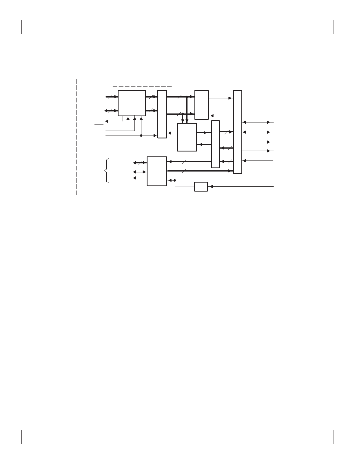
1.3 Functional Block Diagram
Microcontroller Interface
MCA
MCS
MRW
BCLK
Data
Port
7
Byte Stacker
16
DM D0–D15
DM Control
DMCLK
8-/16-to-32
bits
32
16
Figure 1–1. TSB12L V32 Functional Block Diagram
MA0 – MA6
MD0 – MD15
Mover
7
Data
Mover
DM
Address
7
Data
32
Host Interface
FIFO
2K ATF
2K GRF
32
32
CFR
ATF
GRF
DM IR/IR
DM IT/AT
÷ 2
Control
Status
ATF
32
Link Core
ARF
32
IRF
32
Packet Router Control
CTL[0:1]
D[0:7]
LREQ
LPS
LinkOn
Physical Layer Chip (PHY)
SCLK
1–2
Page 11
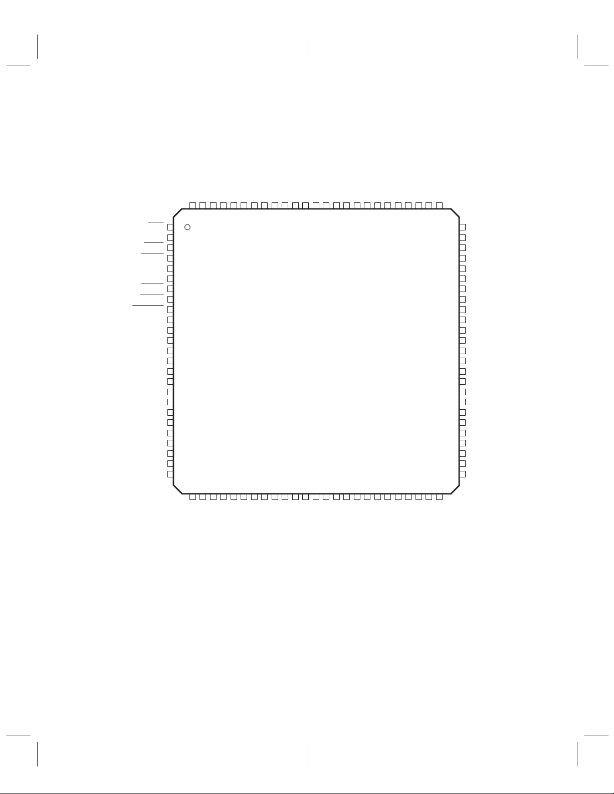
1.4 Terminal Assignments
PZ PACKAGE
(TOP VIEW)
INT
CYSTART
TEA
MCA
GND
BCLK
MCS
MWR
RESET
VDD5V
MDINV
COLDFIRE
M8BIT/SIZ0
MCMODE/SIZ1
V
DD
TESTMODE
MA6
MA5
MA4
V
DD
MA3
MA2
MA1
MA0
GND
1
2
3
4
5
6
7
8
9
10
11
12
13
14
15
16
17
18
19
20
21
22
23
24
25
MD0
GND
99
100
27
26
MD1
MD2
97
98
28
29
MD3
V
95
96
31
30
DD
MD4
MD5
93
94
33
32
MD6
MD7
91
92
TSB12LV32
35
34
MD8
GND
89
90
37
36
MD9
88
38
MD10
MD11
86
87
40
39
DD
MD12
V5V
84
85
42
41
MD14
MD13
82
83
44
43
DD
MD15
V
80
81
46
45
DIRECT
GND
DMREADY
77
78
79
49
48
47
CYCLEIN
76
LENDIAN
75
LREQ
74
GND
73
SCLK
72
71
V
70
CTL0
69
CTL1
68
V
67
D0
66
D1
65
CONTNDR
64
LINKON
63
D2
62
D3
61
D4
D5
60
59
D6
58
D7
GND
57
56
STAT2
55
STAT1
54
STAT0
53
LPS
52
DMERROR
51
PKTFLAG
50
DD
DD
DMD0
DMD1
DMD2
DMD3
GND
DMD4
DMD6
DMD5
DD
DMD7
V5V
DMD9
DMD8
DD
V
DMD11
DMD10
DMD12
DMD14
DMD13
GND
DMD15
DMCLK
DD
V
DMPRE
DMRW
DMDONE
1–3
Page 12
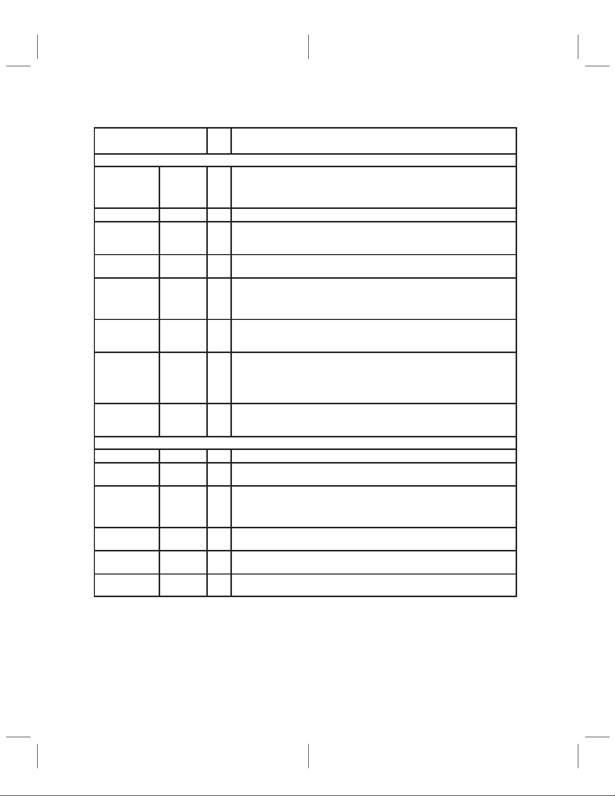
1.5 Terminal Functions
I/O
DESCRIPTION
The terminal functions are described in Table 1–1.
T able 1–1. Terminal Functions
TERMINAL
NAME NO.
Microcontroller/Microprocessor Interface
BCLK 6 I Microinterface clock. Maximum frequency is 60 MHz. In the ColdFire mode,
COLDFIRE 12 I ColdFire mode. To operate in this mode, COLDFIRE must be asserted high.
LENDIAN 75 I Little-endian mode for the microinterface. When this terminal is pulled up, the
MA0 – MA6 24 – 21
19 – 17
M8BIT/SIZ0 13 I Configuration bit for microinterface. If the microinterface is 8 bits wide, this
MCMODE/SIZ1 14 I Mode bit for microinterface. If the microinterface wants to communicate in a
MCA 4 O Microinterface cycle acknowledge. When asserted low, MCA signals an
MCS 7 I Microinterface cycle start. When asserted low, MCS signals the beginning of a
MDINV 11 I Microinterface data invariant mode. This terminal is meaningful only when
MD0 – MD15 99 – 96
94 – 91
89 – 86
84 – 81
MWR 8 I Microcontroller read/write indicator. When asserted high, MWR indicates a read
TEA 3 O Transfer error acknowledge. This active-low signal is asserted low for one BCLK
BCLK is the same as CLK, which is the clock-input signal to the ColdFire.
data on MD0–MD15 will be byte-swapped to little endian byte format before it is
written to the CFR or FIFO and after it is read from the CFR or FIFO.
I Microcontroller address bus. MA0 is the most significant bit (MSB) of these 7 bits.
terminal must be pulled up to the supply voltage. In ColdFire mode, this terminal
represents burst SIZ0.
handshake manner this terminal must be pulled up to the supply voltage. When
the ColdFire mode terminal (12) is high, this terminal represents burst SIZ1.
acknowledge of the microcontroller cycle from the TSB12L V32.
microcontroller operation to the TSB12L V32.
LENDIAN (75) is high. When asserted high, the microinterface operates in the
data invariant mode. When low, the microinterface operates in address invariant
mode.
I/O Microinterface bidirectional data bus. MD0 is the most significant bit. However,
byte significance is dependent on the state of the LENDIAN and MDINV
terminals.
access from the TSB12LV32. When asserted low , MWR
to the TSB12LV32.
cycle whenever there is an illegal transfer request by the microcontroller (i.e.,
requested data transfer size is unsupported or MCS
one BCLK cycle in ColdFire mode).
indicates a write access
is asserted low for more than
1–4
Page 13
T able 1–1. Terminal Functions (Continued)
I/O
DESCRIPTION
TERMINAL
NAME NO.
Data-Mover Port Interface
DMD0–DMD15 26 – 29
31 – 34
36 – 39
41 – 44
DMCLK 46 O Data mover clock at (SCLK/2) MHz
DMDONE 50 O Data mover done. For transmit, this will be activated when the packet per block
DMERROR 52 O Data mover error. DMERROR is asserted high when there is an error in the
DMPRE 48 O Data mover predata indicator. In transmit mode, DMPRE pulses for one DMCLK
DMREADY 77 I Data mover ready. Must be asserted high by the external logic controlling the DM
DMRW 49 O Data mover read/write indicator. When data is being moved from 1394 to the DM
PKTFLAG 51 O Packet flag. When set, PKTFLAG is asserted high to indicate the first (header) or
CTL0, CTL1 70, 69 I/O Phy-link interface control lines.
D0–D7 67, 66,
63–58
LINKON 64 I Link-on from the Phy is a 4 MHz – 8 MHz clock. This signal will be activated when
LPS 53 O Link power status. LPS is used to drive the LPS input to the Phy. It indicates to the
LREQ 74 O Link request to Phy. LREQ makes bus requests and register access requests to
SCLK 72 I System clock. SCLK is a 49.152 MHz clock supplied by the Phy. DMCLK is
I/O Data mover (DM) bidirectional data port. DMD0 is the MSB of these 16 bits.
counter in the CFR counts down to zero. For receive, this terminal will pulse for
one DMCLK prior to the first byte/word available to the DM interface.
received packet or an illegal transmit speed was attempted.
prior to sending the first quadlet. In isochronous receive mode, DMPRE will pulse
for one DMCLK when the sync bit in the header matches a bit set in the
isochronous register. DMPRE is not used in asynchronous receive mode.
interface when it is ready to supply data for transmit. DMREADY must be set low
when the data mover is in receive mode.
port (receive) this signal will go active high to indicate data is available on
DMD[0:15]. When data is being moved from DM to 1394 bus (transmit) this signal
will go active high to indicate that data must be supplied to the DMD[0:15] port for
transmission.
last (trailer) quadlet of a received packet on the DM interface. PKTFLAG is not
valid in transmit mode.
Phy/Link Interface
I/O Phy-link interface data lines. Data is only expected on D0 and D1 at 100 Mbit/s,
D0–D3 at 200 Mbit/s, and D0–D7 at 400 Mbit/s. D0 is the MSB bit.
the link is inactive and the Phy has detected a link-on packet or a Phy interrupt.
This clock will persist for no more than 500 ns. When the link detects this terminal
as active, it will turn on and drive LPS.
Phy that the link is powered up and active. LPS toggles at a rate = 1/16 of BCLK.
the Phy.
generated from SCLK.
1–5
Page 14
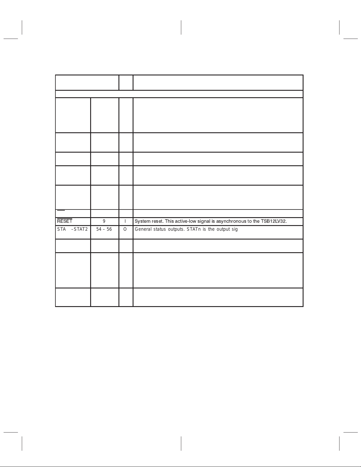
T able 1–1. Terminal Functions (Continued)
I/O
DESCRIPTION
TERMINAL
NAME NO.
Miscellaneous Functions
CONTNDR 65 I/O Contender. When asserted high, this terminal tells the link that this node is a
CYCLEIN 76 I Cycle in. This input is an optional external 8-kHz clock used as the isochronous
CYSTART 2 O Isochronous cycle start indicator. CYSTAR T signals the beginning an isochronous
DIRECT 79 I Isolation terminal. When this terminal is asserted high, no isolation is present
GND 5, 25, 30,
INT 1 O Interrupt. NOR of all internal interrupts.
RESET
STAT0–STAT2 54 – 56 O General status outputs. STATn is the output signal selected with the CFR at
TESTMODE 16 I This terminal is used to place the TSB12LV32 in the test mode. In normal
VDD5V 10, 35, 85 5 V (± 0.5V) supply voltage for 5-V tolerant inputs. Only the Phy/link interface side
V
DD
45, 57, 73,
78, 90,
100
9 I
15, 20, 40,
47, 68, 71,
80, 95
contender for isochronous resource manager (IRM) or bus manager functions.
The state of the CONTNDR must match the state of the Phy contender terminal for
1394-1995 compliant Phys, and the Phy register bit for 1394.A compliant Phys.
This terminal defaults to being an input on power up. After power up, the value of
this terminal may be driven internally by the CTNDRSTAT bit (bit#12 at 08h)
cycle clock. It should only be used if attached to the cycle-master node. It is
enabled by the cycle source bit and should be tied high when not used.
cycle by pulsing for one DMCLK period.
between the TSB12LV32 and the Phy. When low, bus holder isolation becomes
active.
Ground reference
System reset. This activeĆlow signal is asynchronous to the TSB12LV32.
address 20h.
operation, this terminal must be tied to ground.
of the TSB12LV32 is not 5-V tolerant. T ie this terminal to the 3.3-V supply voltage if
the TSB12LV32 is not connected to any devices driving 5-V signals. Tie this
terminal to the 5-V supply voltage if the TSB12L V32 is connected to any devices
driving 5-V signals. This terminal is only used to make inputs 5-V tolerant, it is not
used for any outputs.
3.3 V (± 0.3 V) supply voltage
1–6
Page 15
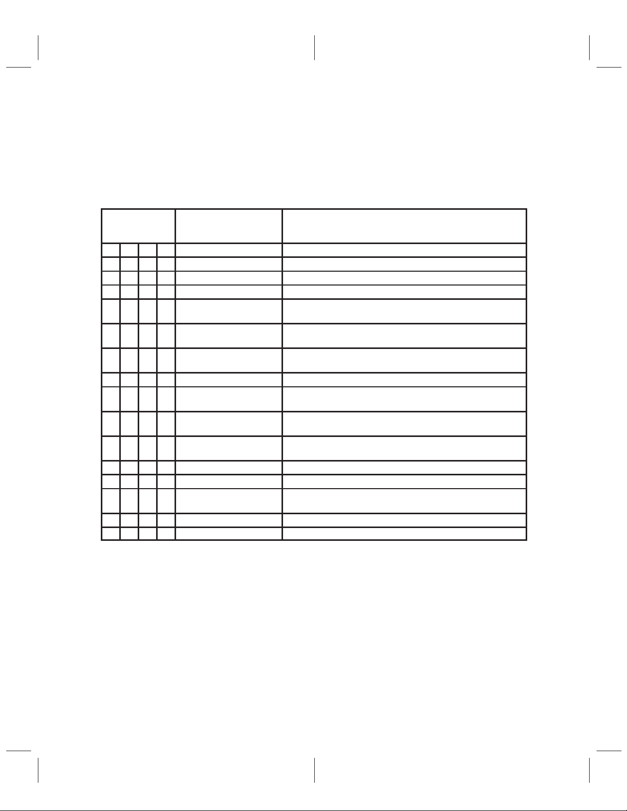
1.5.1 STAT0, STAT1, and STAT2 Programming
ST AT0, ST AT1 and ST AT2 terminals can be independently programmed to show one of fourteen possible
internal hardware status. The controls for the ST AT terminals are in the
of the CFR register. STAT0 is controlled by STATSEL0(bits 16–19), STAT1 is controlled by bits
STATSEL1(bits 20–23), and STAT2 is controlled by STATSEL2 (bits 24–27). Refer to Table 1–2 for
programming the STAT terminals.
T able 1–2. STAT Terminals Programming
STATSEL0,
STATSEL1, or
STATSEL2
0 0 0 0 Reserved Reserved
0 0 0 1 ATFFULL ATF is full. Bit 12 in CFR at 30h.
0 0 1 0 Bus Reset 1394 Bus reset. Bit 3 in CFR at 0Ch
0 0 1 1 Arbitration reset gap Bit 26 in CFR at 0Ch
0 1 0 0 CYCLEOUT
0 1 0 1 RXDMPKT
0 1 1 0 RXGRFPKT
0 1 1 1 BX_BUSY Byte busy. This represents the OR of bits 0 – 3 of CFR at 20h
1 0 0 0 SUBGP
1 0 0 1 CYCLE_DONE
1 0 1 0
1 0 1 1 DMACKERR DM acknowledge was not Complete. Bit 17 in CFR at 0Ch
1 1 0 0 DMEN DM enable. Bit 26 in CFR at 04h
1 1 0 1
1 1 1 0 Reserved Reserved
1 1 1 1 Reserved Reserved
STAT0/STAT1/STAT2 DESCRIPTION
Cycle out. This is the link’s cycle clock. It is based on the timer
controls and the received cycle-start messages.
Packet received to DM interrupt. Activated at the end of a received
packet. Bit 9 in CFR at 0Ch
Packet received to GRF interrupt. Activated at the end of a received
packet. . Bit 6 of CFR at 0Ch
Subaction gap. Activated upon detection of a subaction gap. Bit 27
in CFR at 0Ch
Cycle done. Indicates the end of the isochronous period. This
happens when a subaction gap has been detected.
ATSTARTED
(default setting for STAT1)
GRFEMPTY
(default setting for STAT2)
Activated when an asynchronous packet transfer has started from
the ATF. Bit 5 in CFR at 0Ch
GRF is empty. Bit 15 in CFR at 30h.
Diagnostic
register at address 20h
1–7
Page 16

1–8
Page 17

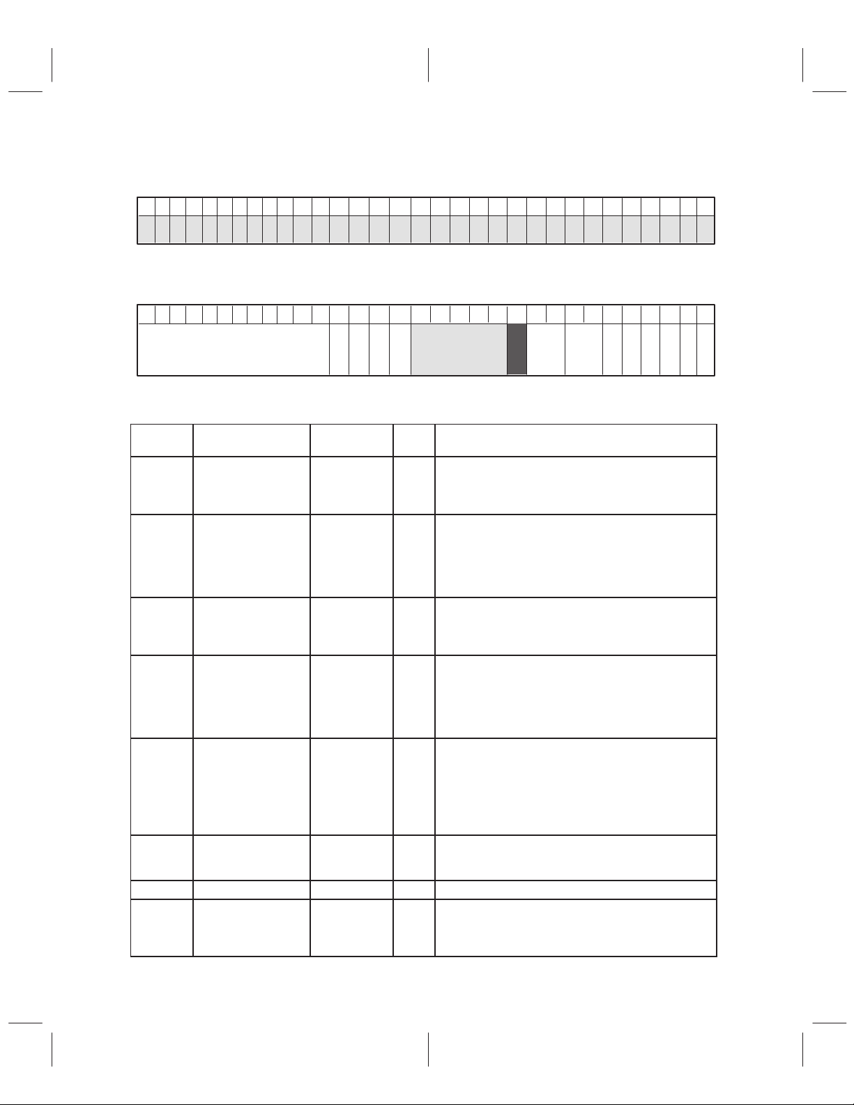
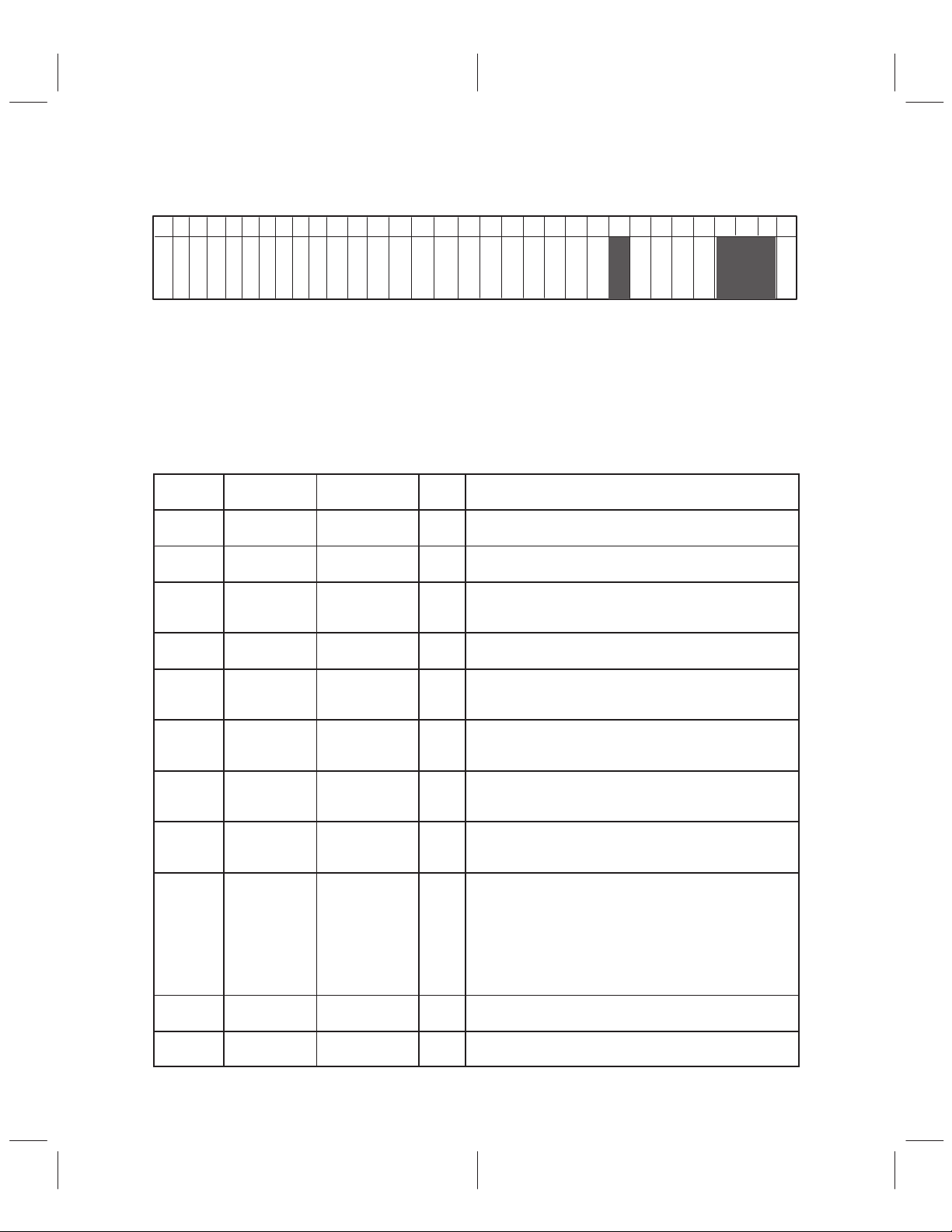
2 Internal Registers
2.1 TSB12LV32 Configuration Registers
2–1
Page 18
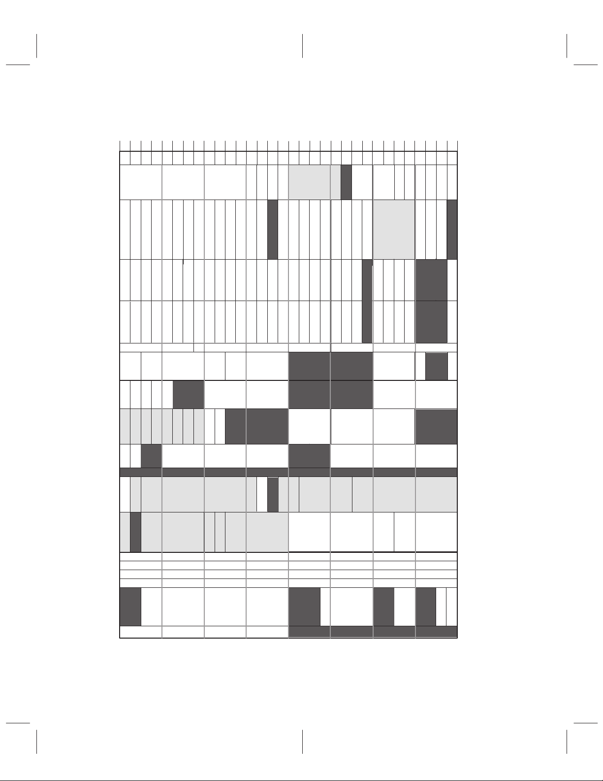
Table 2–1. Configuration Register (CFR) Map
MSB LSB
0123456789101112131415161718192021222324252627 293031
01110001000101010011100010100000
00h
AUTOUP
HANDSHK
BDIV0
BUSNRST
SNTRJ
TCERR
HDRERR
SNTRJ
TCERR
HDRERR
DMACK
BDIV1
DMACKCOMP
FIFOACK
DMACKERR
FIFOACK
DMACKERR
CYTEN
CYSRC
CYMAS
FIFOACKCOMP
CYST
CYSEC
CYST
CYSEC
CYDNE
CYDNE
MCERROR
MCERROR
SPEED
CHNLCNT
SID
ERROR
CODE
CLSIDER
CYLST
CARBFL
CYLST
CARBFL
CYCLE OFFSET
ISYNCRCVN
DMEN
DMHDR
SUBGP
ARBGP
SUBGP
ARBGP
PING VALUE
04h
PACKET PER BLOCK
08h
TXEN
RXSLD
FULLSID
0Ch
10h
14h
18h
1Ch
FLSHERR
INT
INT
E_HCRC
PHY_PKT_ENA
PHINT
PHRST
PHRRX
PHINT
PHRST
PHRRX
SECONDS COUNT CYCLE COUNT
IRPORT1
TAG1
F_ACK
NO_PKT
E_DCRC
RXEN
BSYCTL
RXGRFPKT
SELFIDEND
ATSTARTED
RXGRFPKT
SELFIDEND
ATSTARTED
NO_ACK
ENA_ACCEL
ENA_CONCAT
ENA_INSERT_IDLE
CMDRST
DMERROR
RXDMPKT
CMDRST
DMERROR
RXDMPKT
TAG2
ENDSWAP
RSTTX
RSTRX
CTNDRSTAT
LINKONLINKON
ATSTK
SELFIDER
ATSTK
SELFIDER
IRPORT2
ACK
BYTEMODE
CTNDRISIN
ATFEMPTY
ATFEMPTY
28
AR0
CMAUTO
IRCVALL
AR1
DMASYNC
IRP1EN
IRP2EN
VERSION
(711538A0h)
DM Control
DMRX
Control
Interrupt
IARBFL
Interrupt
Mask
IARBFL
Cycle Timer
Isochronous
Port
MONTAG
Maint_Control
20h
B3_PND
RAM_TEST
REGRW
24h
B0_BUSY
B1_BUSY
RDPHY
WRPHY
B1_PND
B2_PND
B0_PND
B2_BUSY
B3_BUSY
PHYRGAD PHYRGDATA
28h–2Ch
30h
34h
ATFCLR
ATFWBMTY
NRIDVAL
NODECNT
ATFAVAIL
GRFCLR
ATFFULL
IRMNODEID BUS NUMBER NODE NUMBER
ROOT
CONTENDER
38h
3Ch
40h
44h
48h
ASYNC RETRY COUNT RETRY INTERVAL
4Ch
NUMBER OF QUADLETS
NOTES: A. All dark gray areas (bits) are reserved bits.
B. All light gray areas are read-only bits. All remaining are read/write bits.
2–2
STATSEL0 STATSEL1 STATSEL2
PHYRXAD PHYRXDATA
CD
ATACK GRFUSED
GRFEMPTY
ACKCODE SPD
Diagnostic
Phy Access
Reserved
FIFO Status
Bus Reset
Header0
Header1
Header2
Header3
Trailer
LPS_OFF
LPS_RESET
Asynchronous
Retry
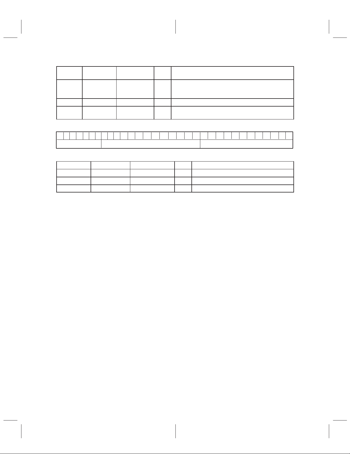
Page 19

DIRECTION
y
Asynchronous
OF DM DATA
TRANSFER
TRANSMIT
(to 1394 Bus)
RECEIVE
(from 1394
Bus)
PACKET TYPE
Isochronous
Asynchronous/
asynchronous
streaming
Isochronous/
asynchronous
streaming
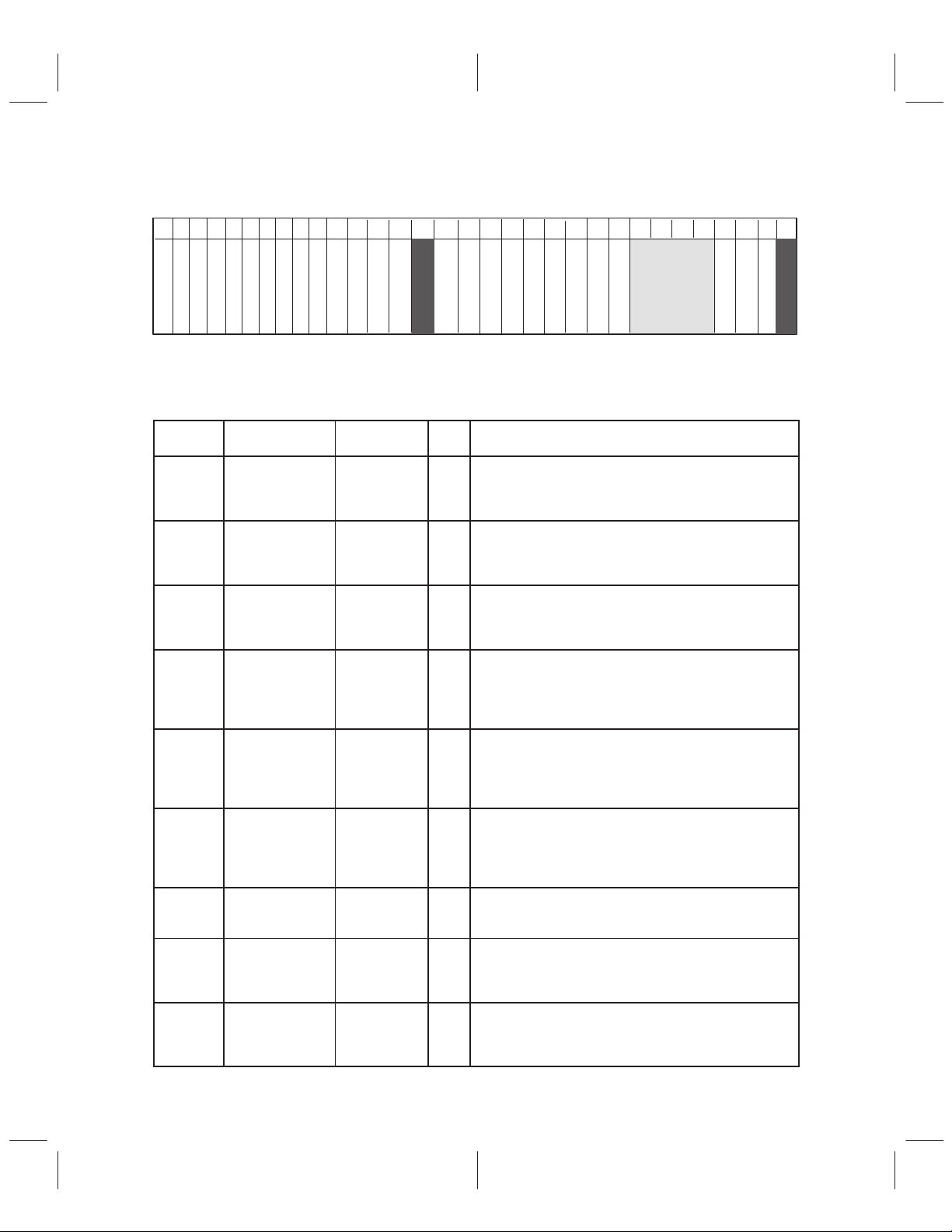
T able 2–2. Header Usage for CFRs 38h–44h
AUTO HEADER
INSERT/
EXTRACT
YES
NO
YES
NO
YES
NO
YES
NO
Header 0 CFR formatted for isochronous transmission.
Header1 – Header3 are used for additional channels.
Isochronous header supplied by DM interface. Header0 CFR
is automatically written with extracted (from transmitted
packet) isochronous header.
Header0–Header3 CFRs formatted for asynchronous transmission.
Asynchronous header supplied by DM interface. Header0 –
Header3 CFRs are automatically written with extracted (from
transmitted packet) header.
Header0 – Header3 are always automatically updated. The
isochronous header is streamed through the DM port. The
trailer quadlet is always appended to the data stream.
Header0 – Header3 are always automatically updated. The
isochronous header is streamed through the DM port along
with the payload data. The trailer quadlet is always appended
to the data stream.
Header0 – Header3 are always automatically updated.
Asynchronous headers are not streamed through the DM
port. The trailer quadlet is always appended to the data
stream.
Header0 – Header3 are always automatically updated.
Asynchronous headers are streamed through the DM port
along with data. The trailer quadlet is always appended to the
data stream.
HEADER REGISTER
2–3
Page 20
2.2 Configuration Register Definitions
2.2.1 Version Register at 00h
0 1 2 3 4 5 6 7 8 9 10 11 12 13 14 15 16 17 18 19 20 21 22 23 24 25 26 27 29 30 3128
01110001000101 0 10 011100010100000
This register uniquely identifies this device to the software. The value is fixed at 7115_38A0’h. This register
is read only .
2.2.2 Data Mover Control Register at 04h
0 1 2 3 4 5 6 7 8 9 10 11 12 13 14 15 16 17 18 19 20 21 22 23 24 25 26 27 29 30 3128
PACKET PER BLOCK
ENDSWAP
AUTOUP
HANDSHK
BYTEMODE
DMACK
SPEED
DMEN
CHNLCNT
AR0
DMHDR
AR1
DMASYNC
This register controls the Data Mover port and must be set up before using the port. The power-up reset
value of this register = 0000_0000’h
BIT
NUMBER
0–11 PACKET PER-
12 ENDSWAP Endian Swap R/W Swap endian. When this bit is set, the quadlet formed by
13 BYTEMODE Byte Mode R/W Byte mode. When this bit is set the DM port will only look
14 HANDSHK Handshake
15 AUTOUP Automatic
16–20 DMACK DM
21 RESERVED RESERVED
22–23 SPEED DM Speed
BIT NAME FUNCTION DIR DESCRIPTION
BLOCK
Packets per
Block
R/W Number of packets per block. A packet is the size of the
data payload and is specified as part of the header. The
data mover logic uses this value to deactivate DMDONE.
This field is only used in transmit mode.
stacking the DM data will be byte reversed, (i.e. the
quadlet formed by fetching doublet AB01 then ‘CD02’ will
be 02CD–01AB instead of AB01CD02). In byte mode the
quadlet formed by fetching AB, 01, CD, 0 will be
02CD01AB instead of AB01CD02.
at DM0–DM7. DM8–DM15 will be ignored for transmit
and will not be driven on receive. In this mode, the
maximum speed allowed is 200 Mbps.
R/W Handshake. When this bit is 1 DMREADY and DMDONE
Mode
(CPLynx
Mode)
are in strict handshake mode (i.e., TSB12LV31
compatible mode). DMREADY must not be deactivated
until DMDONE activates. When this bit is set to 0,
DMREADY may be deactivated before DMDONE
activates.
R/W Automatic update offset address. Valid only for
Address Up-
date
asynchronous transmit using header insert mode (bit 27
DMHDR set to 1). For write request asynchronous
packets, header quadlet 2 contains the destination offset
low address for the write. When this bit is set, header
quadlet 2 will be updated by the value of the payload size
(rounded up to the nearest quadlet boundary).
R DM acknowledge. This is the ack received from the
Acknowledge
receiving node. This is updated only when the transfer is
from the DM port.
R/W Speed code. This is valid for isochronous transmit and
Code
asynchronous transmit through the DM port. The DM
logic uses this field to specify to the Phy the speed of the
isochronous transfer.
DMRX
2–4
Page 21

BIT
NUMBER
24–25 CHNLCNT Channel
Count
26 DMEN DM Enable R/W DMEN controls the transmission of packets from the DM
27 DMHDR DM Header
Insert Control
28–29 AR0, AR1 Receive
Control
Routing
30 DMASYNC DM
Asynchronous
31 DMRX DM Receive R/W If this bit is set to 1 the DM port is configured to receive.
R/W Channel count. This field is valid only in isochronous
transmit. This field allows the node to transmit multiple
packets during a single isochronous period. Each packet
must have a different channel number, however,
hardware does not check this. When the isochronous
transmit header is supplied by the DM interface or
automatically inserted by the hardware, a maximum of
four different channels may be accessed in one
isochronous period. In isochronous transmit with
automatic header insert, Header0–Header3 CFRs are
used as the isochronous header registers.
port. If this bit is 0, transmission through from the DM port
is inhibited. This is used for asynchronous flow control. In
normal operation, if an asynchronous packet transmitted from the DM port receives an acknowledge from
the receiving node other than
be set to 0 and DMERROR is asserted high. Software will
need to set this bit to allow further transmission of
asynchronous packets from the DM port. The default and
power-up value is 0.
R/W DM header insert bit. When set to 0, the hardware will
automatically insert the header(s) into the DM transmit
data. In receive, setting this bit to 0 will strip off the
header(s) before routing packet to the DM. Header(s) are
always written to the CFR header registers regardless of
the value of DMHDR.
R/W Receive packet routing control encoded bits. These bits
in conjunction with DMASYNC and DMRX bits in the DM
control register controls the routing of the received
packet to either the data mover port or to the GRF . Refer
to Table 4–1.
R/W If this bit is set to 1 the DM port is configured for
asynchronous traffic only. The DM port can not accept
both asynchronous and isochronous traffic. It must be
configured for asynchronous (DMASYNC = 1) or
isochronous (DMASYNC = 0).
The DM port cannot both transmit and receive data at the
same time, it must be configured for either transmit or
receive.
DESCRIPTIONDIRFUNCTIONBIT NAME
ack complete
, this bit will
2–5
Page 22
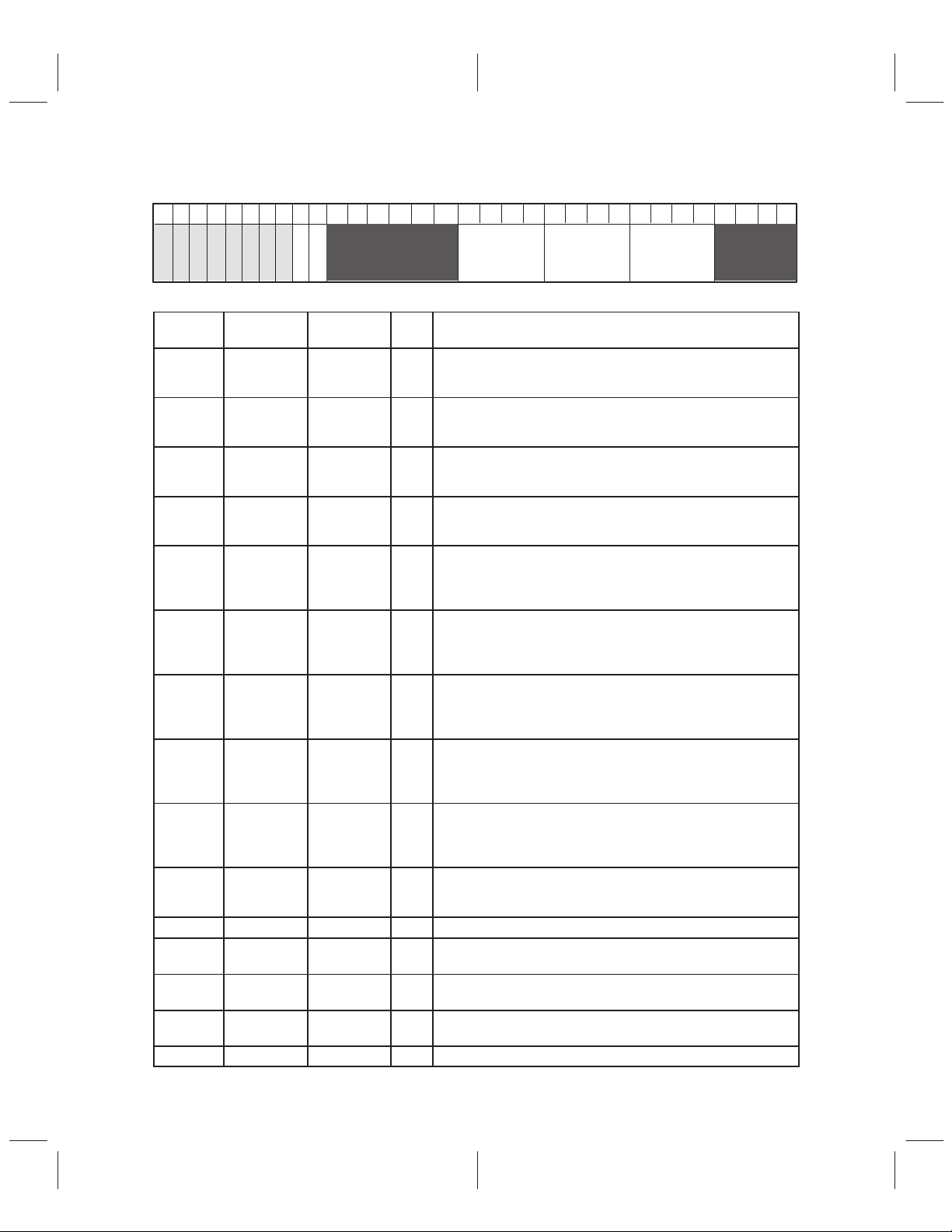
2.2.3 Control Register at 08h
0 1 2 3 4 5 6 7 8 9 10 11 12 13 14 15 16 17 18 19 20 21 22 23 24 25 26 27 29 30 3128
RXSID
FLSHERR
FULLSID
BSYCTRL
PHY_PKT_ENA
TXEN
RXEN
ENA_ACCEL
RSTTX
ENA_CONCAT
ENA_INSERT_IDLE
RSTRX
CTNDRSTAT
CTNDRISIN
BDIV0
BUSNRST
BDIV1
DMACKCOMP
CYSRC
CYMAS
FIFOACKCOMP
CYTEN
SIDERCODE
CLSIDER
IRP1EN
CMAUTO
IRP2EN
The control register dictates the basic operation of the TSB12L V32. The power-up reset value of this register
equals E004_0200’h
BIT
NUMBER
0 FLSHERR Flush GRF
1 RXSID Received
2 FULLSID Save full
3 PHY_PKT_ENA Phy Packets
4 BSYCTRL Busy Control R/W BSYCTRL controls which busy status the chip returns to
5 TXEN Transmit
6 RXEN Receive
7 ENA_ACCEL Acceleration
8 ENA_CONCAT Concatenation
BIT NAME FUNCTION DIR DESCRIPTION
R/W This bit controls the flushing of the GRF when a packet with
on error
a data CRC error is detected. The power–up value is 1,
which means flush the GRF when a data CRC error is
detected.
R/W If set, the self-identification (SID) packets generated by Phy
Self-ID
packets
devices during the bus initialization are received and placed
into the GRF as a single packet. The default setting of this
bit is 1. When set to 0, the SIDs are not placed into the GRF .
R/W Save the full self-ID packets.When this bit is 1 the self-ID
Self-ID Packet
in GRF
data quadlet and its inverse quadlet are saved in the GRF.
When this bit is 0 only the self-ID data quadlet is saved in the
GRF .
R/W Phy packet enable allows reception of all Phy packets. If this
Receive
Enable
bit is reset to 0, all Phy packets, except for self-IDs, will be
rejected and interrupt HDERR (if not masked) will be
generated. One HDERR interrupt will be generated for
every Phy packet received.
incoming packets. When this bit is 0 the chip follows normal
busy/retry protocol, only send busy when necessary. When
this bit is 1 the chip sends a busy acknowledge to all
incoming packets following the normal busy/retry protocol.
R/W When TXEN is cleared, the transmitter does not arbitrate or
Enable
send packets. TXEN bit is cleared following a bus reset, and
all traffic through the DM port will be interrupted. TXEN must
be set before packet transmit can resume. Power-on reset
value of TXEN is 0
R/W When RXEN is cleared, the receiver does not receive any
Enable
packets. This bit is not affected by a bus reset and is set to 0
after a power-on reset.
R/W Enable acceleration. When this bit is set, fly-by acceleration
Enable
and accelerated arbitration are enabled. This bit cannot be
set while TXEN and RXEN are set. This bit must only be
used with a 1394a capable Phy.
R/W Enable concatenation. When this bit is set it allows the link
Enable
to concatenate multiple isochronous or asynchronous
packets. This bit must only be used with a 1394a capable
Phy.
2–6
Page 23
BIT
NUMBER
9 ENA_
INSERT_IDLE
Insert Idle
Enable
DESCRIPTIONDIRFUNCTIONBIT NAME
R/W Per P1394a, the link is required to insert an idle state on the
control lines after the Phy grants the link control of the
Phy/link interface. If using a P1394a Phy, this bit should be
set to 1 in order for the link to drive an idle state following the
grant state from the Phy. For 1394-1995 Phys this bit must
remain low.
10 RSTTX Transmitter
Reset
11 RSTRX Receiver
Reset
12 CTNDRSTAT Contenter
status
13 CTNDRISIN Contender
Driver Enable
14 RESERVED Reserved
15 BUSNRST Bus number
reset enable
16–17 BDIV0, BDIV1 BCLK divisor
encode bits
R/W When RSTTX is set, the entire transmitter resets
synchronously. This bit clears itself.
R/W When RSTRX is set, the entire receiver resets
synchronously. This bit clears itself.
R/W Contender status. On power up, this bit reflects the status of
the CONTNDR pin. When bit 13, CTNDRISIN, is 0 this bit
will be driven out to the CONTNDR pin. If CTNDRISIN is 1
this bit is not used. (Only use on 1394–1995 Phys, or
P1394a Phys when using hardware reset, otherwise, use
the 1394a Phy registers to set the nodes contender status).
R/W Driver enable for the CONTNDR pin. On power up this bit is
set to 1 which disables the driver and allows reading of the
state of the CONTNDR pin. Writing a 0 to this bit will enable
the driver and will drive bit 12, CTNDRSTAT, to the
CONTNDR pin.
R/W When this enable is set to high, the bus number field clears
to 3FFh when a local bus reset is received.
R/W
BCLK divisors encode bits. Used to divide down the BCLK
to generate the link power status (LPS) clock to the Phy.
BDIV0 BDIV1 DESCRIPTION
0 0 Divide by 16. Default power on value.
0 1 Divide by 2. Recommended for BCLK
1 0 Divide by 4. Recommended for BCLK
1 1 Divide by 32. Recommended for BCLK
Recommended for BCLK frequencies in
the range of 8 – 88 MHz.
frequencies in the range of 1 – 1 1 MHz.
frequencies in the range of 2 – 22 MHz.
frequencies in the range of 16 – 176
MHz
18 DMACKCOMP Data Mover
Acknowledge
Complete
19 FIFOACKCOMP FIFO
Acknowledge
Complete
R/W Data mover acknowledge complete. This bit controls the
acknowledge response to an asynchronous packet
received and routed to the DM port. The default and power
on value is 0 which means to respond with ack pending. A 1
means to respond with an ack complete for write request
packets.
R/W FIFO acknowledge complete. This bit controls the
acknowledge response to an asynchronous packet
received and routed to the GRF. The default and power on
value is 0 which means to respond with ack pending. A 1
means to respond with ack complete.
2–7
Page 24
BIT
NUMBER
20 CYMAS Cycle Master R/W When CYMAS is set and the TSB12LV32 is attached to the
21 CYSRC Cycle Source R/W When CYSRC is set, the cycle_count field increments and
22 CYTEN Cycle timer
enable
23 CLRSIDER Self-ID
error-code
clear
24–27 SIDERCODE Self-ID error
code
28 CMAUTO Auto set cycle
master
29 IRP1EN IR port 1
enable
30 IRP2EN IR port 2
enable
31 RESERVED Reserved
root Phy, the cyclemaster function is enabled. When the
cycle_count field of the cycle timer register increments, the
transmitter sends a cycle-start packet.
the cycle_offset field resets for each positive transition of
CYCLEIN. When CYSRC is cleared, the cycle_count field
increments when the cycle_offset field rolls over .
R/W When CYTEN is set, the cycle_offset field increments.
W When CLRSIDER is set, the SIDERCODE field (bits 24–27)
is cleared.This bit clears itself.
R
SIDERCODE contains the error code of the first Self-ID
Error. The error code is as follows:
0000 No error
0001 Last self-ID received was not all child ports
0010 Received Phy ID in self-ID not as expected
0011 Quadlet not inverted (phase error)
0100 Phy ID sequence error (two or more gaps in IDs)
0101 Phy ID sequence error (large gap in IDs)
0110 Phy ID error within packet
0111 Quadlet not the inversion of the prior quadlet
1000 Reserved
R/W When CMAUTO is high, the TSB12LV32 automatically
enables CYMAS when the this node becomes the root
following a bus reset.
R/W When IRP1EN is set, the receiver accepts isochronous
packets when the channel number matches the value in the
IR port1 field at18h
R/W When IRP2EN is set, the receiver accepts isochronous
packets when the channel number matches the value in the
IR Port2 field at18h
DESCRIPTIONDIRFUNCTIONBIT NAME
2–8
Page 25
2.2.4 Interrupt/Interrupt Mask Register at 0Ch and 10h
0 1 2 3 4 5 6 7 8 9 10 11 12 13 14 15 16 17 18 19 20 21 22 23 24 25 26 27 29 30 3128
INT
PHINT
PHRST
PHRRX
RXGRFPKT
SELFIDEND
ATSTARTED
CMDRST
DMERROR
RXDMPKT
SELFIDER
ATSTK
LINKON
SNTRJ
ATFEMPTY
TCERR
HDRERR
FIFOACK
DMACKERR
CYSEC
MCERROR
CYST
CYDNE
CYLST
ARBGP
CARBFL
SUBGP
The interrupt and interrupt mask register work in tandem to inform the host bus interface when the state of
the TSB12L V32 changes. The interrupt register is at 0Ch, the interrupt mask register is at 10h. The interrupt
register powers up all 0s, however, the interrupt mask register powers up with the INT and the MCERROR
bit set, i.e. 8000_1000h. The mask bits allows individual control for each interrupt. A 1 in the mask bit field
allows the corresponding interrupt in the interrupt register to be generated. Once an interrupt is generated
it must be cleared by writing a 1 to the bit in the interrupt register. For testing, each interrupt bit can be set
manually . This is done by first setting the REGRW bit at20h and then setting the individual interrupt bit. This
is also true for bit 0 at0Ch. In this test mode, the interrupt mask register is not used and has no effect.
BIT
NUMBER
0 INT Interrupt R/W INT contains the value of all interrupt and interrupt mask bits
1 PHINT Phy chip
2 PHRRX Phy register
3 PHRST Phy reset
4 SELFIDEND Self-ID
5 ATSTARTED Asynchronous
6 RXGRFPKT GRF packet
7 CMDRST CSR register
8 DMERROR Data Mover
9 RXDMPKT Data Mover
10 SELFIDER Self-ID packet
BIT NAME FUNCTION DIR DESCRIPTION
ORed together
R/W When PHINT is set, the Phy has signalled an interrupt
interrupt
through the Phy interface
R/W When PHRRX is set, a register value has been transferred to
information
the Phy access register (offset 24h) from the Phy interface
received
R/W When PHRST is set, a Phy-LLC reconfiguration has started
started
(1394 bus reset)
R/W Self-ID end. This bit is set at the end of the self-ID reporting
validated
process. When this bit is set, the contentF of the bus reset
CFR at34h is valid.
R/W Asynchronous transfer started. Activated when the bus has
transfer started
been granted and the first quadlet from the FIFO is about to
be popped from the ATF.
R/W Receive packet to GRF . This bit is set whenever a complete
received
packet has been confirmed into the GRF (asynchronous or
isochronous).
R/W If CMDRST is set, the receiver has been sent a quadlet write
reset request
request to the Reset_Start CSR register(target address is
FFFF_F000_000Ch)
R/W DM error. This bit will be set whenever there is an error in the
error
DM stream. For transmit, if the DM port is configured for byte
access and the speed code in the DM control register or the
asynchronous header register is set for 400 Mbps then this
bit will be set. Under this condition DMEN will be reset to 0
preventing further transmit. For receive this bit will be set if
there is a header or data CRC error or if the DM port is configured for byte access and the data is received at 400 Mbps.
R/W Receive packet to DM. This bit is set whenever a packet is
packet receive
received to the DM port.
R/W Set if an error in the self-ID quadlet/packet has been de-
error
tected.
IARBFL
2–9
Page 26

BIT
NUMBER
11 LINKON Link-ON detect R/W Set if a link-on pulse is detected on the LINKON input termi-
12 ATSTK Transmitter is
stuck (AT)
13 ATFEMPTY ATF empty
interrupt
14 SNTRJ Busy
acknowledge
sent by receiver
15 HDRERR Header error R/W When HDRERR is set, the receiver detected a header CRC
16 TCERR Transaction
code error
17 DMACKERR Data Mover
acknowledge
error
18 FIFOACK FIFO
acknowledge
interrupt
19 MCERROR Micro-interface
error
20 CYSEC Cycle second
incremented
21 CYST Cycle started R/W When CYST is set, the transmitter has sent or the receiver
22 CYDNE Cycle done R/W When CYDNE is set, an arbitration gap has been detected
23 RESERVED RESERVED
24 CYLST Cycle lost R/W When CYLST is set, the cycle timer has rolled over twice
25 CARBFL Cycle
arbitration failed
26 ARBGP Arbitration gap R/W When ARBGP is set, the serial bus has been idle for an ar-
nal. This bit should be used by software to reactivate the LPS
output to the Phy .
R/W When ATSTK is set, the transmitter has detected invalid data
at the asynchronous transmit-FIFO interface. If the first
quadlet of a packet is not written to the ATF_First or
ATF_First&Update, the underflow of the ATF also causes an
ATStuck interrupt. When this state is entered, no asynchronous packets can be sent until the ATF is cleared by way of
the CLR ATF control bit. Isochronous packets can be sent
while in this state.
R/W ATFEMPTY. This bit is set to 1 when the ATF is empty.
R/W When SNTRJ is set, the receiver is forced to send a busy ac-
knowledge to a packet addressed to this node because the
GRF overflowed.
error on an incoming packet that may have been addressed
to this node.
R/W When TCERR is set, the transmitter detected an invalid
transaction code in the data at the transmit-FIFO interface.
R/W DM acknowledge error. Set to 1 when the acknowledge re-
ceived is not
of the DM Control CFR at04h will be reset to 0 and no more
asynchronous transmit from the DM port will be allowed to
take place until DMEN is set to 1.
R/W FIFO ack interrupt. This bit will be set when an acknowledge
from a previous ATF transmit has been received.
R/W Micro-interface error. Set whenever the microcontroller write
protocol is violated.
R/W When CYSEC is set, the cycle-second field in the cycle timer
register has incremented. This occurs about every second
when the cycle timer is enabled.
has received a cycle-start packet.
on the bus after the transmission or reception of a cycle-start
packet. This indicates that the isochronous cycle is over.
without the reception of a cycle-start packet. This occurs
only when this node is not the cycle master. All isochronous
traffic stop once CYLST is set. However , asynchronous and
asynchronous streaming traffic will not be affected.
R/W When CARBFL is set, the arbitration to send a cycle-start
packet has failed.
bitration reset gap.
ack complete
DESCRIPTIONDIRFUNCTIONBIT NAME
. When this occurs, DMEN(bit 26)
2–10
Page 27
BIT
NUMBER
27 SUBGP Subaction gap R/W When SUBGP is set, the serial bus has been idle for a subac-
28–30 RESERVED RESERVED
31 IARBFL Isochronous
arbitration failed
tion gap time (fair-gap). This bit can be set only when the
REGRW bit has been set in the diagnostics register at 20h.
R/W When IARFL is set, the arbitration to send an isochronous
packet has failed.
DESCRIPTIONDIRFUNCTIONBIT NAME
2.2.5 Cycle Timer Register at 14h
0 1 2 3 4 5 6 7 8 9 10 11 12 13 14 15 16 17 18 19 20 21 22 23 24 25 26 27 29 30 3128
SECOND COUNT CYCLE OFFSETCYCLE COUNT
This register must be written to as a quadlet. The power-up reset value of this register = 0000_0000’h
BIT NUMBER BIT NAME FUNCTION NAME DIR DESCRIPTION
0–6 Seconds_count Seconds count R/W 1-Hz cycle timer counter
7–19 Cycle_count Cycle count R/W 8,000-Hz cycle timer counter
20–31 Cycle_offset Cycle offset R/W 24.576-MHz cycle timer counter
2–11
Page 28

2.2.6 Isochronous Port Register at 18h
0 1 2 3 4 5 6 7 8 9 10 11 12 13 14 15 16 17 18 19 20 21 22 23 24 25 26 27 29 30 3128
TAG1
IRPORT1 IRPORT2 ISYNCRCVN
TAG2
The power-up reset value of this register = 0000_0000h
BIT
NUMBER
0–1 TAG1 Tag Field 1 R/W The TAG1 field can further qualify the isochronous reception
2–7 IRPORT1 Isochronous
8–9 TAG2 Tag Field 2 R/W The TAG2 field can further qualify the isochronous reception
10–15 IRPORT2 Isochronous
16–23 RESERVED Reserved
24–27 ISYNCRCVN Synchronous
28 IRCVALL Receive all
29–30 RESERVED Reserved
31 MONTAG Match on tag R/W MONTAG is set when the user wants to only accept
BIT NAME FUNCTION DIR DESCRIPTION
for isochronous Receive PORT1 when the MONT AG bit is set.
R/W IR port1 contains the channel number of the isochronous
receive port
1 channel
number
packets that the receiver accepts. The receiver accepts
isochronous packets with this channel number when the
IRP1EN is set.
for isochronous Receive PORT2 when the MONT AG bit is set.
R/W IR port2 contains the channel number of the isochronous
receive port
2 channel
number
packets that the receiver accepts. The receiver accepts
isochronous packets with this channel number when the
IRP2EN is set.
R/W In isochronous receive mode to the DM port, when the
Enable
ISYNCRCVN enable bits are high, the DMPRE terminal pulses
when an isochronous packet is received whose SYNC bit field
in its header matches the bit pattern in this field. The default is
0000b.
R/W When the IRCVALL bit is set high, the TSB12L V32 receives all
isochronous
packets
isochronous packets regardless of the channel number or tag
number. The default is off.
isochronous packets that match both the tag field and the
channel number field. When set, MONTAG indicates that
isochronous receive data is accepted. The default is off.
IRCVALL
MONTAG
2–12
Page 29
2.2.7 Maint_Control Register at 1Ch
0 1 2 3 4 5 6 7 8 9 10 11 12 13 14 15 16 17 18 19 20 21 22 23 24 25 26 27 29 30 3128
PING VALUEACK
E_HCRC
E_DCRC
F_ACK
NO_PKT
NO_ACK
This register is used to generate test conditions. The control bits in this register allow errors to be inserted
into various places in the packets generated by this node. After the completion of error insertion, enabled
error-insertion controls are disabled. The power-up reset value of this register = 0000_0000’h
BIT
NUMBER
0 E_HCRC Header CRC
1 E_DCRC Data CRC
2 NO_PKT No Packet R/W If NO_PKT is set, the next primary packet to be generated by
3 F_ACK Ack Field R/W If F_ACK is set, the ack field shall be used within the next ac-
4 NO_ACK R/W If NO_ACK is set, the next acknowledge packet (that would
5–7 RESERVED Reserved
8–15 ACK R/W The 8-bit ACK field contains the 8-bit acknowledge packet
16–23 RESERVED Reserved
24–31 PINGVALUE Ping timer
BIT NAME FUNCTION DIR DESCRIPTION
R/W If E_HCRC is set, the packet header CRC component of the
Error
next primary packet generated by this node shall be in error or
shall be invalid; otherwise, this bit has no effect. After the next
packet for this node is generated, this bit will be cleared.
R/W If E_DCRC is set, the packet data CRC component of the next
Error
primary packet generated by this node shall be in error or shall
be invalid; otherwise, this bit has no effect. After the next packet
for this node is generated, this bit will be cleared to zero immediately upon transmission of the erroneous CRC.
this node shall be discarded. This bit will be cleared to zero immediately after the next packet for this node is discarded.
knowledge packet generated by this node. This bit will be
cleared to zero immediately after the next acknowledge packet
for this node is generated.
normally have been generated by this node) is not sent. This bit
will be immediately cleared to zero when the next acknowledge
packet for this node is discarded.
(ack_code and ack_parity) to be supplied when the F_ACK bit
indicates a modified acknowledge packet is to be generated.
R/W Ping timer value. This value reflects the time it takes a node
value
to respond to a ping packet. The granularity of this timer is
40 ns.
2–13
Page 30
2.2.8 Diagnostic Register at 20h
0 1 2 3 4 5 6 7 8 9 10 11 12 13 14 15 16 17 18 19 20 21 22 23 24 25 26 27 29 30 3128
STATESEL0 STATESEL1 STATESEL2
B0_BUSY
B1_BUSY
B2_BUSY
B3_BUSY
B1_PND
B0_PND
B2_PND
B3_PND
REGRW
RAMTEST
The power-up reset value of this register = 0000_4AD0’h
BIT
NUMBER
0 B0_BUSY Byte 0 busy R Byte 0 busy. When this bit is set, no microinterface write to byte 0 of
1 B1_BUSY Byte 1 busy R Byte 1 busy. When this bit is set, no microinterface write to byte 1 of
2 B2_BUSY Byte 2 busy R Byte 2 busy. When this bit is set, no microinterface write to byte 2 of
3 B3_BUSY Byte 3 busy R Byte 3 busy. When this bit is set, no microinterface write to byte 3 of
4 B0_PND Byte 0
5 B1_PND Byte 1
6 B2_PND Byte 2
7 B3_PND Byte 3
8 RAM_TEST R/W This bit can be set only when TESTMODE is high. When this bit is
9 REGRW Register
10–15 RESERVED Reserved
16–19 STATSEL0 State0
20–23 STATSEL1 State1
24–27 STATSEL2 State2
28–31 RESERVED Reserved
BIT NAME FUNCTION DIR DESCRIPTION
any CFRs is allowed. The microinterface must first poll this bit
before writing to byte 0.
any CFRs is allowed. The microinterface must first poll this bit
before writing to byte 1.
any CFRs is allowed. The microinterface must first poll this bit
before writing to byte 2.
any CFRs is allowed. The microinterface must first poll this bit
before writing to byte 3.
R Byte 0 pending. When this bit is set, it indicates that byte 0 of a word
pending
or quadlet write has been accepted and the hardware is waiting for
the remaining bytes to be written. When the full write is complete,
this bit will be cleared.
R Byte 1 pending. When this bit is set, it indicates that byte 1 of a word
pending
or quadlet write has been accepted and the hardware is waiting for
the remaining bytes to be written. When the full write is complete,
this bit will be cleared.
R Byte 2 pending. When this bit is set, it indicates that byte 2 of a word
pending
or quadlet write has been accepted and the hardware is waiting for
the remaining bytes to be written. When the full write is complete,
this bit will be cleared.
R Byte 3 pending. When this bit is set, it indicates that byte 3 of a word
pending
or quadlet write has been accepted and the hardware is waiting for
the remaining bytes to be written. When the full write is complete
this bit will be cleared.
set, the built in self test(BIST) for the FIFOs (transmit and receive)
will be run. On completion of the test hardware will reset this bit to 0
and simultaneously set bit 30 and 31.
R/W When REGRW is set, write-protected bits in various registers can
read/write
be written to.
access
R/W Status output select bits. Used to program the output of STAT0
select
terminal. See table in
Operation
section.
R/W Status output select bits. Used to program the output of STAT1
select
terminal. See table in
Operation
section.
R/W Status output select bits. Used to program the output of STAT2
select
terminal. See table in Operation section.
2–14
Page 31

2.2.9 Phy Access Register at 24h
0 1 2 3 4 5 6 7 8 9 10 11 12 13 14 15 16 17 18 19 20 21 22 23 24 25 26 27 29 30 3128
RDPHY
WRPHY
PHYRGAD PHYRGDATA
PHYRXAD PHYRXDATA
The Phy access register allows access to the registers in the attached Phy . The most significant 16 bits send
read and write requests to the Phy registers. The least significant 16 bits are for the Phy to respond to a read
request sent by the TSB12L V32. The Phy access register also allows the Phy interface to send information
back to the TSB12LV32. When the Phy interface sends new information to the TSB12LV32, the Phy
register-information-receive (PhyRRx) interrupt is set. The Phy acess register is at address 24h and is a
read/write register. The power-up reset value of this register = 0000_0000’h.
BIT
NUMBER
0 RDPHY Read Phy
1 WRPHY Write Phy
2–3 RESERVED RESERVED
4–7 PHYRGAD Phy-register
8–15 PHYRGDATA Phy-register
16–19 RESERVED RESERVED
20–23 PHYRXAD Phy-register
24–31 PHYRXDATA Phy-register
BIT NAME FUNCTION DIR DESCRIPTION
register
register
address
data
received ad-
dress
received
data
R/W When RDPHY is set, the TSB12LV32 sends a read register
request with the address equal to the PHYRGAD field to the Phy
interface. This bit is cleared when the request is sent.
R/W When WRPHY is set, the TSB12LV32 sends a write register
request with the address equal to the PHYRGAD field to the Phy
interface. This bit is cleared when the request is sent.
R/W PHYRGAD is the address of the Phy register that is to be
accessed.
R/W PHYRGDATA is the data to be written to the Phy register
indicated in PHYRGAD.
R/W PHYRXAD is the address of the register from which
PHYRXDAT A came. For testing, these bits can be set only when
the REGRW bit has been set in the diagnostics register at20h.
R/W PHYRXDAT A contains the data from the register addressed by
PHYRXAD. For testing, these bits can be set only when the
REGRW bit has been set in the diagnostics register at20h.
2.2.10 Reserved Registers at 28h – 2Ch
These registers are reserved for future use.
2–15
Page 32

2.2.11
FIFO Status Register at 30h
0 1 2 3 4 5 6 7 8 9 10 11 12 13 14 15 16 17 18 19 20 21 22 23 24 25 26 27 29 30 3128
ATFCLR
ATFWBMTY
ATFAVAIL
ATFFULL
GRFCLR
CD
GRFEMPTY
ATACK GRFUSED
The power-up reset value of this register = 6083_0000’h
BIT
NUMBER
0 ATFCLR ATF clear R/W ATF clear . When set to 1 will clear the ATF. This bit clears itself.
1 ATFWBMTY ATF write
2–11 ATFAVAIL ATF space
12 ATFFULL ATF full bit R When the ATF is full, this bit will be set.
13 GRFCLR GRF clear bit R/W GRF clear bit. Set to 1 to clear the contents of the GRF.
14 RESERVED Reserved
15 GRFEMPTY GRF empty R GRF empty. GRFEMPTY is set when the four-quadlet GRF
16 CD Check 33rd bit
17–21 ATACK ATF
22–31 GRFUSED GRF space
BIT NAME FUNCTION DIR DESCRIPTION
R ATF write buffer empty. Set when the 4-quadlet FIFO write
buffer empty
buffer is empty.
R Size of ATF available, in quadlets. The power-on value of this
available
field is 1000001000 (520 quadlets)
read buffer is empty.
R This bit is set to 1 when the quadlet pointed to by the GRF read
(GRF read)
pointer is the first quadlet or the packet trailer.
R The acknowledge received in response to a packet sent via the
acknowledge
ATF.
R GRF space used, in quadlets. This value is the amount of used
used
up quadlets in the GRF.
2–16
Page 33

2.2.12 Bus Reset Register at 34h
0 1 2 3 4 5 6 7 8 9 10 11 12 13 14 15 16 17 18 19 20 21 22 23 24 25 26 27 29 30 3128
NODECNT
NRIDVAL
ROOT
IRMNODEID BUS NUMBER NODE NUMBER
CONTENDER
The power-up reset value of this register = 81BF_FFC0’h.
NOTE:
The power-up reset value shown above assumes one node on the bus only. A
P1394a compliant Phy is assumed to be attached to the TSB12LV32. If a
1394-1995 Phy is attached to the TSB12LV32 link, the NODECNT filed will be 0.
This is due to the fact that a 1394-1995 compliant Phy does not report its self-ID
packet back to the local link.
BIT
NUMBER
0 NRIDVAL Valid R When set, NRIDV AL indicates that the Node ID, IRM Node ID,
1 RESERVED Reserved
2–7 NODECNT Node count R NODECNT contains the number of nodes detected in the
8 ROOT Root R Root is set when the current node is the root node. This bit is
9 CONTENDER Contender R Contender contains the status of the TSB12LV32 CONTNDR
10–15 IRMNODEID IRM node
16–25 BUSNUMBER Bus number R/W BUSNUMBER is the 10-bit IEEE-1212 bus number. These
26–31 NODENUMBER Node
BIT NAME FUNCTION DIR DESCRIPTION
Node Count, and Root information are valid. This bit is read
only.
system. This field is loaded with 1 following a power-on reset.
The NODECNT field is read only.
read only.
terminal. This bit is read only.
R IRMNODEID is the isochronous resource manager node
identification
identification. If there is no IRM node present on the bus,
these bits will be equal to 3Fh. These bits are read only.
bits are set to 3FFh when RBUSNUM is set and there is a bus
reset.
R/W NODENUMBER is the node number of the current node.
number
These bits are automatically updated following a bus reset. T o
change the node number of this node (spoofing), the
TESTMODE terminal must be set high.
2–17
Page 34

2.2.13 Header0 Register at 38h
Header0 register must contain the isochronous header or the first quadlet of an asynchronous header if in
header insert mode. If not in header insert mode or if in receive mode, this register will be updated with the
received header. This register is write protected such that it cannot be written to unless automatic header
insert mode is enabled and DM is in transmit mode(i.e.,DMHDR=0 and DMRX=0). The power-up reset value
of this register = 0000_0000’h
ISOCHRONOUS HEADER FOR QUADLET 0
0 1 2 3 4 5 6 7 8 9 10 11 12 13 14 15 16 17 18 19 20 21 22 23 24 25 26 27 29 30 31
PACKET DATA LENGTH TAG CHANNEL NUMBER Tcode Sync Bits
28
BIT
NUMBER
0–15 PacketData-
16–17 TAG Tag field R/W The tag field provides a high-level label for the format
18–23 ChannelNumber Channel
24–27 Tcode Transmission
28–31 Syncbits Synchronization
0 1 2 3 4 5 6 7 8 9 10 11 12 13 14 15 16 17 18 19 20 21 22 23 24 25 26 27 29 30 31
BIT
NUMBER
0–13 RESERVED RESERVED
14–15 Speed Speed R/W Speed at which the Phy is to transmit a packet:
16–21 Tlabel Transaction label R/W Transaction label
22–23 Rt Retry code R/W The retry code specifies whether this packet is a retry
24–27 Tcode Transaction code R/W The transaction code specifies the packet format and the
28–31 Priority Priority field R/W Priority code (applies only to the backplane Phy)
BIT NAME FUNCTION DIR DESCRIPTION
Length
BIT NAME FUNCTION DIR DESCRIPTION
Packet data
length
number
code
code
ASYNCHRONOUS HEADER FOR QUADLET 0
R/W Packet data length in bytes.
of the data carried by the isochronous packet.
R/W Channel number field
R/W Packet transaction code
R/W An application-specific control field
Speed
Tlabel Tcode Priority
00 => S100
01 => S200
10 => S400
attempt and the retry protocol to be followed by the
destination node.
type of transaction that is to be performed.
Rt
28
2–18
Page 35

2.2.14 Header1 Register at 3Ch
0 1 2 3 4 5 6 7 8 9 10 11 12 13 14 15 16 17 18 19 20 21 22 23 24 25 26 27 29 30 3128
Destination ID
Header1 register must contain the isochronous header or the second quadlet of an asynchronous header
if in header insert mode. If not in header insert mode or if in receive mode, this register will be updated with
the received header. This register powers up with all bits reset to 0. For multiple isochronous packets (within
the same isochronous cycle), this register would contain the isochronous header of the second isochronous
packet in the same format as the header0 register, if in header insert mode. This register is write protected
such that it cannot be written to unless automatic header insert mode is enabled and DM is in transmit mode
(i.e., DMHDR=0 and DMRX=0).
BIT
NUMBER
0–15 DestinationID Destination ID R/W For asynchronous packets this field contains the destination
16–31 RESERVED Reserved
BIT NAME FUNCTION DIR DESCRIPTION
nodes ID.
2.2.15 Header2 Register at 40h
0 1 2 3 4 5 6 7 8 9 10 11 12 13 14 15 16 17 18 19 20 21 22 23 24 25 26 27 29 30 3128
HEADER2
Header2 register must contain the isochronous header or the third quadlet of a asynchronous header if in
header insert mode. If not in header insert mode or if in receive mode, this register will be updated with the
received header. This register powers up with all bits reset to 0. For multiple isochronous packets (within
the same isochronous cycle), this register would contain the isochronous header of the third isochronous
packet in the same format as the header0 register, if in header insert mode. This register is write protected
such that it cannot be written to unless automatic header insert mode is enabled and in transmit mode (i.e.,
DMHDR=0 and DMRX=0).
BIT
NUMBER
0–31 Header2 R/W Header quadlet for asynchronous or isochronous packet.
BIT NAME DIR DESCRIPTION
2.2.16 Header3 Register at 44h
0 1 2 3 4 5 6 7 8 9 10 11 12 13 14 15 16 17 18 19 20 21 22 23 24 25 26 27 29 30 3128
HEADER3
Header3 register must contain the isochronous header or the fourth quadlet of an asynchronous header if
in header insert mode. If not in header insert mode or if in receive mode, this register will be updated with
the received header. This register powers up with all bits reset to 0. For multiple isochronous packets (within
the same isochronous cycle), this register would contain the isochronous header of the fourth isochronous
packet in the same format as the header0 register, if in header insert mode. This register is write protected
such that it cannot be written to unless automatic header insert mode is enabled and DM is in transmit mode
(i.e., DMHDR=0 and DMRX=0).
BIT
NUMBER
0–31 Header3 R/W Header quadlet for asynchronous or isochronous packet.
BIT NAME DIR DESCRIPTION
2–19
Page 36

2.2.17 Trailer Register at 48h
and are not art of the
0 1 2 3 4 5 6 7 8 9 10 11 12 13 14 15 16 17 18 19 20 21 22 23 24 25 26 27 29 30 3128
NUMBER OF QUADLETS ACKCODE
SPD
The power-up reset value of this register = 0000_0000’h.
BIT
NUMBER
0–1 RESERVED RESERVED
2–15 numofQuadlets Number of
16–18 RESERVED RESERVED
19–23 AckCode Acknowledge
24–25 RESERVED RESERVED
26–27 SPD Speed Code R/W The spd field indicates the speed at which the current packet
28 – 29 RESERVED RESERVED
BIT NAME
FUNCTION
NAME
Quadlets
Code
DIR DESCRIPTION
R/W T otal number of quadlets in the current packet (data payload
and header quadlets only)
R/W
This 5-bit field holds the acknowledge code sent by the
receiver for the current packet (see Note following the table):
Ack Code Name
00000 Reserved
00001 Ack_complete
00010 Ack_pending
0001 1 Reserved
00100 Ack_busy_X
00101 Ack_busy_A
00110 Ack_busy_B
00111 – 01100 Reserved
01101 Ack_data_error
01110 Ack_type_error
01111 Reserved
10000 No ack received
10001 Ack too long
10010 Ack too short
1001 1 – 11111 Reserved
was sent.
00 => 100 Mbit/s, 10 = > 400 Mbits/s,
01 => 200 Mbit/s, 11 is undefined.
These codes are added by the link layer
p
IEEE 1394–1995
specification.
LPS_OFF
LPS_RESET
NOTE:
The acknowledge code specified by the IEEE 1394-1995 specification is a 4-bit
field. The AckCode field in this register is a 5-bit field. The TSB12L V32 logic core
is able to provide (specifiy) three additional ack codes, which are not part of the
original specification. The ack codes are 10000, 10001, and 10010.
2–20
Page 37

BIT
NUMBER
30 LPS_RESET LPS Reset R/W Link power status reset. This bit is
31 LPS_OFF LPS Off R/W Link power status off. If set to 1, this
BIT NAME
FUNCTION
NAME
DIR DESCRIPTION
set by software and is reset by
hardware. When this bit is set,
hardware will deactivate LPS for a
fixed period to ensure that the Phy
has reset the interface. It will then
reactivate LPS. When this bit is
cleared by hardware, a PHRST
interrupt will also be generated.
bit will turn off the LPS pulsed
output to the Phy . This bit can also
be turned off from the Phy. Upon
detection of the LINKON pulsed
input signal, this bit will be turned off
allowing LPS to be driven to the
Phy which will, in turn, activate
SCLK and power up the link.
2.2.18 Asynchronous Retry Register at 4Ch
0 1 2 3 4 5 6 7 8 9 10 11 12 13 14 15 16 17 18 19 20 21 22 23 24 25 26 27 29 30 3128
ASYNC RETRY COUNT
RETRY INTERVAL
2.2.19 Asynchronous Retry Register at 4Ch
The power-up reset value of this register = 0000_0000’h.
BIT
NUMBER
0–7 ASYNC RETRY
8–15 RETRY
16–31 RESERVED RESERVED
BIT NAME
COUNT
INTERV AL
FUNCTION
NAME
Retry count R/W Asynchronous retry count, specifies the number of times to
Retry
interval
DIR DESCRIPTION
automatically retry sending asynchronous packets from the
ATF before giving up. After the retry count is exhausted
FIFOACK interrupt will be generated and the ATACK field in
CFR 30h will be updated to reflect the timeout.
R/W Asynchronous retry interval, is the time in increments of
isochronous cycles, between asynchronous retries.
2–21
Page 38

2–22
Page 39

3 Microcontroller Interface
MODE OF OPERATION
The microcontroller interface allows the local microcontroller/microprocessor to communicate with the
internal control and configuration registers (CFR), asynchronous transfer FIFO (A TF) and general receive
FIFO (GRF). All microcontroller reads/writes are initiated by the microcontroller. The micro interface
supports read transactions from the CFR or GRF, and write transactions to the CFR or ATF.
The micro interface can operate in byte (8 bits) or word (16 bits) accesses. Each CFR, with the exception
of the cycle timer register at 14h and the Phy access register at 24h, can be addressed on byte or word
boundaries. The possible configurations for the interface are shown in T able 3–1. The TSB12L V32 can also
be directly connected to the Motorola 68000 and ColdFire line of MC/MP . Table 3–2 defines the mapping
of the micro interface pins between the TSB12L V32, the Motorola 68000 and the ColdFire microprocessor.
T able 3–1. Microcontroller Interface Modes of Operation
TSB12LV32 Mode-CONFIGURATION TERMINALS
COLDFIRE M8BIT_SIZ0 MCMODE_SIZ1
0 0 0 16-bit fixed timing mode.
0 0 1 16-bit MCS–MCA handshake mode.
0 1 0 8-bit fixed timing mode.
0 1 1 8-bit MCS–MCA handshake mode
1 0 0 ColdFire 4-byte (2-word) burst mode
1 0 1 ColdFire 2-byte (1-word) mode
1 1 0 ColdFire 1-byte mode (not supported)
1 1 1 ColdFire 16-byte (8-word) burst mode
T able 3–2. TSB12LV32 MP/MC Interface Terminal Function Matrix
TSB12LV32
TERMINAL NAME USAGE TERMINAL NAME USAGE
MA0 – MA6 Input A[6:0] Output
MD0 – MD15 I/O D[31:16] I/O
MCA Output TAZ Input
MCS Input TSZ Output
MWR Input R/WZ Output
MCMODE/SIZ1, M8BIT/SIZ0 Input SIZ1, SIZ0 Output
TEA Output TEAZ Input
BCLK Input SCLK / CLK Input
Motorola 68000/ColdFire MICROCONTROLLER
The Byte stacker allows the TSB12LV32 to be easily connected to most processors. The byte stacker
consists of a programmable 8-/16-bit data bus and a 7-bit address bus. The TSB12LV32 uses cycle-start
and cycle-acknowledge handshake signals to allow the local bus clock and the 1394 clock to be
asynchronous to one another. The TSB12L V32 is an interrupt driver to reduce cycling. All bus signal labeling
on the TSB12L V32 microcontroller interface use bit #0 to denote the most significant bit (MSB).
ColdFire is a trademark of Motorola, Inc.
3–1
Page 40

3.1 Microcontroller Byte Stack (Write) Operation
The microcontroller byte stack (write) protocol is shown in Figure 3–1.
TSB12LV32 Write
Microcontroller Writes
MSByte (Byte 0)
to TSB12LV32
Yes
Microcontroller Writes
Byte 1 to TSB12LV32
Yes
Microcontroller Writes
Byte 2 to TSB12LV32
Yes
Microcontroller Writes
Byte 3 to TSB12LV32
Yes
Yes
No
M8BIT/SIZ0 = 1
No
No
No
No
Yes
TSB12LV32
Rejects
Quadlet
Write and
Issues a
MCERROR
Interrupt
No
Microcontroller Writes
No
MSDoublet (Doublet0) to
TSB12LV32
Microcontroller Writes
No
LSDoublet (Doublet1) to
TSB12LV32
Yes
Yes
3–2
TSB12LV32 Accepts Quadlet Write
Figure 3–1. Microcontroller Byte Stack Operation (Write)
Page 41

3.2 Microcontroller Byte Unstack (Read)
The microcontroller byte unstack (read) protocol is shown in Figure 3–2.
TSB12LV32 Read
Byte/Doublet As Before
TSB12LV32
Provides Updated
Byte/Doublet Data
Figure 3–2. Microcontroller Byte Unstack Operation (Read)
Microcontroller
Reads Same
Yes No
No
Microcontroller
Reads Same Quadlet
TSB12LV32
Provides Held
Byte/Doublet Data
Yes
As Before
Yes No
TSB12LV32
Provides Updated
Byte/Doublet Data
3–3
Page 42

3.3 Microcontroller Interface Read/Write Timing
The micro interface can be configured to operate in one of the following modes: handshake, fixed-timing,
or ColdFire mode. Burst transfers are only supported in the latter two modes.
3.3.1 Microcontroller Handshake Mode
Byte handshake read and word handshake read are shown in Figure 3–3 and Figure 3–4, respectively .
The MCS
Another read or write transaction can begin after the next rising edge of BCLK. Note that data size is
determined by the MCMODE/SIZ1 and M8BIT/SIZ0 signals. The ColdFire signal is only asserted high when
the micro interface is operating in ColdFire mode.
, MCA handshake timing sequence for a read transaction can be summarized as follows:
1. The host takes MCS
MCS
low and MWR high, the MD[0:15] lines are enabled and driven with the read value. For an
low to signal the start of access. When the rising edge of BCLK samples
8-bit data bus, MD[0:7] lines are not used.
2. Following the next rising edge of BCLK, the TSB12LV32 takes MCA
low to signal that the
requested operation is complete. This is ensured to take place after two BCLK cycles. MCA
remains low with the MD lines containing valid read data until the micro interface releases MCS
(high state)
3. The host takes MCS
4. The TSB12LV32 takes MCA
high to signal the end of the process.
high to acknowledge the end of the access. This 3-states the MD
lines.
BCLK
COLDFIRE
M8BIT/SIZ0
MCMODE/SIZ1
MWR
MCS
MCA
MCADR[0:6]
MD[0:7]
MD[8:15]
A1
D1
A2
D2
Figure 3–3. Byte Handshake Read
Figure 3–4 shows a word handshake read transaction. In this case, all 16 bits of the MD lines are used. Note
that MD[0] contains the MSB and MD[15] contains the LSB. As in the byte read case, another read or write
transaction can begin after the next rising edge of BCLK.
3–4
Page 43

BCLK
COLDFIRE
M8BIT/SIZ0
MCMODE/SIZ1
MWR
MCS
MCA
MA[0:6]
MD[0:7]
MD[8:15]
A1 A2
D1 D3
D2 D4
Figure 3–4. Word Handshake Read
Byte handshake write and word handshake write are shown in Figure 3–5 and Figure 3–6. In this case, the
micro interface asserts MCA
low immediately after MCS is sampled low. The micro interface keeps MCA
low until it samples MCS high. For 8-bit accesses, the MD[0:7] lines are not used. If a transfer error condition
occurs, TEA
will be asserted low for one BCLK cycle. An error condition can occur if the MCMODE/SIZ1
or M8BIT/SIZ0 line changes state during the access cycle.
3–5
Page 44

BCLK
COLDFIRE
M8BIT/SIZ0
MCMODE/SIZ1
MWR
MCS
MCA
MA[0:6]
MD[0:7]
MD[8:15]
BCLK
COLDFIRE
M8BIT/SIZ0
MCMODE/SIZ1
MWR
MCS
MCA
A1 A2
D1 D2
Figure 3–5. Byte Handshake Write
3–6
MA[0:6]
MD[0:7]
MD[8:15]
A1 A2
D1 D3
D2 D4
Figure 3–6. Word Handshake Write
Page 45

3.3.2 Microcontroller Fixed-Timing Mode
Byte and word fixed-timing reads shown in Figure 3–7 and Figure 3–8. Fixed-timing mode supports burst
transfers. If MCS is asserted low for more than one BCLK cycle, burst mode is enabled. The fixed-timing
burst mode does not have a limit on the maximum burst size allowed.
The timing sequence in the fixed-timing a read transaction can be summarized as follows:
1. The host pulses MCS
cycle will enable burst mode. The number of BCLK cycles during which MCS
low to signal the start of access. Pulsing MCS low for more than once clock
is asserted low
determines the burst size.
2. When the rising edge of BCLK samples MCS
low and MWR high, the register value or GRF data
pointed to by MA is latched onto the MD lines. The MD lines will latch on every rising edge of BCLK
if MCS
is asserted low.
3. After 2 BCLK cycles, the TSB12LV32 pulses MCA
of the requested operation. If MCS
for
n
cycles. Note that MA needs only contain valid data during the first cycle in which MCS is low.
is pulsed low for n BCLK cycles, MCA will also be pulsed low
low for one clock cycle to signal the completion
Except for the first one, every data transfer takes only one BCLK cycle. If a read transaction is
accessing the CFR, it may not cross any register boundary.
Another read or write transaction can begin after the next rising edge of BCLK. Note that data size is
determined by the MCMODE/SIZ1 and M8BIT/SIZ0 signals. The ColdFire signal is only asserted high when
the micro interface is operating in ColdFire mode.
BCLK
COLDFIRE
M8BIT/SIZ0
MCMODE/SIZ1
MWR
MCS
MCA
MA[0:6]
MD[0:7]
MD[8:15]
A1 A2
D1 D2 D3 D4 D5
Figure 3–7. Byte Fixed-Timing Read
3–7
Page 46

BCLK
COLDFIRE
M8BIT/SIZ0
MCMODE/SIZ1
MWR
MCS
MCA
MA[0:6]
MD[0:7]
MD[8:15]
A1 A2
D1 D3 D5 D7 D9
D2 D4 D6 D8 D10
Figure 3–8. Word Fixed-Timing Read
Byte fixed timing write and word fixed timing write are shown in Figure 3–9 and Figure 3–10.
The first data transfer takes one extra wait cycle. All subsequent data transfers take only one BCLK cycle.
For an 8-bit data bus, MD[0:7] is not used (don’t care) and is driven with zeros. If the write transaction is
accessing the CFR register, it may not cross any register boundary. First write data for each ATF quadlet
must start at byte0. Write accesses to the A TF must be quadlet aligned. The micro interface will wait for all
bytes of each quadlet to be available before creating a write request to the A TF. If a transfer error condition
occurs, TEA
will be asserted low for one BCLK cycle. An error condition can occur if the MCMODE/SIZ1
or M8BIT/SIZ0 lines transition during the access cycle.
3–8
Page 47

BCLK
COLDFIRE
M8BIT/SIZ0
MCMODE/SIZ1
MWR
MCS
MCA
MA[0:6]
MD[0:7]
MD[8:15]
BCLK
COLDFIRE
M8BIT/SIZ0
MCMODE/SIZ1
MWR
MCS
MCA
MA[0:6]
A1 A2
D2 D2 D3 D4 D5
Figure 3–9. Byte Fixed-Timing Write
A1 A2
MCD[0:7]
MD[8:15]
D1
D2
D3 D5 D7 D9
D4 D6 D8 D10
Figure 3–10. Word Fixed-Timing Write
3–9
Page 48

3.3.2.1 GRF READ
The timing requirements when performing a GRF read access in fixed–timing mode are different from other
access modes. In fixed–timing mode, the GRF must be accessed only on a quadlet boundary. In other
words, only quadlet fetches are legal. If the microinterface is configured for a byte access, this means that
MCSZ must be asserted low for 4 BCLK cycles, as shown in Figure 3–1 1. If configured for word access, then
MCSZ must only be asserted for 2 BCLK cycles, as shown in Figure 3–12.
BCLK
COLDFIRE
M8BIT/SIZ0
MCMODE/SIZ1
MWR
MCS
MCA
MA[0:6]
MD[0:7]
MD[8:15]
3–10
XX XX
ZZ XX ZZ
ZZ ZZ
GRF ADDRESS
D1 D2 D3 D4
Figure 3–11. GRF Read Access (Byte Fixed-Timing Mode)
Page 49

BCLK
COLDFIRE
M8BIT/SIZ0
MCMODE/SIZ1
MWR
MCS
MCA
MA[0:6]
MD[0:7]
MD[8:15]
XX XX
GRF ADDRESS
ZZ ZZ
ZZ ZZ
D1
D2
D3
D4
Figure 3–12. GRF Read Access (Word Fixed-Timing Mode)
3–11
Page 50

3.3.3 Microcontroller ColdFire Mode
The TSB12LV32 supports a glueless interface to the ColdFire family of microcontrollers. To enable this
mode, the ColdFire pin must be asserted and kept high for the entire access cycle. The timing diagram for
a ColdFire read operation is shown in Figure 3–13.
The timing sequence for a ColdFire read access can be summarized as follows:
1. The ColdFire pulses MCS
be asserted for one clock cycle.
2. When the rising edge of BCLK samples MCS
not yet contain valid data. The MA lines should contain the address information at this point. MA
is only required to be available for one BCLK cycle. The data transfer size is determined by the
state of the MCMODE/SIZ1 and M8BIT/SIZ0 lines.
3. The TSB12LV32 pulses MCA
The number n depends on the data transfer size specified by the MCMODE/SIZ1 and
M8BIT/SIZ0 lines. The CFR register value or GRF memory data pointed to by the MA lines is
latched onto the MD lines. MCA
The microinterface does burst transfers if the MCMODE/SIZ1 and M8BIT/SIZ0 lines indicate more than
2-bytes (1 word) of data. The TSB12LV32 does not support 1-byte transfers in the ColdFire mode. If a
transfer error condition occurs, TEA
if the MCMODE/SIZ1 and M8BIT/SIZ0 lines specify a transfer size of 1-byte or if their state changes during
the access cycle. Note that all 16-bits of the MD lines are always used in this mode.
BCLK
COLDFIRE
low for one BCLK cycle to signal the start of access.MCS must only
low and MWR high, MD lines are enabled, but do
low for n clock cycles to signal the requested operation is complete.
will pulse for one clock cycle on every word (2-Bytes) transfer.
will be asserted low for one BCLK cycle. An error condition can occur
MCMODE/SIZ1
M8BIT/SIZ0
MWR
MCS
MCA
MA[0:6]
MD[0:7]
MD[8:15]
A1 A2
D1 D3
D2 D6
D4
A3
D5
Figure 3–13. ColdFire Read
The ColdFire write transaction is shown in Figure 3–14. Unlike the handshake and fixed-timing write modes,
the ColdFire write operation requires the data on the MD lines be available one BCLK cycle after the address
on the MA lines is sampled. Violating this timing requirement may result in a transfer error , causing TEA
to
be asserted low for one BCLK cycle.
3–12
Page 51

BCLK
Setup time to BCLK
ns
Hold time from BCLK
ns
COLDFIRE
MCMODE/SIZ1
M8BIT/SIZ0
MWR
MCS
MCA
MA[0:6]
MD[0:7]
MD[8:15]
TEA
A1 A2
D1 D3
D2 D6
D4
Figure 3–14. ColdFire Write
3.3.4 Microcontroller Critical TIming
PARAMETER TERMINAL NAME ACCESS TYPE MIN MAX UNIT
t
d0
t
t
t
t
t
t
t
t
t
t
t
t
t
t
†
Delay time (BCLK to Q)
d1
d2
su0
su1
su2
su3
su4
su5
h0
h1
h2
h3
h4
h5
All parameters are referenced to the rising edge of BCLK.
p
†
MCA Read/Write 3.75 9.5
TEA Read/Write 3.75 9.5
MD[0:15] Read 2.5 10.5
MWR Read/Write 4.5
MCS Read/Write 6.5
MA[0:6] Read/Write 6.5
M8BIT/SIZ0 Read/Write 5
MCMODE/SIZ1 Read/Write 3.5
MD[0:15] Write 3
MWR Read/Write 1.75
MCS Read/Write 1.5
MA[0:6] Read/Write 2
M8BIT/SIZ0 Read/Write 1.5
MCMODE/SIZ1 Read/Write 1.75
MD[0:15] Write 1.5
A3
D5
ns
3–13
Page 52

S4
S3
H4
H3
H2
XXXX XXXX
S5
H5
ADDRESS
DATA
BCLK
MWR
MCS
MCA
MA[0:6]
MD[0:15]
TEA
M8BIT/
SIZ0
MCMODE/
SIZ1
S2
S1
S0
D0
XX XX XX
XXXX
H1
H0
ADDRESS
D2
DATA
D1
3.3.5 Endian Swapping
The term
consider a 32-bit processor; any 32-word consists of four bytes which may be stored in memory in one of
two ways. Of the four bytes, either byte 3 will be considered the most significant byte and byte 0 the least
significant byte, or vice versa (see Figures 3–15 and 3–16). A little endian type memory considers byte 0
the least significant byte, whereas a big endian type memory considers byte 3 to be the least significant byte.
endianness
refers to the way data is referenced and stored in a processor’s memory. For example,
Byte #0
(Most Significant Byte)
Byte #1 Byte #2
Figure 3–15. Big Endian Format
Byte #3
(Least Significant Byte)
Byte #3
(Most Significant Byte)
Byte #2 Byte #1
(Least Significant Byte)
Byte #0
Figure 3–16. Little Endian Format
The TSB12L V32 configuration register space (CFR) and FIFO memory , both of which are 32-bits wide, use
a big endian architecture. The TSB12L V32 uses the same endianness as the internal P1394 link core. This
means that the most significant byte is the left-most byte (byte 0) and the least significant byte is the right
most byte (byte 3).
3.3.5.1 Data and Address Invariance for Little Endian Processors
For little-endian processors, there are two modes of byte swapping, address invariant and data invariant.
Address invariance preserves byte ordering between the internal system (GP2Lynx registers and FIFO) and
external system (microcontroller/processor). Data invariance preserves the bit significance of the data, but
changes the byte significance between the internal and external systems. The MDINV pin controls how the
write/read data is swapped at the data bus (i.e., determines how the received bytes from the microcontroller
are mapped into the TSB12L V32 internal registers and memory space). Note that when the COLDFIRE pin
is high, the MDINV pin has no affect and data is always interpreted in as big endian. Refer to Literature
3–14
Page 53

Number
INTERFACE
SLLA021.pdf ENDIANNESS AND THE TSB12LV41 (MPEG2LYNX) MICROPROCESSOR
for a detailed description of endianness.
The pin settings for all the swapping operation are shown in Table 3–3. Note that in performing the byte
swapping operation in the little-endian mode, only the two least significant bits of the 32-bit address inside
are involved. This is because there is a total of four bytes associated with the swapping operation.
Table 3–3. Endian Swapping Operation
LENDIAN M8BIT/SIZ0 MDINV DESCRIPTION
0 X X Big endian mode, no manipulation on byte address and data bytes
1 1
(8-bits wide)
1 01
(16-bits wide)
1 1 0 16-bit little endian address invariance mode, swap data between MD[0:7] and
1 1 0 8-bit little endian address invariance mode, no manipulation on byte address
1 Little endian data invariance mode, swap the low order 2 bit address:
External low order 2-bit address Internal low order 2-bit address
1 Little endian data invariance mode, swap the low order 2 bit address:
External low order 2-bit address Internal low order 2-bit address
MD[8:15].
and data bytes.
Byte Address 00
Byte Address 01
Byte Address 00
Byte Address 11
Word Address 00
Word Address 10
↔ Byte Address 11
↔ Byte Address 10
↔ Byte Address 11
↔ Byte Address 00
↔ Word Address 10
↔ Word Address 00
Since the TSB12L V32’s microprocessor interface is either 8 bits or 16 bits wide, but the internal configuration
registers are 32 bits wide, a byte stacking (for writes) and a byte unstacking (for reads) operation must be
performed on the data bus. For little endian processors, the TSB12L V32 can perform the swapping of bytes
on the data bus required to allow both the processor and the TSB12LV42 to interpret the data the same.
There are two methods of swapping the data bytes, address invariant and data invariant. Both of these
methods are described below.
NOTE:
For the host processor to work correctly with the TSB12L V32, users
must
correctly
connect the address and data busses of their microprocessor to the TSB12L V32’s
microprocessor port. Users must connect the MSB (most significant bit) of their
address/data bus to the address/data MSB of the TSB12L V32. This must be done
regardless of bit number labeling or which type of endianness their microprocessor
uses.
3.3.5.2 Data Invariant System Design
Figure 3–17 shows a little endian data invariant system design example. In this system, the actual value of
the data as it was stored in the processor’s memory is preserved. Data invariant designs do not preserve
the addresses when mapping between endian domains. If the data represents an integer, it is interpreted
the same by both systems. If the data represents a string, an array, or some other type of byte indexed
structure, it is interpreted differently by both systems.
3–15
Page 54

Byte 3
(MSByte)
Byte 2
Byte 1
Byte 0
(LSByte)
Little Endian Processor
Memory
TSB12LV32 CFR/Memory
Figure 3–17. Little-Endian Data Invariance Illustration Chart
Little Endian Processor
Memory
aa
dd
(MSByte)
Byte 0
Byte 3
(MSByte)
aa
bb
cc
Byte 1
Byte 2
bb
cc
bb
Byte 2
Byte 1
cc
dd
aa
(LSByte)
Byte 3
Byte 0
(LSByte)
dd
TSB12LV32 CFR/Memory
dd
(MSByte)
Byte 0
cc
Byte 1
bb
Byte 2
aa
(LSByte)
Byte 3
Figure 3–18. Little-Endian Address Invariance Illustration Chart
3.3.5.3 Address Invariant System Design
Figure 3–18 shows a little-endian address invariant system design example. In this case, the byte ordering
between both systems is preserved (i.e., byte address is preserved). For example, byte 3 in the little endian
processor memory is also byte 3 in the TSB12LV32 CFR space. As Figure 3–18 shows, the byte ordering
is automatically maintained by the TSB12L V32 when in the address-invariance mode by swapping the order
in which the incoming bytes on the microprocessor are written to the CFRs.
3–16
Page 55

4 Link Core
This section describes the link core components and operations. Figure 4–1 shows the link core
components.
Transmitter
Cycle Timer
CRC
Cycle Monitor
Receiver
Figure 4–1. Link Core Components
Physical Interface
4.1 Physical Interface
The physical (Phy) interface provides Phy-level services to the transmitter and receiver. This includes
gaining access to the serial bus, sending packets, receiving packets, and sending and receiving
acknowledge packets. The Phy interface module also interfaces to the Phy chip and implements Texas
Instruments patent-pending bus-holder galvanic isolation.
4.2 Transmitter
The transmitter retrieves data from either the asynchronous transmit FIFO (ATF) or the data mover (DM)
port and creates correctly formatted serial-bus packets to be transmitted through the Phy interface. When
data is present at the A TF interface to the transmitter , the TSB12L V32 Phy interface arbitrates for the serial
bus and sends a packet. When data is present at the DM Port, the TSB12L V32 arbitrates for the serial bus
during the next isochronous cycle. The transmitter autonomously sends the cycle-start packets when the
chip is a cycle master.
4.3 Receiver
The receiver takes incoming data from the Phy interface and determines if the incoming data is addressed
to this node. When the incoming packet is addressed to this node, the CRC of the packet is checked. If the
header CRC is good, the header is confirmed in the general-receive FIFO (GRF). For block and isochronous
packets, the remainder of the packet is confirmed one quadlet at a time. The receiver places a status quadlet
in the GRF after the last quadlet of the packet is confirmed in the GRF . The status quadlet contains the error
code for the packet. In the case of asynchronous packets, the error code is the acknowledge code that is
sent (returned) for that packet. For isochronous and broadcast packets that do not need acknowledge
packets, the error code is the acknowledge code that would have been sent. This acknowledge code tells
the transaction layer whether or not the data CRC is good or bad. If the header CRC is bad, the header is
flushed and the rest of the packet is ignored. When a cycle-start packet is received, it is detected and the
cycle-start packet data is sent to the cycle timer. Cycle-start packets are not placed in the GRF like other
quadlet packets.
4–1
Page 56

4.4 Cycle Timer
The cycle timer is only used by nodes that support isochronous data transfer. The cycle timer is a 32-bit
cycle-timer register. Each node with isochronous data-transfer capability has a cycle-timer register as
defined by the IEEE 1394–1995 specification. In the TSB12LV32, the cycle-timer register is implemented
in the cycle timer located in the IEEE-1212 initial register space at location 200h and can also be accessed
through the local bus at TSB12L V32 CFR address 14h. The low-order 12 bits of the timer are a modulo 3072
counter, which increments once every 24.576-MHz clock periods (or 40.69 ns). The next 13 higher-order
bits are a count of 8,000-Hz (or 125-µs) cycles, and the highest 7 bits count seconds. The cycle timer
contains the cycle-timer register. The cycle-timer register consists of three fields: cycle of fset, cycle count,
and seconds count. The cycle timer has two possible sources. First, when the cycle source (CYSRC) bit
in the configuration register (bit 21 at 08h) is set, then the CYCLEIN input causes the cycle count field to
increment for each positive transition of the CYCLEIN input (8 kHz) and the cycle offset resets to all zeros.
CYCLEIN should only be the source when the node is the cycle master. The timer can also be disabled using
the cycle-timer-enable bit (CYTEN) in the control register. The second cycle-source option is when the
CYSRC bit is cleared. In this state, the cycle-offset field of the cycle-timer register is incremented by the
internal 24.576-MHz clock. The cycle timer is updated by the reception of the cycle-start packet for the
non-cycle master nodes. The cycle-offset field in the cycle-start packet is used by the cycle-master node
to keep all nodes in phase and running with a nominal isochronous cycle of 125 µs. The cycle-start bit is
set when the cycle-start packet is sent from the cycle master node or received by a noncycle master node.
4.5 Cycle Monitor
The cycle monitor is only used by nodes that support isochronous data transfer. The cycle monitor observes
chip activity and handles scheduling of isochronous activity . When a cycle-start message is received or sent,
the cycle monitor sets the cycle-started interrupt bit. It also detects missing cycle-start packets and sets the
cycle-lost interrupt bit when this occurs. When the isochronous cycle is complete, the cycle monitor sets the
cycle-done-interrupt bit. The cycle monitor instructs the transmitter to send a cycle-start message when the
cyclemaster bit (CYMAS) is set in the control register.
4.6 Cyclic Redundancy Check (CRC)
The CRC module generates a 32-bit CRC for error detection. This is done for both the header and the data.
The CRC module generates the header and data CRC for transmitting packets and checks the header and
data CRC for received packets (see the IEEE-1394–1995 standard for details on the generation of the CRC).
4.7 Packet Routing Control Logic
Asynchronous and Isochronous receive packets will be routed to the DM port or the GRF via the receiver
routing control logic. Any asynchronous packet addressed in the range of 0 to 0000_FFFF_FFFF and is of
write request
the
set, all isochronous data will be routed according to Table 4–1. Note that self-ID packets and Phy packets
are always received by the GRF regardless of the routing control settings.
4–2
type will be routed to the DM port according to Table 4–1. When bit IRCV ALL (at 18h) is
Page 57

T able 4–1. Receiver Routing
AR0 AR1 DMASYNC DMRX DATA MOVER (DM) GENERAL-RECEIVE FIFO (GRF)
0 0
0 1
1 0
1 1
X 0 Receives no data;
Power-on default
1 1 Receives Read Response
Packets with a tlabel of 11XXXX
1 1 Receives asynchronous data
only
X 0 Receives no data Receives all data
0 1 Receives isochronous/
asynchronous streaming data
only
X 0 Receives no data Receives all data
0 1 Receive no data Receives all data
1 1 Receives addressed write
request asynchronous packets in
the address range of
0000_0000_0000 0000_FFFF_FFFFh
X 0 Receives no data Receives all data
X 1 Receive all data (asynchronous
and isochronous)
Receives all data (asynchronous and
isochronous); power-on default
Receives all other asynchronous
packets and isochronous packets
Receives isochronous/asynchronous
streaming data only
Receives asynchronous data
Receives addressed asynchronous
packets in the address range of
0001_0000_0000-FFFF_FFFF_FFFFh.
Also receives any asynchronous
packets not going to the DM port
regardless of the address. Receives
isochronous packets too.
Receives no data
4–3
Page 58

4–4
Page 59

5 Data Mover Port Interface
The data mover (DM) port in the TSB12LV32 is the physical medium by which autonomous streams of
different types are piped to/from an application that uses the TSB12L V32. The DM port is meant to handle
an external memory interface of large data packets.
The DM port can support three types of packets:
• Asynchronous
• Isochronous
• Asynchronous Streaming (1394a supported format)
The port can be configured to either transmit or receive data packets at one time (half duplex). A typical
system diagram is shown in Figure 5–1:
Application
Stream Process
(External Memory Interface)
µProcessor/µController
(ColdFire)
Data Mover I/F
Microcontroller Interface
TSB12LV32
Phy/Link I/F
Phy
Figure 5–1. A Typical System Diagram
The DM port will perform all operations synchronously , utilizing a 24.576 MHz output clock called DMCLK.
DMCLK is essentially SCLK/2. There is no asynchronous logic within the DM block. All data transfers are
synchronized to the DMCLK output. The DM operates by setting the DM control register at 04h and the
control register at 08h of the CFR. The DM interfaces internally with the configuration register (CFR) block
and the link core (Link) block and interfaces externally with the data mover external interface.
The advantages of the DM port can be summarized as follows:
• Transmits or receives large blocks of data at speeds up to 400 Mbits/s.
• Allows for a large external FIFO specific to an individual application.
• Handles asynchronous, isochronous, or asynchronous streaming packets.
5–1
Page 60

No
Isochronous DM Idle
(DMDONE is high)
DMEN is 1, DMASYNC is 0
DMREADY is High?
Isochronous DM Go
No
(DMDONE is low)
New Isochronous Cycle Started?
Yes
Isochronous Arbitrate/Xmit
Arbitrate for Isochronous Transmit
and Send One Isochronous Packet
No
No
(DMDONE is low)
All Channels Done
(DMDONE is low)
End of All Channels?
Data Block Done
(DMDONE is low)
End of All Packets
For This Data Block?
Handshake
Mode?
Handshake
No
(DMDONE is high)
DMREADY is Low?
Yes
Yes
Yes
Yes
No
Yes
Yes
NOTE A: DMEN and DMASYNC are configuration register bits, DMREADY is an input terminal, and DMDONE is an
output terminal.
Figure 5–2. Isochronous DM Flow Control (TSB12LV32 Transmit)
5–2
Page 61

MSB LSB
Data Mover Data
DMD0 – DMD15
1394 Packet Data
Bit 0
Bit 1 Bit 2 Bit 3 Bit 4 Bit 5 Bit 6 Bit 7 Bit 8 Bit 9 Bit 10 Bit 11 Bit 12 Bit 13 Bit 14 Bit 15
Bit 0 Bit 1 Bit 2 Bit 3 Bit 4 Bit 5 Bit 6 Bit 7 Bit 8 Bit 9 Bit 10 Bit 11 Bit 12 Bit 13 Bit 14 Bit 15
. . .Bit 31
Figure 5–3. Transmit Data Path
The DM isochronous transmit reads data from the DM interface (DMD[0–15] lines) and passes it to the 1394
isochronous transmit interface in accordance with Figure 5–2. The data path is shown in Figure 5–3. The
asynchronous header registers will contain the latest extracted header from the asynchronous stream when
the header is supplied via the DM port. For automatic header insertion, the
datalength
field in the header
register will be automatically updated by the payload size of the previous asynchronous transmit packet.
This option can be turned off by setting the appropriate bits in the DM control registers. The DM
asynchronous transmit reads data from the DM interface (DMD[0:15] lines) and passes it to the 1394
asynchronous interface in accordance with Figure 5–4
Asynchronous DM Idle
(DMDONE is high)
DMEN is 1, DMASYNC is 0
DMREADY is High?
Yes
No
Asynchronous Arbitrate/Xmit
Arbitrate for Asynchronous Transmit
No
NOTE: DMEN and DMASYNC are configuration register bits, DMREADY is an input terminal, and DMDONE is an output
terminal.
(DMDONE is low)
and Send Asynchronous Packet
Yes
Wait for Acknowledge
Ack Complete received?
Yes
Data Block Done
(DMDONE is low)
End of All Packets
For This Data Block?
Yes
No
DM Disabled
Re-enable via
Software
Figure 5–4. Asychronous DM Flow Control (TSB12LV32 Transmit)
The DM Interfaces to the configuration register (CFR), the link core (Link), and the external data mover
interface (DMI).
5–3
Page 62

5.1 Data Mover Data Flow Diagram
The data mover has eight modes of operation. There are four modes for transmit and four modes for receive.
Definitions
• Data mover port configured to operate in transmit mode means that the packet data is received
through the data mover port and forwarded (unbuffered) to the link core transmit logic to be sent
to the physical layer device (Phy), which will, in turn,
transmit
the data onto the 1394 bus.
• Data mover port configured to operate in receive mode means that the packet data is
received
by the link core receive logic from the 1394 bus through the Phy . The data is then routed by the
link core to the data mover port without any internal buffering.
5.1.1 Isochronous Receive
In all the isochronous receive modes, the packet header information is always loaded into the header
registers. The packet header quadlet is loaded into the Header0 register at 38h and the packet trailer quadlet
is loaded into the trailer register at 48h.
5.1.1.1 Isochronous Packet Receive Without Header and Trailer
Step 1: Isochronous packet is received through the receiver logic of the link core
Step 2: The packet header is stripped off from the packet and loaded into the header0 register at
38h.
Step 3: Packet data (payload only) is routed directly to the DM port without any buffering.
Step 4: Trailer quadlet is loaded into the trailer register at 48h
CFR REGISTER
Header0 Register at 38h
Step 2
Trailer Register at 48h
LINK CORE
Transmitter
Data
Mover
Port
Step 3 (Packet Data)
Step 4
Receiver
Step 1
Packet received from
1394 bus through the
Phy
Figure 5–5. Isochronous Receive Without Header and Trailer
5.1.1.2 Isochronous Packet Receive With Header and Trailer
Step 1: Isochronous packet is received through the receiver block of the link core.
Step 2: The header quadlet is both loaded into the header0 register at 38h and routed to the DM
port without any buffering.
Step 3: Packet data (payload only) is sent directly through the DM port only.
Step 4: Trailer quadlet is loaded into the trailer register at 48h. It is also forwarded to the DM port.
5–4
Page 63

CFR REGISTER
Step 2
Step 4
LINK CORE
Transmitter
Receiver
Step 1
Packet received from
1394 bus through the
Phy
Data
Mover
Port
Header0 Register at 38h
Trailer Register at 48h
Step 4 (trailer quadlet)
Step 3 (packet data)
Step 2 (header quadlet)
Figure 5–6. Isochronous Receive With Header and Trailer
5.1.2 Isochronous Transmit
There are two ways (modes of operation) to transmit isochronous data through the data mover:
• Isochronous packet transmit with automatic header insertion.
• Isochronous packet transmit without automatic header insertion.
The difference between the two modes lies in the mechanism in which the header information is inserted
into the data stream. However, in both cases the header information is always loaded into the link core
transmitter from the header register.
5.1.2.1 Isochronous Packet Transmit With Automatic Header Insertion
In this mode, the header information is first loaded into the header0 register through the microcontroller
interface. The header will subsequently be automatically inserted into the data once the data mover starts
streaming it through to the link core transmitter logic. The following steps further illustrate the process:
Step 1
Write
Header
Information
CFR REGISTER
Micro-
controller
Interface
Step 1
Header
loaded
Step 3 (Packet Data)
Header0 Register at 38h
Step 3
Data
Mover
Port
Step 2
(packet data)
Figure 5–7. Isochronous Transmit With Auto Header Insertion
LINK CORE
Transmitter
Receiver
Step 4
Packet sent
to 1394 bus
through the
Phy
5–5
Page 64

Step 1: Isochronous header quadlet is loaded into header0 register at 38h through a write
operation from the microcontroller interface.
Step 2: Header quadlet is forwarded to the transmitter of the link core.
Step 3: Packet data (payload only) is transmitted through the data mover directly to the transmitter
of the link core.
Step 4: Isochronous packet is sent to the 1394 bus through the Phy.
NOTE:
The data coming through the data mover port is typically supplied by an external
fast memory block (i.e., FIFO, DRAM). This external memory logic may begin
transmitting data through to the data mover port exactly one DMCLK cycle after the
DMPRE output pin on the GP2Lynx is asserted high.
5.1.2.2 Isochronous Packet Transmit Without Automatic Header Insertion
In this mode, the packet header and data information is loaded through the data mover port. This mode is
sometimes called isochronous packet transmit with manual header insertion. This is because the header
quadlet is not preloaded into the header0 register via the microcontroller interface. Instead, it is inserted
manually
the process:
into the data stream at the same time as the rest of the packet. The following steps further illustrate
Step 1: Isochronous header information (only one header quadlet in this case) is fetched into the
header0 register at 38h through the data mover port.
Step 2: Header quadlet is forwarded to the transmitter of the link core.
Step 3: Packet data (payload only) is transmitted through the data mover directly to the transmitter
of the link core.
Step 4: Isochronous packet is sent to the 1394 bus through the Phy.
CFR REGISTER
Step 1 (header fetched)
Step 1
(header supplied)
Step 3
(packet data)
Data
Mover
Port
Header0 Register at 38h
Step 3 (Packet Data)
Figure 5–8. Isochronous Transmit Without Auto Header Insertion
5–6
Step 2
LINK CORE
Transmitter
Receiver
Step 4
Packet sent
to 1394 bus
through the
Phy
Page 65

5.1.3 Asynchronous Receive
In all the asynchronous receive modes, the packet header information is always loaded into the header
registers. In quadlet receive mode, the first three header quadlets are loaded into the header0at 38h,
header1at 3Ch, and header2at 40h registers, respectively. The trailer quadlet is loaded into the trailer
register at 48h. In block receive mode, the only additional step performed is loading the fourth header
quadlet received into the header3 register at 44h.
5.1.3.1 Asynchronous Packet Receive Without Headers and Trailer
Step 1: Asynchronous packet is received through the receiver logic of the link core
Step 2: The packet headers are stripped off from the packet and loaded into the header registers:
a) If in quadlet receive mode, the three header quadlets are loaded into the header0–
header2 registers.
b) If in block receive mode, the four header quadlets are loaded into the header0–
header3 registers.
Step 3: Packet data (payload only) is routed directly to the DM port without any buffering.
Step 4: Trailer quadlet is loaded into the trailer register at 48h
CFR REGISTER
Loaded only in
Block Receive
Data
Mover
Port
Header0 Register at 38h
Header1 Register at 3Ch
Header2 Register at 40h
Header3 Register at 42h
Trailer Register at 48h
Step 3 (packet data)
Quadlet#0
Quadlet#1
Quadlet#2
Quadlet#3
Step 2
Step 4
LINK CORE
Transmitter
Receiver
Figure 5–9. Asynchronous Receive Without Headers and Trailer
Step 1
Packet received
from 1394 bus
through the Phy
5–7
Page 66

5.1.3.2 Asynchronous Packet Receive With Headers and Trailer
Step 1: Asynchronous packet is received through the receiver logic of the link core.
Step 2: The header quadlets are loaded into their respective header registers AND routed to the
DM port without any buffering.
Step 3: Packet data is routed directly to the DM port (no buffering performed).
Step 4: Trailer quadlet is loaded into the trailer register at 48h.
CFR REGISTER
Quadlet#0
Quadlet#1
Quadlet#2
Quadlet#3
LINK CORE
Transmitter
Receiver
Step 1
Packet received
from 1394 bus
through the Phy
Loaded only in
Block Receive
Data
Mover
Port
Header0 Register at 38h
Header1 Register at 3Ch
Header2 Register at 40h
Header3 Register at 42h
Trailer Register at 48h
Step 4 (trailer quadlet)
Step 3 (packet data)
Step 2 (header quadlet)
Figure 5–10. Asynchronous Receive With Headers and Trailer
5.1.4 Asynchronous Transmit
There are two ways (modes of operation) to transmit asynchronous data through the data mover:
• Asynchronous packet transmit with automatic header insertion.
• Asynchronous packet transmit without automatic header insertion.
The difference between the two modes lies in the mechanism in which the header information is inserted
into the data stream. However, in both cases, the header information is always loaded into the link core
transmitter from the header registers.
5–8
Page 67

5.1.4.1 Asynchronous Packet Transmit With Automatic Header Insertion
In this mode, the header information is first loaded into the header0–header3 registers through the
microcontroller interface. The headers will subsequently be automatically inserted into the data once the
data mover starts streaming it through to the link core transmitter logic. The following steps further illustrate
the process:
Step 1: Asynchronous header quadlets (3 quadlets in quadlet receive mode and 4 quadlets in block
receive mode) are loaded into header0–header3 registers through a write operation from
the microcontroller interface. Loading one header requires a single write operation.
Step 2: Header quadlets are forwarded to the transmitter of the link core.
Step 3: Packet data (payload only) is transmitted through the data mover directly to the transmitter
of the link core.
Step 4: Asynchronous packet is sent to the 1394 bus through the Phy.
NOTE:
The data coming through the data mover port is typically supplied by an external
fast memory block (i.e., FIFO, DRAM). This external memory logic may begin
transmitting data through to the data mover port exactly one DMCLK cycle after the
DMPRE output pin on the GP2Lynx is asserted high.
CFR REGISTER
Step 1
Write
Header
Quadlets
Quadlet#0
Quadlet#1
Quadlet#2
Quadlet#3
Step 2
Step 3
Micro-
controller
Interface
Loaded only in
Block Receive
Step 1
Headers
loaded
Step 3 (packet data)
Header0 Register at 38h
Header1 Register at 3Ch
Header2 Register at 40h
Header3 Register at 42h
Data
Mover
Port
Figure 5–11. Asynchronous Transmit With Auto Header Insertion
LINK CORE
Transmitter
Receiver
Step 4
Packet sent
to 1394 bus
through the
Phy
5–9
Page 68

5.1.4.2 Asynchronous Packet Transmit Without Automatic Header Insertion
In this mode, the packet headers and data information are loaded through the data mover port. This mode
is sometimes called asynchronous packet transmit with manual header insertion. This is because the
header quadlets are not preloaded into the header registers via the microcontroller interface. Instead, they
are inserted
further illustrate the process:
manually
into the data stream at the same time as the rest of the packet. The following steps
Step 1: Asynchronous header quadlets (3 quadlets in quadlet receive mode and 4 quadlets in block
receive mode) are fetched into the header registers through the data mover port.
Step 2: The header quadlets are then forwarded to the transmitter of the link core.
Step 3: Packet data (payload only) is transmitted through the data mover directly to the transmitter
of the link core.
Step 4: Asynchronous packet is sent to the 1394 bus through the Phy.
CFR REGISTER
Quadlet#0
Quadlet#1
Quadlet#2
Quadlet#3
Step 2
LINK CORE
Transmitter
Receiver
Step 4
Packet sent
to 1394 bus
through the
Phy
(headers fetched)
Step 1
(Headers supplied)
Step 3 (packet data)
Step 1
Mover
Header0 Register at 38h
Header1 Register at 3Ch
Header2 Register at 40h
Header3 Register at 42h
Step 3
(package data)
Data
Port
Figure 5–12. Asynchronous Transmit Without Auto Header Insertion
5.2 Data Mover Modes of Operation
The data mover (DM) port in the GP2Lynx is meant to handle an external memory interface of large data
packets. The port can be configured to either transmit or receive data packets. The data can be either
asynchronous or isochronous packets. All traffic through the data mover is synchronous to the rising edge
of DMCLK. DMCLK is an output signal at 25 MHz.
The data mover operates by setting the DM control registers. If the DM is configured for transmit mode, it
waits for DMREADY to be asserted before it can drive DMDONE low and fetch the entire block of data one
packet at a time. Upon transmitting the last packet in the block, the DM will drive DMDONE high for a
minimum of one DMCLK cycle (~ 40 ns). The next DMCLK cycle in which DMDONE finds DMREADY high,
the process will be restarted.
The data mover has eight modes of operation which are specified by the DMASYNC, DMHDR, and DMRX
bits in the DM control register at 04h. Table 5–1 shows all the DM modes of operation.
5–10
Page 69

T able 5–1. Modes of Operation
DMASYNC DMHDR DMRX MODE OF OPERATION
0 0 0 Isochronous packet transmit with auto header insertion
0 0 1 Isochronous packet receive without header and trailer
0 1 0 Isochronous packet transmit without header insertion
0 1 1 Isochronous packet receive with header and trailer
1 0 0 Asynchronous packet transmit with auto header insertion
1 0 1 Asynchronous packet receive without headers and trailer
1 1 0 Asynchronous packet transmit without header insertion
1 1 1 Asynchronous packet receive with headers and trailer
5.2.1 Isochronous Transmit With Automatic Header Insertion
Upon receiving a high on DMREADY, the following sequence of operations is performed:
Step 1: DMDONE will be asserted low (deactivated) at the next DMCLK cycle.
Step 2: The data mover will take the header that has been loaded into the header0 register at 38h
and request the link core to transmit the data onto the 1394 bus.
Step 3: The link core will fetch the header from the header0 register.
Step 4: DMPRE will pulse for one DMCLK cycle before the first data quadlet is sent.
Step 5: The data mover will then begin to fetch the data payload by asserting DMRW high.
Step 6: When the link core has fetched the last data quadlet, the data mover checks if the number
of channels specified by the control registers have been sent. If all channels have been sent
the data mover waits for a subaction gap to occur before asserting DMDONE high to
indicate the end of the cycle. Otherwise the data mover will provide the header in the next
header register and then begin fetching the data payload until all channels are complete.
The timing diagrams in Figures 5–13 to 5–15 illustrate this mode of operation at different transmit speeds.
For simplification, these diagrams show three quadlets of data payload.
DMCLK
DMRW
DMD[0:15]
DMREADY
DMPRE
DMDONE
DMCLK
DMRW
DMD[0:15]
DMREADY
DMPRE
DMDONE
Figure 5–13. Isochronous Transmit With Auto Header Insertion at 400 Mbps
Figure 5–14. Isochronous Transmit With Auto Header Insertion at 200 Mbps
5–11
Page 70

DMCLK
DMRW
DMD[0:15]
DMREADY
DMPRE
DMDONE
Figure 5–15. Isochronous Transmit With Auto Header Insertion at 100 Mbps
5.2.2 Isochronous Transmit Without Automatic Header Insertion
Upon receiving a high on DMREADY, the following sequence of operations is performed:
Step 1: DMDONE will be asserted low (deactivated) at the next DMCLK cycle.
Step 2: DMPRE will pulse for one DMCLK cycle before the first header quadlet is sent.
Step 3: The data mover will fetch the header by asserting DMRW high.
Step 4: The data mover will then load the header into the header0 register and request the data
to be transmitted out on the 1394 bus by the link core.
Step 5: The link will fetch the header.
Step 6: DMPRE will pulse for one DMCLK cycle before the first data quadlet is sent.
Step 7: The data mover will then begin to fetch the data payload by asserting DMRW high.
Step 8: When the last data quadlet has been fetched by the link, the data mover will check if the
number of channels specified by the control registers have been sent. If all channels have
been sent the data mover will wait for a subaction gap to occur before asserting DMDONE
high to indicate the end of the cycle. Otherwise the DM will fetch the next header and load
it into the next header register and then begin fetching the data payload until all channels
are complete.
Figure 5–16 shows the timing diagram for this mode at a data transmit rate of 400 Mbps. The dashed
sections indicate repetitive behaviour (when the payload is more than two quadlets long).
DMCLK
DMRW
DMD[0:15]
DMREADY
DMPRE
DMDONE
5–12
Figure 5–16. Isochronous Transmit Without Auto Header Insertion
Page 71

5.2.3 Isochronous Packet Receive Without Header and Trailer
In this mode, when the link receives an isochronous packet that is addressed to it, the following sequence
of operations are performed:
Step 1: The packet router control logic will route the packet to the data mover. If the sync bit field
in the header quadlet matches a bit pattern in the ISYNCRCVN field of the isochronous port
register at 18h, DMPRE will be asserted high for one DMCLK cycle.
Step 2: After the header is sent through, DMDONE will be asserted high for one DMCLK cycle.
DMRW is then asserted high as the data payload comes through.
Step 3: After all data has been received on the DMD[0:15] lines, DMRW will be asserted low and
the trailer quadlet will then come out on the DMD[0:15] lines.
PKTFLAG is never asserted high in this mode. Figure 5–17 shows the timing diagram for this mode at
400 Mbps. Figure 5–17 shows the case where DMPRE is asserted high for one DMCLK cycle to indicate
that the sync bits of the received isochronous header matches the contents of the ISYNCRCVN field.
DMCLK
DMRW
DMD[0:15]
PKTFLAG
DMDONE
DMPRE
Header quadlet
Trailer quadlet
Figure 5–17. Isochronous Receive Without Header and Trailer
5.2.4 Isochronous Packet Receive With Header and Trailer
In this mode, when the link receives an isochronous packet that is addressed to it, the following sequence
of operations are performed:
Step 1: The packet router control logic will route the packet to the data mover. If the sync bit field
in the header quadlet matches a bit pattern in the ISYNCRCVN field of the isochronous port
register at 18h, DMPRE will be asserted high for one DMCLK cycle. At the same time
DMDONE will be asserted high for one DMCLK cycle.
Step 2: This is followed by DMRW asserted high as the packet comes through. PKTFLAG is only
asserted high when the header quadlet is being received.
Step 3: After all the data payload has been received on the DMD[0:15] lines, PKTFLAG will be
asserted high again as the trailer quadlet is being received. Once the entire packet is
received, the DMRW line will be asserted low .
Figure 5–18 shows the timing diagram for this mode at 400 Mbps. Also, Figure 5–18 shows the case where
DMPRE is asserted high for one DMCLK cycle to indicate that the sync bits of the received isochronous
header matches the contents of the ISYNCRCVN field.
DMCLK
DMRW
DMD[0:15]
PKTFLAG
DMDONE
DMPRE
Trailer quadletHeader quadlet
Figure 5–18. Isochronous Receive With Header and Trailer
5–13
Page 72

Figure 5–19 shows the timing diagram at 200 Mbps when the received packet contains only one quadlet
of payload.
DMCLK
DMRW
DMD[0:15]
PKTFLAG
DMDONE
DMPRE
0000
Packet payload
0000
Trailer quadletHeader quadlet
Figure 5–19. Isochronous Receive With Header and Trailer at 200 Mbps
5.2.5 Asynchronous Packet Transmit With Automatic Header Insertion
Upon receiving a high on DMREADY, the following sequence of operations are performed:
Step 1: DMDONE will be asserted low (deactivated) at the next DMCLK cycle.
Step 2: The data mover will take the headers that have been loaded into the header0–header3
registers and request the link core to transmit the data onto the 1394 bus.
Step 3: The link core will fetch the headers from the header0–header3 registers.
Step 4: DMPRE will pulse for one DMCLK cycle before the first data quadlet is sent.
Step 5: The data mover will then begin to fetch the data payload by asserting DMRW high.
Step 6: When the link core has fetched the last data quadlet, the data mover waits until the
destination node returns an
ack_complete
received, the data mover will assert DMERROR high and become disabled.
immediate response. If an
ack_complete
is not
Figure 5–20 and Figure 5–21 show the timing diagram for this mode for the quadlet transmit and the block
transmit cases, respectively. For simplicity , a data block size of three quadlets was selected in Figure 5–20.
Figure 5–22 shows the block transmit case at 400 Mbps.
DMCLK
DMRW
DMD[0:15]
DMREADY
DMPRE
DMDONE
Figure 5–20. Asynchronous Quadlet Transmit With Automatic Header Insertion
DMCLK
DMRW
DMD[0:15]
DMREADY
DMPRE
DMDONE
Figure 5–21. Asynchronous Block Transmit With Automatic Header Insertion at 200 Mbps
5–14
Page 73

DMCLK
DMRW
DMD[0:15]
DMREADY
DMPRE
DMDONE
Figure 5–22. Asynchronous Block Transmit With Automatic Header Insertion at 400 Mbps
5.2.6 Asynchronous Packet Transmit Without Automatic Header Insertion
Upon receiving a high on DMREADY, the following sequence of operations are performed:
Step 1: DMDONE will be asserted low (deactivated) at the next DMCLK cycle.
Step 2: DMPRE will pulse for one DMCLK cycle before the header quadlets are sent.
Step 3: The data mover will fetch the headers by asserting DMRW high.
Step 4: The data mover will then load the headers into the header0–header3 registers and request
the data to be transmitted out on the 1394 bus by the link core.
Step 5: The link will fetch the headers.
Step 6: DMPRE will pulse for one DMCLK cycle before the first data quadlet is sent.
Step 7: The data mover will then begin to fetch the data payload by asserting DMRW high.
Step 8: When the link core has fetched the last data quadlet, the data mover waits until the
destination node returns an
ack_complete
received, the data mover will assert DMERROR high and become disabled.
immediate response. If an
ack_complete
is not
Figure 5–23 and Figure 5–24 show the timing diagram for this mode for the quadlet transmit and the block
transmit cases, respectively. For simplicity , a data block size of three quadlets was selected in Figure 5–24.
DMCLK
DMRW
DMD[0:15]
DMREADY
DMPRE
DMDONE
Header Quadlets
Data Quadlet
Figure 5–23. Asynchronous Quadlet Transmit Without Automatic Header Insertion at 400 Mbps
DMCLK
DMRW
DMD[0:15]
DMREADY
DMPRE
DMDONE
Header Quadlets Data Quadlets
Figure 5–24. Asynchronous Block Transmit Without Automatic Header Insertion at 400 Mbps
5–15
Page 74

5.2.7 Asynchronous Packet Receive With Headers and Trailer
In this mode, when the link receives an isochronous packet that is addressed to it, the following sequence
of operations is performed:
Step 1: The packet router control logic will route the packet to the data mover. At the same time
DMDONE will be asserted high for one DMCLK cycle.
Step 2: This is followed by DMRW asserted high as the packet comes through. PKTFLAG is only
asserted high when the header quadlets are being received.
Step 3: After all the data payload has been received on the DMD[0:15] lines, PKTFLAG will be
asserted high again as the trailer quadlet is being received. Once the entire packet is
received, the DMRW line will be asserted low .
Figure 5–25 and Figure 5–26 show the timing diagram for this mode for the quadlet receive and the block
receive cases, respectively. For simplicity, a data block size of three quadlets was selected in Figure 5–26
DMCLK
DMRW
DMD[0:15]
PKTFLAG
DMDONE
Figure 5–25. Asynchronous Quadlet Receive With Headers and Trailer at 400 Mbps
DMCLK
DMRW
DMD[0:15]
PKTFLAG
DMDONE
Figure 5–26. Asynchronous Block Receive With Headers and Trailer at 400 Mbps
5.2.8 Asynchronous Packet Receive Without Headers and Trailer
In this mode, when the link receives an isochronous packet that is addressed to it, the following sequence
of operations are performed:
Step 1: The packet router control logic will route the packet to the data mover. After the headers
are sent through, DMDONE will be asserted high for one DMCLK cycle.
Step 2: DMRW is then asserted high as the data payload comes through.
Step 3: After all data has been received on the DMD[0:15] lines, DMRW will be asserted low and
the trailer quadlet will then come out on the DMD[0:15] lines.
5–16
Page 75

Figure 5–27 and Figure 5–28 show the timing diagram for this mode for the quadlet receive and the block
receive cases, respectively. For simplicity, a data block size of three quadlets was selected in Figure 5–28
DMCLK
DMRW
DMD[0:15]
PKTFLAG
DMDONE
Figure 5–27. Asynchronous Quadlet Receive Without Headers and Trailer at 400 Mbps
DMCLK
DMRW
DMD[0:15]
PKTFLAG
DMDONE
Figure 5–28. Asynchronous Block Receive Without Headers and Trailer at 400 Mbps
5.3 Data Mover Byte Mode
In this mode the DMD lines are only 1 byte wide => the maximum speed is only 200 Mbit/sec. Only bits 0–7
will be used for the data bus. DMERROR will be asserted if transmission of a 400 Mbit/sec packet is
attempted.
5.4 Data Mover Endian Swapping
In this mode the DMD[0:15] bytes are swapped. If the data mover is in byte mode, the least significant byte
is fetched first (Figure 5–29). If the data mover is not in byte mode, the least significant word is fetched first
and the byte order is then swapped (Figure 5–30).
DMCLK
DMRW
DMD[0:15]
NORM_LINK_DATA
SWAP_LINK_DATA
01 02 03 04 A1 B2 C3 D4
01020304
04030201 D4C3B2A1
A1B2C3D4
DMCLK
DMRW
DMD[0:15]
NORM_LINK_DATA
SWAP_LINK_DATA
Figure 5–29. Endian Swapping in Byte Mode
0102 0304 A1B2 C3D4
01020304
04030201
Figure 5–30. Endian Swapping in Word Mode
A1B2C3D4
D4C3B2A1
5–17
Page 76

5.5 Data Mover Handshake Mode
Delay time (DMCLK to Q)
ns
Setup time to DMCLK
ns
Hold time from DMCLK
ns
In this mode, when DMDONE is asserted high it will check for DMREADY low as an acknowledge. This is
equivalent to the mode used in the TSB12LV31 (GPLynx), as shown in Figure 5–31.
DMCLK
DMRW
DMD[0:15]
DMREADY
DMPRE
DMDONE
Figure 5–31. Data Mover Handshake Mode (GPLynx mode)
5.6 Data Mover Critical Timing
Table 5–2. CLK to Output Timing With Respect to DMCLK
PARAMETER TERMINAL NAME MIN MAX UNIT
t
d0
t
d1
t
d2
t
d3
t
d4
t
d5
t
su0
t
su1
t
h0
t
h1
NOTE: All timing parameters are with respect to the rising edge of DMCLK
p
DMDONE 1.75 8.5
DMRW 1.75 7.5
DMPRE 1.75 14.5
DMERROR 1.5 11.5
PKTFLAG 1.75 8.5
DMD[0:15] 0.5 9
DMREADY 14
DMD[0:15] 14
DMREADY –1
DMD[0:15] –0.75
5–18
Page 77

DMCLK
DMDONE
DMRW
DMPRE
DMERROR
PKTFLAG
DMREADY
DMD[0:15]
H0
S0
XXXX XXXX
S1 H1
D1
D2
D3
D4
DATA DATA
Figure 5–32. Clock to Output Timing With Respect to DMCLK
D0
D5
5–19
Page 78

5–20
Page 79

6 FIFO Memory Access
Access to all FIFO memories is fundamentally the same, only the addresses to where the write is made
changes. Figure 6–1 shows the FIFO-address access map. The FIFO is separated into an asynchronous
transmit FIFO (ATF) and a general receive FIFO (GRF), each of 517 quadlets (2 Kbytes). Since
asynchronous packets may also be transmitted through the data mover port and the ATF always has priority
and its data wil be transmitted first.
0 1 2 3 4 5 6 7 8 9 10 11 12 13 14 1516 1718 19 20 21 22 23 24 2526 27 28 29 30 31
50h
54h
58h
5Ch
60h
64h
68h
Figure 6–1. TSB12LV32 Controller-FIFO-Access Address Map
6.1 General
The suffix _First denotes a write to the FIFO location where the first quadlet of a packet should be written
when the writer wants to transmit the packet. The first quadlet is held in the FIFO until a quadlet is written
to an update location. The suffix _Continue denotes a write to the FIFO location where the second through
n-1 quadlets of a packet should be written. The second through n-1 quadlets are held in the FIFO until a
quadlet is written to an update location. The suffix_Continue & Update denotes a write to the FIFO location
where the last quadlet of a multiple quadlet packet should be written.
ATF_First
ATF_Continue
ATF_Continue & Update
ATF_Burst_Write
GRF Data
Reserved
ATF_First_Update
6.2 ATF Access
The procedure for accessing the ATF for a quadlet write operation is accomplished in three successive
steps. T o ensure that an A TF underflow condition does not occur , loading of the ATF in the following manner
is highly recommended:
First Quadlet of the Packet
Successive (N–1) Quadlets of the Packet
•
•
•
Last (Nth) Quadlet of the Packet
Figure 6–2. Asynchronous Packet With N Quadlets (ATV Loading Operation)
Each quadlet can be written into the A TF register on byte (8-bit) boundary or word (16-bit) boundary. T o write
to the A TF in a byte fashion, the following steps should be followed:
Step 1: Writing the first quadlet of the packet:
a) Write the first 8-bits of the quadlet to ATF location 50h.
b) Write the second 8-bits of the quadlet to ATF location 51h.
c) Write the third 8-bits of the quadlet to ATF location 52h.
d) Write the fourth 8-bits of the quadlet to ATF location 53h.
The data is not yet confirmed for transmission.
6–1
Page 80

Step 2: Writing the next (n-1) quadlets of the packet:
a) Write the first 8-bits of each quadlet to ATF location 54h.
b) Write the second 8-bits of each quadlet to ATF location 55h.
c) Write the third 8-bits of each quadlet to ATF location 56h.
d) Write the fourth 8-bits of each quadlet to ATF location 57h.
The data is not yet confirmed for transmission.
Step 3: Last (N
To write to the A TF in a word fashion, the following steps should be followed:
Step 1: Writing the first quadlet of the packet:
Step 2: Writing the next (n-1) quadlets of the packet:
Step 3: Last (N
All writes to the A TF must be quadlet aligned (i.e., only an even number of write accesses is allowed). If the
first quadlet of a packet is not written to the A TF_First location, the transmitter enters a state denoted by an
A TStuck interrupt. An underflow of the A TF also causes an A TSTK interrupt. When this state is entered, no
asynchronous packets can be sent until the ATF is cleared by way of the ATFCLR control bit (bit 0 at CFR
30h). However isochronous packets may still be sent while the ATF is in this state.
th
) quadlet of the packet:
a) Write the first 8-bits of the quadlet to ATF location 58h.
b) Write the second 8-bits of the quadlet to ATF location 59h.
c) Write the third 8-bits of the quadlet to ATF location 5Ah.
d) Write the fourth 8-bits of the quadlet to ATF location 5Bh.
The data is now confirmed for transmission.
a) Write the first 16-bits of the quadlet to ATF location 50h.
b) Write the second 16-bits of the quadlet to ATF location 52h.
The data is not yet confirmed for transmission.
a) Write the first 16-bits of each quadlet to ATF location 54h.
b) Write the second 16-bits of each quadlet to ATF location 56h.
The data is not yet confirmed for transmission.
th
) quadlet of the packet:
a) Write the first 16-bits of the quadlet to ATF location 58h.
b) Write the second 16-bits of the quadlet to ATF location 5Ah.
The data is now confirmed for transmission.
6.3 ATF Burst Access
It is allowable to perform a burst write into location 54h (A TF_Continue), which allows multiple quadlets to
load into ATF, but the data is not confirmed for transmission. It is also allowable to perform burst write to
location 58h (ATF_Continue & Update), which allows multiple quadlets to load into ATF, and the data is
confirmed for transmission. Write accesses to address 5Ch (A TF_Burst Write) writes the whole packet into
the ATF. The first quadlet written into ATF has the control bit set to 1 to indicate this is the first quadlet of
the packet, and the rest of the quadlets have the CD bit set to 0. The last quadlet written into A TF confirms
the packet for transmission.
To do a burst write operation the host bus master must continually drive MCS
MD0–MD15 to the A TF during each rising edge of BCLK while MCS
(MCA is always one cycle behind MCS) low. The CD bit is 0 for A TF_Continue and A TF_Continue & Update.
The ATF_First_Update is a unique address location optimised for transmitting zero length isochronous
packets (including asynchronous streaming packets). A zero-length packet contains no data payload, and
only the packet header and header CRC are transmitted.
is low. At the same time it asserts MCA
low. The TSB12LV32 loads
6.4 General-Receive-FIFO (GRF)
Access to the GRF is done with a read from the GRF, which requires a read from address 60h. The GRF
will accumulate self-ID packets upon bus-reset. All quadlets of a self-ID packet are saved in the GRF after
6–2
Page 81

power up. Hardware will check to insure the second quadlet is indeed the complement (logical inverse) of
the first quadlet. If there are any errors associated with the self-ID process, a self-ID interrupt will be
generated and the self-ID check register at 38h will be updated to reflect the error(s). This option can be
turned off by setting the FULLSID bit in the control register at 08h to 0.
6.5 GRF Stored Data Format
Each quadlet in the GRF is internally 33-bits wide. The most significant bit (extra bit) is used to indicate
whether it is a packet token or a regular received quadlet (received header CRC and data CRC are checked
and not stored in GRF). This bit is called the CD bit, which value is reflected in bit #16 of the FIFO status
register. If CD bit is 1, the next quadlet read from the GRF is a packet token. If the CD bit is 0, the next quadlet
read from the GRF is a regular received quadlet. A packet token is stored as the first quadlet for each
received confirmed packet. The definition for packet token is shown in Table 6-1. Bit 0 is most significant
bit and bit 32 is the least significant bit.
T able 6–1. Packet Token Definition
BITS NAME DESCRIPTION
0 CD CD bit is 1 for packet token. This bit should only be read from the FIFO status
1–2 Reserved Reserved
3–16 QUADLET_COUNT Expected quadlet count after packet token for this received packet.
17–19 Reserved Reserved
20–24 ackCode If bit 20 is 0, bits[21:24] are used as the Ack code that was sent back to the
25–26 Reserved Reserved
27–28 SPEED The speed code for the received packet.
29–32 Reserved Reserved
Register at 30h
transmitting node. If bit 20 is 1, it is an error condition and an error Ack code is sent to
the transmitting node.
00 – 100 Mb/s
01 – 200 Mb/s
10 – 400 Mb/s
6–3
Page 82

6–4
Page 83

7 TSB12LV32 Data Formats
The data formats for transmission and reception of data are shown in the following sections. The transmit
format describes the expected organization of data presented to the TSB12LV32 at the host-bus interface.
The receive formats describe the data format that the TSB12L V32 presents to the host-bus interface.
7.1 Asynchronous Transmit (Host Bus to TSB12LV32)
Asynchronous transmit refers to the use of the asynchronous-transmit FIFO (ATF) interface. The
general-receive FIFO (GRF) is shared by asynchronous data and isochronous data. There are two basic
formats for data to be transmitted and received. The first is for quadlet packets, and the second is for block
packets. For transmits, the FIFO address indicates the beginning, middle, and end of a packet. For receives,
the data length, which is found in the header of the packet, determines the number of bytes in a block packet.
7.1.1 Quadlet Transmit
The quadlet-transmit format is shown in Figure 7–1 and 7–2, are described in Table 7–1. The first quadlet
contains packet control information. The second and third quadlets contain the 64-bit, quadlet-aligned
address. The fourth quadlet is data used only for write requests and read responses. For read requests and
write responses, the quadlet data field is omitted.
3210 765411109815141312 19181716 20 21 31302928272625242322
prioitytCoderttLabelspd
desinationOffsetHighdestinationID
desinationOffsetLow
quadlet data
Figure 7–1. Quadlet-Transmit Format (Write Request)
3210 765411109815141312 19181716 20 21 31302928272625242322
rCodedestinationID
quadlet data
Figure 7–2. Quadlet-Transmit Format (Read Response)
prioitytCoderttLabelspd
7–1
Page 84

T able 7–1. Quadlet-Transmit Format Functions
FIELD NAME DESCRIPTION
spd The spd field indicates the speed at which the current packet is to be sent. 00 = 100 Mb/s,
tLabel The tLabel field is the transaction label, which is a unique tag for each outstanding transaction
rt The rt field is the retry code for the current packet is: 00 = new, 01 = retry_X, 10 = retryA, and
tCode The tCode field is the transaction code for the current packet (see T able 6–10 of IEEE–1394
priority The priority field contains the priority level for the current packet. For cable implementation,
destinationID The destinationID field is the concatenation of the 10-bit bus number and the 6-bit node
destination OffsetHigh,
destination OffsetLow
quadlet data For write requests and read responses, the quadlet data field holds the data to be transferred.
rcode
01 = 200 Mb/s, and 10 = 400 Mb/s, and 11 is undefined for this implementation.
between two nodes. This field is used to pair up a response packet with its corresponding
request packet.
11 = retryB.
standard).
the value of the bits must be zero (for backplane implementation, see clause 5.4.1.3 and
5.4.2.1 of the IEEE–1394 standard).
number that forms the destination node address of the current packet.
The concatenation of these two fields addresses a quadlet in the destination node address
space. This address must be quadlet aligned (modulo 4).
For write responses and read requests, this field is not used and should not be written into the
FIFO.
Specifies the result of the read request transaction. The response codes that may be
returned to the requesting agent are defined as follows:
Response
Code
0
Name Description
resp_complete
Node successfully completed requested operation
1–3
4
5
6
7
8-Fh
reserved
resp_conflict_error
resp_data_error
resp_type_error
resp_address_error
reserved
Resource conflict detected by responding agent.
Request may be retried.
Hardware error. Data not available.
Field within request packet header contains un
supported or invalid vallue.
Address location within specified node not accessible
7.1.2 Block Transmit
The block-transmit format is shown in Figure 7–3 and is described in Table 7–2. The first quadlet contains
packet-control information. The second and third quadlets contain the 64-bit address. The first 16 bits of the
fourth quadlet contains the dataLength field. This is the number of bytes of data in the packet. The remaining
16 bits represent the extended_tCode field (see T able 6–1 1 of the IEEE–1394 standard for more information
on extended_tCodes). The block data, if any , follows the extended_tCode.
7–2
Page 85

3210 765411109815141312 19181716 20 21 31302928272625242322
prioitytCoderttLabelspd
destinationID
destinationOffsetLow
dataLength
block data
destinationOffsetHigh
extended_tCode
Figure 7–3. Block-Transmit Format
T able 7–2. Block-Transmit Format Functions
FIELD NAME DESCRIPTION
Spd The spd field indicates the speed at which the current packet is to be sent. 00 = 100 Mb/s,
TLabel The tLabel field is the transaction label, which is a unique tag for each outstanding transaction
Rt The rt field is the retry code for the current packet is 00 = new, 01 = retry_X, 10 = retryA, and
TCode tCode is the transaction code for the current packet (see Table 6–10 of IEEE–1394 standard).
priority The priority level for the current packet. For cable implementation, the value of the bits must
destinationID The destinationID field is the concatenation of the 10-bit bus number and the 6-bit node
destination OffsetHigh,
destination OffsetLow
dataLength The dataLength filed contains the number of bytes of data to be transmitted in the packet.
extended_tCode The block extended_tCode to be performed on the data in the current packet (see Table 6–1 1
block data The block data field contains the data to be sent. If dataLength is 0, no data should be written
01 = 200 Mb/s, and 10 = 400 Mb/s, and 11 is undefined for this implementation.
between two nodes. This field is used to pair up a response packet with its corresponding
request packet.
11 = retryB.
be zero. For backplane implementation, see clause 5.4.1.3 and 5.4.2.1 of the IEEE–1394
standard.
number that forms the node address to which the current packet is being sent.
The concatenation of the destination OffsetHigh and the destination OffsetLow fields
addresses a quadlet in the destination node address space. This address must be quadlet
aligned (modulo 4). The upper 4 bits of the destination OffsetHigh field are used as the
response code for lock-response packets and the remaining bits are reserved.
of the IEEE–1394 standard).
into the FIFO for this field. Regardless of the destination or source alignment of the data, the
first byte of the block must appear in byte 0 of the first quadlet.
7.1.3 Quadlet Receive
The quadlet-receive format through the FIFO is shown in Figure 7–4 and is described in T able 7–3. The first
quadlet (trailer) contains the packet-reception status that is added by the TSB12LV32. The first 16 bits of
the second quadlet contain the destination node and bus ID, and the remaining 16 bits contain
packet-control information. The first 16 bits of the third quadlet contain the node and bus ID of the source,
and the remaining 16 bits of the third quadlet and the fourth quadlet contain the 48-bit, quadlet-aligned
destination offset address. The last quadlet contains data that is used by write requests and read responses.
For read requests and write responses, the quadlet data field is omitted.
7–3
Page 86

3210 765411109815141312 19181716 20 21 31302928272625242322
00 00 0 ackCode 00 0000
spdnumofQuadlets
destinationID
sourceID
destinationOffsetLow
quadlet data (for write request and read response)
destinationOffsetHigh
prioitytCoderttLabel
Figure 7–4. FIFO Quadlet-Receive Format
The quadlet-receive format through the DM is shown in Figure 7–5 and is described in T able 7–3. This format
is similar to the quadlet receive format for the TSB12LV31(GPLynx). The first 16 bits of the first quadlet
contain the destination node and bus ID, and the remaining 16 bits contain packet-control information. The
first 16 bits of the second quadlet contain the node and bus ID of the source, and the remaining 16 bits of
the second and third quadlets contain the 48-bit, quadlet-aligned destination offset address. The fourth
quadlet contains data that is used by write requests and read responses. For read requests and write
responses, the quadlet data field is omitted. The last quadlet (trailer) contains the packet-reception status
that is added by the TSB12L V32.
3210 765411109815141312 19181716 20 21 31302928272625242322
destinationID
sourceID
destinationOffsetLow
quadlet data (for write request and read response)
00 000
destinationOffsetHigh
ackCode
00 0000
spdnumofQuadlets
prioitytCoderttLabel
7–4
Figure 7–5. Data Mover Quadlet-Receive Format
Page 87

T able 7–3. Quadlet–Receive Format Functions
FIELD NAME DESCRIPTION
numofQuadlets Total number of quadlets in the current packet (payload and header quadlets only).
ackCode This 5-bit field holds the acknowledge code sent by the receiver for the current packet (see
Spd The spd field indicates the speed at which the current packet was sent. 00 = 100 Mbits/s,
destinationID The destinationID field contains the concatenation of the 10-bit bus number and the 6-bit
tLabel The tLabel field is the transaction label, which is a unique tag for each outstanding transaction
rt The rt field is the retry code for the current packet is 00 = new, 01 = retry_X, 10 = retryA, and
tCode The tCode field is the transaction code for the current packet (see Table 6-10 of the
priority The priority field contains the priority level for the current packet. For cable implementation,
sourceID The sourceID field contains the node ID of the sender of the current packet.
destination OffsetHigh,
destination OffsetLow
quadlet data For write requests and read responses, the quadlet data field holds the transferred data. For
Table 6-13 in the draft standard).
01 =200 Mbits/s, 10 = 400 Mbits/s, and 11 is undefined for this implementation.
node number that forms the node address to which the current packet is being sent.
between two nodes. This field is used to pair up a response packet with its corresponding
request packet.
11 = retryB.
IEEE–1394 standard).
the value of the bits must be zero (for backplane implementation, see clause 5.4.1.3 and
5.4.2.1 of the IEEE–1394 standard).
The concatenation of the destination OffsetHigh and the destination OffsetLow fields addresses a quadlet in the destination nodes address space. This address must be quadlet
aligned (modulo 4). (The upper four bits of the destination OffsetHigh field are used as the
response code for lock-response packets, and the remaining bits are reserved.)
write responses and read requests, this field is not present.
7.1.4 Block Receive
The block-receive format through the FIFO is shown in Figure 7-6 and is described in Table 7-5. The first
16 bits of the first quadlet contain the node and bus ID of the destination node, and the last 16 bits contain
packet-control information. The first 16 bits of the second quadlet contain the node and bus ID of the source
node, and the last 16 bits of the second quadlet and all of the third quadlet contain the 48-bit, quadlet-aligned
destination offset address. All remaining quadlets, except for the last one, contain data that is used only for
write requests and read responses. For block read requests and block write responses, the data field is
omitted. The last quadlet contains packet-reception status.
3210 765411109815141312 19181716 20 21 31302928272625242322
00 00 0 ackCode 00 0000
destinationID
sourceID
destinationOffsetLow
dataLength
block data (if any)
destinationOffsetHigh
extended_tCode
Figure 7–6. FIFO Block-Receive Format
spdnumofQuadlets
prioitytCoderttLabel
7–5
Page 88

The block-receive format through the FIFO is shown in Figure 7-7.
3210 765411109815141312 19181716 20 21 31302928272625242322
destinationID
sourceID
destinationOffsetLow
dataLength
block data (if any)
00 00 0 ackCode 00 0000
destinationOffsetHigh
extended_tCode
spdnumofQuadlets
prioitytCoderttLabel
Figure 7–7. Data Mover Block-Receive Format
T able 7–4. Block-Receive Format Functions
FIELD NAME DESCRIPTION
numofQuadlets Total number of quadlets in the current packet (payload and header quadlets only)
ackCode This 5-bit field holds the acknowledge code sent by the receiver for the current packet (see
destinationID The destinationID field is the concatenation of the 10-bit bus number and the 6-bit node
tLabel The tLabel field is the transaction label, which is a unique tag for each outstanding transaction
rt The rt field contains the retry code for the current packet is 00 = new, 01 = retry_X, 10 = retryA,
tCode The tCode field is the transaction code for the current packet (see Table 6-10 of the
priority The priority field contains the priority level for the current packet. For cable implementation,
sourceID The sourceID field contains the node ID of the sender of the current packet.
destination OffsetHigh,
destination OffsetLow
dataLength For write request, read responses, and locks, the dataLength field indicates the number of
extended_tCode The extended_tCode field contains the block extended_tCode to be performed on the data in
block data The block data field contains any data being transferred for the current packet. Regardless of
spd The spd field indicates the speed at which the current packet was sent. 00 = 100 Mb/s,
Table 6-13 in the draft standard).
number that forms the node address to which the current packet is being sent.
between two nodes. This field is used to pair up a response packet with its corresponding
request packet.
and 11 = retryB.
IEEE-1394 standard).
the value of the bits must be zero (for backplane implementation, see clause 5.4.1.3 and
5.4.2.1 of the IEEE-1394 standard).
The concatenation of the destination OffsetHigh and the destination OffsetLow fields
addresses a quadlet in the destination nodes address space. This address must be quadlet
aligned (modulo 4). The upper 4 bits of the destination OffsetHigh field are used as the
response code for lock-response packets and the remaining bits are reserved.
bytes being transferred. For read requests, the dataLength field indicates the number of
bytes of data to be read. A write-response packet does not use this field. Note that the number
of bytes does not include the head, only the bytes of block data.
the current packet (see Table 6-11 of the IEEE-1394 standard).
the destination address or memory alignment, the first byte of the data appears in byte 0 of the
first quadlet of this field. The last quadlet of the field is padded with zeros out to four bytes, if
necessary.
01 = 200 Mb/s, 10 = 400 Mb/s, and 11 is undefined for this implementation.
7–6
Page 89

7.2 Isochronous Transmit (Host Bus to TSB12LV32)
The format of the isochronous-transmit packet is shown in Figure 7–8 and is described in Table 7–5. The
data for each channel must be presented to the isochronous-transmit FIFO interface in this format in the
order that packets are to be sent. The transmitter sends any packets available at the isochronous-transmit
interface immediately following reception or transmission of the cycle-start message. The speed at which
the current packet is sent is determined by the
3210 765411109815141312 19181716 20 21 31302928272625242322
Figure 7–8. Isochronous-Transmit Format
T able 7–5. Isochronous-Transmit Functions
FIELD NAME DESCRIPTION
dataLength The dataLength field indicates the number of bytes in the current packet
TAG The TAG field indicates the format of data carried by the isochronous packet (00 = formatted,
01 – 11 are reserved).
chanNum The chanNum field carries the channel number with which the current data is associated.
tCode The transaction code for the current packet (tCode=Ah).
sy The sy field carries the transaction layer-specific synchronization bits.
isochronous data The isochronous data field contains the data to be sent with the current packet. The first byte of
data must appear in byte 0 of the first quadlet of this field. If the last quadlet does not contain four
bytes of data, the unused bytes should be padded with zeros.
speed
field in the DM control register (bits 22-23)
TAGdataLength
isochronous data
chanNum
tCode
01
10
sy
7.2.1 Isochronous Receive (TSB12LV32 to Host Bus)
The format of the iscohronous-receive data through the DM is shown in Figure 7–8 and is described in
Table 7–6. The data length, which is found in the header of the packet, determines the number of bytes in
an isochronous packet. For iscohronous-receive through the FIFO, the last quadlet will be inserted as the
first quadlet in the receive data, as shown in Figure 7–9.
3210 765411109815141312 19181716 20 21 31302928272625242322
TAGdataLength
isochronous data
chanNum
Figure 7–9. Data Mover Isochronous-Receive Format
tCode
01
10
spdnumofQuadlets00 00 0 errCode 00 0000
sy
7–7
Page 90

3210 765411109815141312 19181716 20 21 31302928272625242322
00 000
isochronous data
dataLength
TAG
chanNum
errCode
spdnumofQuadlets
00 0000
tCode
01
10
sy
Figure 7–10. GRF Isochronous-Receive Format
T able 7–6. Isochronous-Receive Functions
FIELD NAME DESCRIPTION
dataLength The dataLength field indicates the number of bytes in the current packet.
TAG The TAG field indicates the format of data carried by isochronous packet (00 = formatted, 01 –- 1 1
chanNum The chanNum field contains the channel number with which this data is associated.
tCode The tCode field carries the transaction code for the current packet (tCode = Ah).
sy The sy field carries the transaction layer-specific synchronization bits.
isochronous data The isochronous data field has the data to be sent with the current packet. The first byte of data
spd The spd field indicates the speed at which the current packet was sent.
numofQuadlets T otal number of quadlets in the current packet (payload and header quadlets only).
errCode The errCode field indicates whether the current packet has been received correctly. The
are reserved).
must appear in byte 0 of the first quadlet of this field. The last quadlet should be padded with zeros.
possibilities are Complete, DataErr, or CRCErr , and have the same encoding as the corresponding
acknowledge codes.
7–8
Page 91

7.3 Phy Configuration
The format of the Phy configuration packet is shown in Figure 7-12 and is described in Table 7-8. The Phy
configuration packet transmit contains two quadlets, which are loaded into the ATF. The first quadlet is
written to address 50h. The second quadlet is written to address 58h. The 00E0h in the first quadlet (bits
16–31) tells the TSB12L V32 that this quadlet is the Phy configuration packet. The Eh is then replaced with
0h before the packet is transmitted to the Phy interface.
3210 765411109815141312 1918 20 21 31302928272625242322
00 root_ID TR gap_cnt 0 0 0 0000011100
Logical inverse of first 16 bits of first quadlet 1111 1111111111
1716
tcode = ’E’
000
11
Figure 7–11. Phy Configuration Packet Format
The Phy configuration packet can perform the following functions:
• Set the gap count field of all nodes on the bus to a new value. The gap count, if set intelligently ,
can optimize bus performance.
• Force a particular node to be the bus root after the next bus reset.
It is not valid to transmit a Phy configuration packet with both the R bit and T bit set to zero. This would cause
the packet to be interpreted as an extended Phy packet.
T able 7–7. Phy Configuration Packet Functions
FIELD NAME DESCRIPTION
00 The 00 field is the Phy configuration packet identifier.
root_ID The root_ID field is the physical_ID of the node to have its force_root bit set (only meaningful when R
†
R
T When T is set, the PHY_CONFIGURATION.gap_count field of all the nodes is set to the value in the
gap_cnt The gap_cnt field contains the new value for PHY_CONFIGURATION.gap_count for all nodes. This
is set).
When R is set, the force-root bit of the node identified in root_ID is set and the force_root bit of all
other nodes are cleared. When R is cleared, root_ID is ignored.
gap_cnt field.
value goes into effect immediately upon receipt and remains valid after the next bus reset. After the
second reset, gap_cnt is set to 63h unless a new Phy configuration packet is received.
The format of a received Phy-configuration packet is shown in Figure 7–12 and is described in Table 7–8.
When PHY_PKT_ENA (bit 3 of the control register @08h) is set, all Phy packets will be received in the GRF .
One HDRERR interrupt will be generated for every Phy packet received.
7–9
Page 92

3210 765411109815141312 1918 20 21 31302928272625242322
1716
00 Number of quadlets ackCode 0000spd00
Phy Configuration Quadlet
Logical inverse of the Phy Configuration Quadlet
000
Figure 7–12. Received Phy Configuration Packet Format
T able 7–8. Receive Phy–Configuration Packet
FIELD NAME DESCRIPTION
numofQuadlets Total number of quadlets in the packet. This field is equal to 2 in this case.
ackCode This 5–bit field holds the acknowledge code sent by the receiver for the current
spd The spd field indicates the speed at which the current packet was sent. In this
packet. In this case, the ackCode is equal to 1 (ack_complete)
case, the spd field is equal to ‘00’ (S100)
7.3.1 Extended Phy Packets
7.3.1.1 Ping Packets
The reception of a Phy ping packet causes the node identified by Phy_ID to transmit Self-ID packet(s) that
reflect the current configuration and status of the Phy . The ping packet provides a method of measuring the
round-trip delay of packets between two nodes on the bus that are farthest from one another in terms of cable
hops. The format of this packet is shown in Figure 7–13 and described in Table 7–9.
transmitted first
00 Phy_ID 00 type (0) 00000000
Logical inverse of the first quadlet
Figure 7–13. Ping Packet Format
T able 7–9. Ping Packet Fields
FIELD NAME DESCRIPTION
Phy_ID Physical node identifier of the destination of this packet
type Extended Phy packet type (zero identifies ping packet)
7–10
0000000000
transmitted last
Page 93

7.3.1.2 Remote Access Packets
The remote access packet provides a method for a node to access the Phy registers of another node on
the bus. The reception of a remote access packet causes the node identified by the Phy_ID field to read the
selected Phy register and subsequntly return a remote reply packet that contains the current value of the
Phy register. The format of this packet is shown in Figure 7–14 and described in Table 7–10.
transmitted first
00 Phy_ID 00 type (8) cmmd00111
Logical inverse of the first quadlet
port000 000
transmitted last
Figure 7–14. Remote Access Packet Format
T able 7–10. Remote Access Packet Fields
FIELD NAME DESCRIPTION
Phy_ID Physical node identifier of the destination of this packet
type Extended Phy packet type ( 8 identifies command packet)
port This field selects one of the Phy’s ports
cmmd Command:
0 = NOP (No operation)
1 = Transmit TX_DISABLE_NOTIFY then disable port
2 = Initiate suspend (i.e., become a suspend initiator)
4 = Clear the port’s Fault bit to zero
5 = Enable port
6 = Resume port
7.3.1.3 Remote Command Packets
The remote command packet provides a method for one node to issue a number of Phy-specific commands
to the selected port within the target Phy . The reception of a remote command packet shall request the node
identified by the Phy_ID field to perform the operation specified in the
a remote confirmation packet. The format of this packet is shown in Figure 7–15 and described in T able 7–1 1.
transmitted first
cmnd
field and subsequently return
00 Phy_ID 00 type (8) cmnd00111
Logical inverse of the first quadlet
0 0 0 port 0 0 0
Figure 7–15. Remote Command Packet Format
transmitted last
7–11
Page 94

T able 7–11. Remote Command Packet Fields
FIELD NAME DESCRIPTION
Phy_ID Physical node identifier of the destination of this packet
type Extended Phy packet type (8 identifies command packet)
port This field selects one of the Phy’s ports
cmnd Command:
0 = NOP (No operation)
1 = Transmit TX_DISABLE_NOTIFY then disable port
2 = Initiate suspend (i.e., become a suspend initiator)
4 = Clear the port’s Fault bit to zero
5 = Enable port
6 = Resume port
7.3.1.4 Resume Packets
The resume packet is a broadcast packet to all the Phys on the bus. It commands all suspended ports on
the bus to resume normal operation. The reception of the resume packet causes any node to commence
resume operations for all Phy ports that are both connected and suspended. A resume packet requires no
reply . The format of this packet is shown in Figure 7–16 and described in Table 7–12.
transmitted first
00 Phy_ID 00 type (F16)00001
Logical inverse of the first quadlet
000 0110000 0
Figure 7–16. Resume Packet Format
T able 7–12. Resume Packet Fields
FIELD NAME DESCRIPTION
Phy_ID Physical node identifier of the source of this packet
type Extended Phy packet type (F identifies resume packet)
transmitted last
7–12
Page 95

7.4 Receive Self-ID Packet
Based on the settings of the RXSID and FULLSID bits in the control register @08h, the self-ID packets can
be either ignored or received into the GRF. Refer to Table 7–13.
Table 7–13. GRF Receive Self-ID Setup Using Control Register Bits (RXSID and FULLSID)
RXSID
(bit 1)
0 X Self-ID packets are not received by the link.
1 0 Only the data quadlet (first quadlet) of the self-ID packets are received into the GRF.
1 1
Figures 7–17 and 7–18 show the format of a received self-ID packet. For completeness, the figures assume
the cable Phy on the bus implements the maximum number of ports allowed by the P1394a specification.
Both figures show one received self-ID packet. The contents are described in Table 7–14.
FULLSID
(bit 2)
OPERATION
soth the data quadlet (first quadlet) and the logical inverse quadlet (second quadlet) of all
Self-ID packets are received into the GRF.
3210 765411109815141312 1918 20 21 31302928272625242322
00 numofQuadlets 00spd00ackCode
Self-ID Data Quadlet #0
Logical Inverse of the Self-ID Quadlet #0
Self-ID Data Quadlet #1
Logical Inverse of the Self-ID Quadlet #1
Self-ID Data Quadlet #2
Logical Inverse of theSelf-ID Quadlet #2
1716
000
LPS_OFF
LPS_RESET
Figure 7–17. Receive Self-ID Packet Format (RXSID=1, FULLSID=1)
Figure 7–18 shows the format of the received self-ID packet when the FULLSID is cleared. In this case, only
the first quadlet of each self-ID packet is received in the GRF.
3210 765411109815141312 1918 20 21 31302928272625242322
00 0011
00 000 0 000 0 000 0 0 01000000
Self-ID Data Quadlet #0
Self-ID Data Quadlet #1
Self-ID Data Quadlet #2
1716
000
Figure 7–18. Receive Self-ID Packet Format (RXSID=1, FULLSID=0)
T able 7–14. Receive Self-ID Function
FIELD NAME DESCRIPTION
Self-ID Data Quadlet First 32-bits of the first self-ID packet
Logical Inverse of the
Self-ID Quadlet
ACK When the ACK field is set (0001), the data in the Self-ID packet is correct. When ACK is ≠ 0001,
Second 32-bits of the first self-ID packet
the data in the self-ID packet is incorrect.
7–13
Page 96

The cable Phy sends one to three self-ID packets at the base rate (100 Mbits/s) during the self-ID phase
of arbitration or in response to a ping packet. The number of self-ID packets sent depends on the number
of ports. Figures 7–19, 7–20, and 7–21 show the format of the cable Phy self-ID packets. Inside the GRF,
the first received quadlet of a self-ID packet is always 0000_00E0h, and the final quadlet is always the
quadlet containing the acknowledgement code.
3210 765411109815141312 1918 20 21 31302928272625242322
01 Phy_ID p2p1p0pwrrsvsp
L0 gap_cnt c mi
Logical inverse of first quadlet
1716
Figure 7–19. Phy Self-ID Packet #0 Format
3210 765411109815141312 1918 20 21 31302928272625242322
01 Phy_ID p10p9p8rsv
n(0)1 mrp3 p4 p5 p6 p7
Logical inverse of first quadlet
1716
Figure 7–20. Phy Self-ID Packet #1 Format
3210 765411109815141312 1918 20 21 31302928272625242322
01 Phy_ID reservedrsv
n(1)1 p11 p12 p13 p14 p15
Logical inverse of first quadlet
1716
Figure 7–21. Phy Self-ID Packet #2 Format
When there is only one node (i.e., one Phy/link pair) on the bus, following a bus reset, the GRF contains
0000_00E0h and the acknowledge quadlet only.
Example: If there are three 1394.a compliant nodes on the bus, each with a Phy containing three or less
ports, the GRF of any one of the links is shown below. The FULLSID bit is assumed to be set
in this example.
GRF CONTENTS DESCRIPTION
0000_00E0h Header quadlet for Self-ID Phy packet
Self-ID1 Self_ID quadlet for Phy #1
Self-ID1 (inverse) Logical inverse quadlet for Self_ID of Phy #1
Self-ID2 Self_ID quadlet for Phy #2
Self-ID2 (inverse) Logical inverse quadlet for Self_ID of Phy #2
Self-ID3 Self_ID quadlet for Phy #3
Self-ID3 (inverse) Logical inverse quadlet for Self_ID of Phy #3
0000_000_ACK Trailing acknowledgement quadlet
GRF contents (following a bus reset) with three nodes on the bus
7–14
Page 97

T able 7–15. Phy Self-ID Packet Fields
FIELD
NAME
10 The 10 field is the self-ID packet identifier.
L If set, this node has an active link and transaction layers. In discrete Phy implementations, this shall be the
gap_cnt The gap_cnt field contains the current value for the current node PHY_CONFIGURATION.gap_count
sp
c If set and the link_active flag is set, this node is contender for the bus or isochronous resource manager as
pwr
p0 – p15
i If set, this node initiated the current bus reset (i.e., it started sending a bus_reset signal before it received
m If set, another self-ID packet for this node will immediately follow (i.e., if this bit is set and the next Self-ID
n Extended self-ID packet sequence number
rsv Reserved and set to all zeros
†
There is no way to ensure that exactly one node has this bit set. More than one node can be requesting a bus reset at
the same time.
‡
The link is enabled by the link-on Phy packet described in clause 7.5.2 of the IEEE 1394.a spec.; this packet may also
enable application layers.
logical AND of Link_active and LPS active.
field.
The sp field contains the Phy speed capability. The code is:
00 98.304 Mbits/s
01 98.304 Mbits/s and 196.608 Mbits/s
10 98.304 Mbits/s 196.608 Mbits/s, and 393.216 Mbits/s
11 Extended speed capabilities reported in Phy register 3
described in clause 8.4.2 of IEEE Std 1394–1995.
Power consumption and source characteristics:
000 Node does not need power and does not repeat power.
001 Node is self-powered and provides a minimum of 15W to the bus.
010 Node is self-powered and provides a minimum of 30W to the bus.
011 Node is self-powered and provides a minimum of 45W to the bus.
100 Node may be powered from the bus and is using up to 3W. No additional power is needed to enable
the link‡.
101 Reserved for future standaraization.
110 Node is powered from the bus and is using up to 3W. An additional 3W is needed to enable the link‡.
111 Node is powered from the bus and is using up to 3W. An additional 7W is needed to enable the link‡.
The p0 – p15 field indicates the port connection status. The code is:
00 Not present on the current Phy
01 Not connected to any other Phy
10 Connected to the parent node
11 Connected to the child node
one)†.
packet received has a different Phy_ID, the a self-ID packet was lost)
DESCRIPTION
7–15
Page 98

7–16
Page 99

8 TSB12LV32/Phy Interface
This section provides an overview of the digital interface between a TSB12L V32 and a physical layer device
(Phy). The information that follows can be used as a guide through the process of connecting the
TSB12L V32 to a 1394 Phy. The part numbers referenced, the TSB41L V03A and the TSB12L V32, represent
the T exas Instruments implementation of the Phy (TSB41LV03A) and link (TSB12LV32) layers of the IEEE
1394-1995 and P1394a standards.
The specific details of how the TSB41L V03A device operates are not discussed in this document. Only those
parts that relate to the TSB12L V32 Phy interface are mentioned.
8.1 Principles of Operation
The TSB12LV32 is designed to operate with a Texas Instruments physical-layer device. The following
paragraphs describe the operation of the Phy-LLC interface assuming a TSB41LV03A Phy. The
TSB41LV03A is an IEEE 1394a three port cable transceiver/arbiter Phy capable of 400 Mbits/s speeds.
The interface to the Phy consists of the SCLK, CTL0–CTL1, D0–D7, LREQ, LPS, LINKON, and DIRECT
terminals on the TSB12LV32, as shown in Figure 8–1. Refer to Texas Instruments
SLLA044
for a detailed description of the electrical interface between the TSB12L V32 and TSB41LV03.
Application Report
TSB12LV32
Link-Layer
Controller
CTL0–CTL1
LINKON
DIRECT
Phy/LLC Interface
SCLK
D0–D7
LREQ
LPS
ISODIRECT
TSB41LV03A
Physical-Layer
Device
SYSCLK
CTL0–CTL1
D0–D7
LREQ
LPS
C/LKON
ISO
Figure 8–1. Phy-LLC Interface
The SYSCLK from the Phy terminal provides a 49.152 MHz interface clock. All control and data signals are
synchronized to, and sampled on, the rising edge of SYSCLK.
The CTL0 and CTL1 terminals form a bidirectional control bus, which controls the flow of information and
data between the TSB41L V03A and TSB12LV32.
The D0–D7 terminals form a bidirectional data bus, which is used to transfer status information, control
information, or packet data between the devices. The TSB41L V03A supports S100, S200, and S400 data
transfers over the D0–D7 data bus. In S100 operation only the D0 and D1 terminals are used; in S200
operation only the D0–D3 terminals are used; and in S400 operation all D0–D7 terminals are used for data
8–1
Page 100

transfer. When the TSB41LV03A is in control of the D0–D7 bus, unused Dn terminals are driven low during
S100 and S200 operations. When the TSB12L V32 is in control of the D0–D7 bus, unused Dn terminals are
ignored by the TSB41LV03A.
The LREQ terminal is controlled by the TSB12LV32 to send serial service requests to the Phy in order to
request access to the serial-bus for packet transmission, read or write Phy registers, or control arbitration
acceleration.
The LPS and LINKON terminals are used for power management of the Phy and TSB12LV32. The LPS
terminal indicates the power status of the TSB12L V32, and may be used to reset the Phy-LLC interface or
to disable SYSCLK. The C/LKON terminal is used to send a wake-up notification to the TSB12LV32 and
to indicate an interrupt to the TSB12L V32 when either LPS is inactive or the Phy register LCtrl bit is zero.
The DIRECT
and ISO terminals are used to enable the output differentiation logic on the CTL0–CTL1 and
D0–D7 terminals. Output differentiation is required when an Annex J type isolation barrier is implemented
between the Phy and TSB12LV32.
The TSB41LV03A normally controls the CTL0–CTL1 and D0–D7 bidirectional buses. The TSB12LV32 is
allowed to drive these buses only after the TSB12L V32 has been granted permission to do so by the Phy.
There are four operations that may occur on the Phy-LLC interface: link service request, status transfer, data
transmit, and data receive. The TSB12LV32 issues a service request to read or write a Phy register, to
request the Phy to gain control of the serial-bus in order to transmit a packet, or to control arbitration
acceleration.
The Phy may initiate a status transfer either autonomously or in response to a register read request from
the TSB12L V32. The Phy initiates a receive operation whenever a packet is received from the serial-bus.
The Phy initiates a transmit operation after winning control of the serial-bus following a bus-request by the
TSB12LV32. The transmit operation is initiated when the Phy grants control of the interface to the
TSB12LV32.
The encoding of the CTL0–CTL1 bus is shown in Table 8–1 and Table 8–2.
Table 8–1. CTL Encoding When the Phy Has Control of the Bus
CTL0 CTL1 NAME DESCRIPTION
0 0 Idle No activity (this is the default mode)
0 1 Status Status information is being sent from the Phy to the TSB12LV32.
1 0 Receive An incoming packet is being sent from the Phy to the TSB12LV32.
1 1 Grant The TSB12LV32 has been given control of the bus to send an outgoing packet.
Table 8–2. CTL Encoding When the TSB12LV32 Has Control of the Bus
CTL0 CTL1 NAME DESCRIPTION
0 0 Idle The TSB12L V32 releases the bus (transmission has been completed)
0 1 Hold The TSB12LV32 is holding the bus while data is being prepared for transmission, or
1 0 Transmit An outgoing packet is being sent from the TSB12LV32 to the Phy.
1 1 Reserved Reserved
8–2
indicating that another packet is to be transmitted (concatenated) without arbitrating
 Loading...