

Page 1

TSB12LV01A / TSB12LV01AI
Data Manual
IEEE 1394-1995
High-Speed Serial-Bus
Link-Layer Controller
Sourced from: SLLS332A
February 2000
Printed on Recycled Paper
Page 2

IMPORTANT NOTICE
T exas Instruments and its subsidiaries (TI) reserve the right to make changes to their products or to discontinue
any product or service without notice, and advise customers to obtain the latest version of relevant information
to verify, before placing orders, that information being relied on is current and complete. All products are sold
subject to the terms and conditions of sale supplied at the time of order acknowledgement, including those
pertaining to warranty, patent infringement, and limitation of liability.
TI warrants performance of its semiconductor products to the specifications applicable at the time of sale in
accordance with TI’s standard warranty. Testing and other quality control techniques are utilized to the extent
TI deems necessary to support this warranty. Specific testing of all parameters of each device is not necessarily
performed, except those mandated by government requirements.
CERT AIN APPLICATIONS USING SEMICONDUCTOR PRODUCTS MA Y INVOLVE POTENTIAL RISKS OF
DEATH, PERSONAL INJURY, OR SEVERE PROPERTY OR ENVIRONMENTAL DAMAGE (“CRITICAL
APPLICATIONS”). TI SEMICONDUCTOR PRODUCTS ARE NOT DESIGNED, AUTHORIZED, OR
WARRANTED TO BE SUITABLE FOR USE IN LIFE-SUPPORT DEVICES OR SYSTEMS OR OTHER
CRITICAL APPLICATIONS. INCLUSION OF TI PRODUCTS IN SUCH APPLICA TIONS IS UNDERSTOOD T O
BE FULLY AT THE CUSTOMER’S RISK.
In order to minimize risks associated with the customer’s applications, adequate design and operating
safeguards must be provided by the customer to minimize inherent or procedural hazards.
TI assumes no liability for applications assistance or customer product design. TI does not warrant or represent
that any license, either express or implied, is granted under any patent right, copyright, mask work right, or other
intellectual property right of TI covering or relating to any combination, machine, or process in which such
semiconductor products or services might be or are used. TI’s publication of information regarding any third
party’s products or services does not constitute TI’s approval, warranty or endorsement thereof.
Copyright 2000, Texas Instruments Incorporated
Page 3

iii
Contents
Section Title Page
1 Overview 1–1. . . . . . . . . . . . . . . . . . . . . . . . . . . . . . . . . . . . . . . . . . . . . . . . . . . . . . . . . . . . . . . . . .
1.1 Description 1–1. . . . . . . . . . . . . . . . . . . . . . . . . . . . . . . . . . . . . . . . . . . . . . . . . . . . . . . . . . . .
1.2 Features 1–2. . . . . . . . . . . . . . . . . . . . . . . . . . . . . . . . . . . . . . . . . . . . . . . . . . . . . . . . . . . . . .
1.2.1 Link 1–2. . . . . . . . . . . . . . . . . . . . . . . . . . . . . . . . . . . . . . . . . . . . . . . . . . . . . . . . . . . .
1.2.2 Physical-Link Interface 1–2. . . . . . . . . . . . . . . . . . . . . . . . . . . . . . . . . . . . . . . . . . .
1.2.3 Host Bus Interface 1–2. . . . . . . . . . . . . . . . . . . . . . . . . . . . . . . . . . . . . . . . . . . . . . .
1.2.4 General 1–2. . . . . . . . . . . . . . . . . . . . . . . . . . . . . . . . . . . . . . . . . . . . . . . . . . . . . . . .
1.3 Terminal Assignments 1–3. . . . . . . . . . . . . . . . . . . . . . . . . . . . . . . . . . . . . . . . . . . . . . . . . .
1.4 Terminal Functions 1–4. . . . . . . . . . . . . . . . . . . . . . . . . . . . . . . . . . . . . . . . . . . . . . . . . . . . .
2 Architecture 2–1. . . . . . . . . . . . . . . . . . . . . . . . . . . . . . . . . . . . . . . . . . . . . . . . . . . . . . . . . . . . . . .
2.1 Functional Block Diagram 2–1. . . . . . . . . . . . . . . . . . . . . . . . . . . . . . . . . . . . . . . . . . . . . . .
2.1.1 Physical Interface 2–1. . . . . . . . . . . . . . . . . . . . . . . . . . . . . . . . . . . . . . . . . . . . . . . .
2.1.2 Transmitter 2–1. . . . . . . . . . . . . . . . . . . . . . . . . . . . . . . . . . . . . . . . . . . . . . . . . . . . . .
2.1.3 Receiver 2–2. . . . . . . . . . . . . . . . . . . . . . . . . . . . . . . . . . . . . . . . . . . . . . . . . . . . . . . .
2.1.4 Transmit and Receive FIFOs 2–2. . . . . . . . . . . . . . . . . . . . . . . . . . . . . . . . . . . . . .
2.1.5 Cycle Timer 2–2. . . . . . . . . . . . . . . . . . . . . . . . . . . . . . . . . . . . . . . . . . . . . . . . . . . . .
2.1.6 Cycle Monitor 2–3. . . . . . . . . . . . . . . . . . . . . . . . . . . . . . . . . . . . . . . . . . . . . . . . . . .
2.1.7 Cyclic Redundancy Check (CRC) 2–3. . . . . . . . . . . . . . . . . . . . . . . . . . . . . . . . . .
2.1.8 Internal Registers 2–3. . . . . . . . . . . . . . . . . . . . . . . . . . . . . . . . . . . . . . . . . . . . . . . .
2.1.9 Host Bus Interface 2–3. . . . . . . . . . . . . . . . . . . . . . . . . . . . . . . . . . . . . . . . . . . . . . .
3 Internal Registers 3–1. . . . . . . . . . . . . . . . . . . . . . . . . . . . . . . . . . . . . . . . . . . . . . . . . . . . . . . . .
3.1 General 3–1. . . . . . . . . . . . . . . . . . . . . . . . . . . . . . . . . . . . . . . . . . . . . . . . . . . . . . . . . . . . . .
3.2 Internal Register Definitions 3–1. . . . . . . . . . . . . . . . . . . . . . . . . . . . . . . . . . . . . . . . . . . . .
3.2.1 Version/Revision Register (@00h) 3–3. . . . . . . . . . . . . . . . . . . . . . . . . . . . . . . . .
3.2.2 Node-Address/Transmitter Acknowledge Register (@04h) 3–3. . . . . . . . . . . .
3.2.3 Control Register (@08h) 3–4. . . . . . . . . . . . . . . . . . . . . . . . . . . . . . . . . . . . . . . . . .
3.2.4 Interrupt and Interrupt-Mask Registers (@0Ch, @10h) 3–6. . . . . . . . . . . . . . . .
3.2.5 Cycle-Timer Register (@14h) 3–8. . . . . . . . . . . . . . . . . . . . . . . . . . . . . . . . . . . . . .
3.2.6 Isochronous Receive-Port Number Register (@18h) 3–9. . . . . . . . . . . . . . . . . .
3.2.7 FIFO Control Register (@1Ch) 3–9. . . . . . . . . . . . . . . . . . . . . . . . . . . . . . . . . . . .
3.2.8 Diagnostic Control Register (@20h) 3–10. . . . . . . . . . . . . . . . . . . . . . . . . . . . . . .
3.2.9 Phy-Chip Access Register (@24h) 3–10. . . . . . . . . . . . . . . . . . . . . . . . . . . . . . . .
3.2.10 Asynchronous Transmit-FIFO (ATF) Status Register (@30h) 3–11. . . . . . . . .
3.2.11 ITF Status Register (@34h) 3–12. . . . . . . . . . . . . . . . . . . . . . . . . . . . . . . . . . . . . .
3.2.12 GRF Status Register (@3Ch) 3–12. . . . . . . . . . . . . . . . . . . . . . . . . . . . . . . . . . . . .
Page 4

iv
3.3 FIFO Access 3–13. . . . . . . . . . . . . . . . . . . . . . . . . . . . . . . . . . . . . . . . . . . . . . . . . . . . . . . . .
3.3.1 General 3–13. . . . . . . . . . . . . . . . . . . . . . . . . . . . . . . . . . . . . . . . . . . . . . . . . . . . . . .
3.3.2 ATF Access 3–14. . . . . . . . . . . . . . . . . . . . . . . . . . . . . . . . . . . . . . . . . . . . . . . . . . . .
3.3.3 ITF Access 3–15. . . . . . . . . . . . . . . . . . . . . . . . . . . . . . . . . . . . . . . . . . . . . . . . . . . . .
3.3.4 General-Receive FIFO (GRF) 3–17. . . . . . . . . . . . . . . . . . . . . . . . . . . . . . . . . . . .
3.3.5 RAM Test Mode 3–18. . . . . . . . . . . . . . . . . . . . . . . . . . . . . . . . . . . . . . . . . . . . . . . .
4 TSB12LV01A Data Formats 4–1. . . . . . . . . . . . . . . . . . . . . . . . . . . . . . . . . . . . . . . . . . . . . . . . .
4.1 Asynchronous Transmit (Host Bus to TSB12LV01A) 4–1. . . . . . . . . . . . . . . . . . . . . . . .
4.1.1 Quadlet Transmit 4–1. . . . . . . . . . . . . . . . . . . . . . . . . . . . . . . . . . . . . . . . . . . . . . . .
4.1.2 Block Transmit 4–2. . . . . . . . . . . . . . . . . . . . . . . . . . . . . . . . . . . . . . . . . . . . . . . . . .
4.1.3 Quadlet Receive 4–3. . . . . . . . . . . . . . . . . . . . . . . . . . . . . . . . . . . . . . . . . . . . . . . . .
4.1.4 Block Receive 4–4. . . . . . . . . . . . . . . . . . . . . . . . . . . . . . . . . . . . . . . . . . . . . . . . . . .
4.2 Isochronous Transmit (Host Bus to TSB12LV01A) 4–6. . . . . . . . . . . . . . . . . . . . . . . . . .
4.3 Isochronous Receive (TSB12L V01A to Host Bus) 4–6. . . . . . . . . . . . . . . . . . . . . . . . . .
4.4 Snoop Receive 4–7. . . . . . . . . . . . . . . . . . . . . . . . . . . . . . . . . . . . . . . . . . . . . . . . . . . . . . . .
4.5 Phy Configuration Transmit 4–8. . . . . . . . . . . . . . . . . . . . . . . . . . . . . . . . . . . . . . . . . . . . .
4.6 Link-On Transmit 4–9. . . . . . . . . . . . . . . . . . . . . . . . . . . . . . . . . . . . . . . . . . . . . . . . . . . . . .
4.7 Receive Self-ID 4–10. . . . . . . . . . . . . . . . . . . . . . . . . . . . . . . . . . . . . . . . . . . . . . . . . . . . . . .
4.8 Received Phy Configuration and Link–On Packet 4–10. . . . . . . . . . . . . . . . . . . . . . . . .
5 Electrical Characteristics 5–1. . . . . . . . . . . . . . . . . . . . . . . . . . . . . . . . . . . . . . . . . . . . . . . . . .
5.1 Absolute Maximum Ratings Over Free-Air Temperature Range 5–1. . . . . . . . . . . . . .
5.2 Recommended Operating Conditions 5–2. . . . . . . . . . . . . . . . . . . . . . . . . . . . . . . . . . . . .
5.3 Electrical Characteristics Over Recommended Ranges of Supply Voltage
and Operating Free-Air Temperature 5–2. . . . . . . . . . . . . . . . . . . . . . . . . . . . . . . . . . . . .
5.4 Host-Interface Timing Requirements 5–3. . . . . . . . . . . . . . . . . . . . . . . . . . . . . . . . . . . . . .
5.5 Host-Interface Switching Characteristics Over Operating Free-Air
Temperature Range 5–3. . . . . . . . . . . . . . . . . . . . . . . . . . . . . . . . . . . . . . . . . . . . . . . . . . . .
5.6 Phy-Interface Timing Requirements Over Operating Free-Air
Temperature Range 5–3. . . . . . . . . . . . . . . . . . . . . . . . . . . . . . . . . . . . . . . . . . . . . . . . . . . .
5.7 Phy-Interface Switching Characteristics Over Operating Free-Air
Temperature Range 5–4. . . . . . . . . . . . . . . . . . . . . . . . . . . . . . . . . . . . . . . . . . . . . . . . . . . .
5.8 Miscellaneous Timing Requirements Over Operating Free-Air
Temperature Range 5–4. . . . . . . . . . . . . . . . . . . . . . . . . . . . . . . . . . . . . . . . . . . . . . . . . . . .
5.9 Miscellaneous Signal Switching Characteristics Over Operating Free-Air
Temperature Range 5–4. . . . . . . . . . . . . . . . . . . . . . . . . . . . . . . . . . . . . . . . . . . . . . . . . . . .
6 Parameter Measurement Information 6–1. . . . . . . . . . . . . . . . . . . . . . . . . . . . . . . . . . . . . . . .
Page 5

v
7 TSB12LV01A to 1394 Phy Interface Specification 7–1. . . . . . . . . . . . . . . . . . . . . . . . . . . .
7.1 Introduction 7–1. . . . . . . . . . . . . . . . . . . . . . . . . . . . . . . . . . . . . . . . . . . . . . . . . . . . . . . . . . .
7.2 Assumptions 7–1. . . . . . . . . . . . . . . . . . . . . . . . . . . . . . . . . . . . . . . . . . . . . . . . . . . . . . . . . .
7.3 Block Diagram 7–1. . . . . . . . . . . . . . . . . . . . . . . . . . . . . . . . . . . . . . . . . . . . . . . . . . . . . . . . .
7.4 Operational Overview 7–1. . . . . . . . . . . . . . . . . . . . . . . . . . . . . . . . . . . . . . . . . . . . . . . . . .
7.4.1 Phy Interface Has Control of the Bus 7–2. . . . . . . . . . . . . . . . . . . . . . . . . . . . . . .
7.4.2 TSB12LV01A Has Control of the Bus 7–2. . . . . . . . . . . . . . . . . . . . . . . . . . . . . . .
7.5 Request 7–2. . . . . . . . . . . . . . . . . . . . . . . . . . . . . . . . . . . . . . . . . . . . . . . . . . . . . . . . . . . . . .
7.5.1 LREQ Transfer 7–2. . . . . . . . . . . . . . . . . . . . . . . . . . . . . . . . . . . . . . . . . . . . . . . . . .
7.5.2 Bus Request 7–4. . . . . . . . . . . . . . . . . . . . . . . . . . . . . . . . . . . . . . . . . . . . . . . . . . . .
7.5.3 Read/Write Requests 7–4. . . . . . . . . . . . . . . . . . . . . . . . . . . . . . . . . . . . . . . . . . . . .
7.6 Status 7–4. . . . . . . . . . . . . . . . . . . . . . . . . . . . . . . . . . . . . . . . . . . . . . . . . . . . . . . . . . . . . . . .
7.6.1 Status Request 7–5. . . . . . . . . . . . . . . . . . . . . . . . . . . . . . . . . . . . . . . . . . . . . . . . . .
7.6.2 Transmit 7–5. . . . . . . . . . . . . . . . . . . . . . . . . . . . . . . . . . . . . . . . . . . . . . . . . . . . . . . .
7.6.3 Receive 7–6. . . . . . . . . . . . . . . . . . . . . . . . . . . . . . . . . . . . . . . . . . . . . . . . . . . . . . . .
7.7 TSB12LV01A to Phy Bus Timing 7–6. . . . . . . . . . . . . . . . . . . . . . . . . . . . . . . . . . . . . . . . .
8 Mechanical Data 8–1. . . . . . . . . . . . . . . . . . . . . . . . . . . . . . . . . . . . . . . . . . . . . . . . . . . . . . . . . . .
Page 6

vi
List of Illustrations
Figure Title Page
1–1 TSB12LV01A Terminal Functions 1–4. . . . . . . . . . . . . . . . . . . . . . . . . . . . . . . . . . . . . . . . .
2–1 TSB12LV01A Block Diagram 2–1. . . . . . . . . . . . . . . . . . . . . . . . . . . . . . . . . . . . . . . . . . . . .
3–1 Internal Register Map 3–2. . . . . . . . . . . . . . . . . . . . . . . . . . . . . . . . . . . . . . . . . . . . . . . . . . . .
3–2 Interrupt Logic Diagram Example 3–6. . . . . . . . . . . . . . . . . . . . . . . . . . . . . . . . . . . . . . . . . .
3–3 TSB12LV01A Controller-FIFO-Access Address Map 3–13. . . . . . . . . . . . . . . . . . . . . . . .
4–1 Quadlet-Transmit Format 4–1. . . . . . . . . . . . . . . . . . . . . . . . . . . . . . . . . . . . . . . . . . . . . . . .
4–2 Block-Transmit Format 4–2. . . . . . . . . . . . . . . . . . . . . . . . . . . . . . . . . . . . . . . . . . . . . . . . . . .
4–3 Quadlet-Receive Format 4–3. . . . . . . . . . . . . . . . . . . . . . . . . . . . . . . . . . . . . . . . . . . . . . . . .
4–4 Block-Receive Format 4–4. . . . . . . . . . . . . . . . . . . . . . . . . . . . . . . . . . . . . . . . . . . . . . . . . . .
4–5 Isochronous-Transmit Format 4–6. . . . . . . . . . . . . . . . . . . . . . . . . . . . . . . . . . . . . . . . . . . . .
4–6 Isochronous-Receive Format 4–6. . . . . . . . . . . . . . . . . . . . . . . . . . . . . . . . . . . . . . . . . . . . .
4–7 Snoop Format 4–7. . . . . . . . . . . . . . . . . . . . . . . . . . . . . . . . . . . . . . . . . . . . . . . . . . . . . . . . . .
4–8 Phy Configuration Format 4–8. . . . . . . . . . . . . . . . . . . . . . . . . . . . . . . . . . . . . . . . . . . . . . . .
4–9 Link-On Format 4–9. . . . . . . . . . . . . . . . . . . . . . . . . . . . . . . . . . . . . . . . . . . . . . . . . . . . . . . . .
4–10 Receive Self-ID Format 4–10. . . . . . . . . . . . . . . . . . . . . . . . . . . . . . . . . . . . . . . . . . . . . . . . .
6–1 BCLK Waveform 6–1. . . . . . . . . . . . . . . . . . . . . . . . . . . . . . . . . . . . . . . . . . . . . . . . . . . . . . . .
6–2 Host-Interface Write-Cycle Waveforms (Address: 00h – 2Ch) 6–1. . . . . . . . . . . . . . . . .
6–3 Host-Interface Read-Cycle Waveforms (Address: 00h – 2Ch) 6–2. . . . . . . . . . . . . . . . .
6–4 Host-Interface Quick Write-Cycle Waveforms (ADDR0 – ADDR7 . 30h) 6–2. . . . . . . .
6–5 Host-Interface Quick Read-Cycle Waveforms (ADDR0 – ADDR7 . 30h) 6–3. . . . . . . .
6–6 Burst Write Waveforms 6–4. . . . . . . . . . . . . . . . . . . . . . . . . . . . . . . . . . . . . . . . . . . . . . . . . .
6–7 Burst Read Waveforms 6–4. . . . . . . . . . . . . . . . . . . . . . . . . . . . . . . . . . . . . . . . . . . . . . . . . .
6–8 SCLK Waveform 6–5. . . . . . . . . . . . . . . . . . . . . . . . . . . . . . . . . . . . . . . . . . . . . . . . . . . . . . . .
6–9 TSB12LV01A-to-Phy-Layer Transfer Waveforms 6–5. . . . . . . . . . . . . . . . . . . . . . . . . . . .
6–10 Phy Layer-to-TSB12LV01A Transfer Waveforms 6–6. . . . . . . . . . . . . . . . . . . . . . . . . . . .
6–11 TSB12LV01A Link-Request-to-Phy-Layer Waveforms 6–6. . . . . . . . . . . . . . . . . . . . . . . .
6–12 Interrupt Waveform 6–6. . . . . . . . . . . . . . . . . . . . . . . . . . . . . . . . . . . . . . . . . . . . . . . . . . . . . .
6–13 CYCLEIN Waveform 6–7. . . . . . . . . . . . . . . . . . . . . . . . . . . . . . . . . . . . . . . . . . . . . . . . . . . . .
6–14 CYCLEIN and CYCLEOUT Waveforms 6–7. . . . . . . . . . . . . . . . . . . . . . . . . . . . . . . . . . . .
7–1 Functional Block Diagram of the TSB12LV01A to Phy Layer 7–1. . . . . . . . . . . . . . . . . .
7–2 LREQ Timing 7–6. . . . . . . . . . . . . . . . . . . . . . . . . . . . . . . . . . . . . . . . . . . . . . . . . . . . . . . . . . .
7–3 Status-Transfer Timing 7–6. . . . . . . . . . . . . . . . . . . . . . . . . . . . . . . . . . . . . . . . . . . . . . . . . . .
7–4 Transmit Timing 7–7. . . . . . . . . . . . . . . . . . . . . . . . . . . . . . . . . . . . . . . . . . . . . . . . . . . . . . . . .
7–5 Receiver Timing 7–7. . . . . . . . . . . . . . . . . . . . . . . . . . . . . . . . . . . . . . . . . . . . . . . . . . . . . . . .
Page 7

vii
List of Tables
Table Title Page
1–1 Terminal Functions 1–4. . . . . . . . . . . . . . . . . . . . . . . . . . . . . . . . . . . . . . . . . . . . . . . . . . . . . .
3–1 Version/Revision Register Field Descriptions 3–3. . . . . . . . . . . . . . . . . . . . . . . . . . . . . . .
3–2 Node-Address/Transmitter Acknowledge Register Field Descriptions 3–3. . . . . . . . . .
3–3 Control-Register Field Descriptions 3–4. . . . . . . . . . . . . . . . . . . . . . . . . . . . . . . . . . . . . . . .
3–4 Interrupt- and Mask-Register Field Descriptions 3–7. . . . . . . . . . . . . . . . . . . . . . . . . . . . .
3–5 Cycle-Timer Register Field Descriptions 3–8. . . . . . . . . . . . . . . . . . . . . . . . . . . . . . . . . . . .
3–6 Isochronous Receive-Port Number Register Field Descriptions 3–9. . . . . . . . . . . . . . . .
3–7 Node-Address/ Transmitter Acknowledge Register Field Descriptions 3–9. . . . . . . . . .
3–8 Diagnostic Control and Status-Register Field Descriptions 3–10. . . . . . . . . . . . . . . . . . .
3–9 Phy-Chip Access Register 3–10. . . . . . . . . . . . . . . . . . . . . . . . . . . . . . . . . . . . . . . . . . . . . . .
3–10 ATF Status Register 3–11. . . . . . . . . . . . . . . . . . . . . . . . . . . . . . . . . . . . . . . . . . . . . . . . . . . .
3–11 ITF Status Register 3–12. . . . . . . . . . . . . . . . . . . . . . . . . . . . . . . . . . . . . . . . . . . . . . . . . . . . .
3–12 GRF Status Register 3–12. . . . . . . . . . . . . . . . . . . . . . . . . . . . . . . . . . . . . . . . . . . . . . . . . . .
3–13 Control Bit Value 3–19. . . . . . . . . . . . . . . . . . . . . . . . . . . . . . . . . . . . . . . . . . . . . . . . . . . . . . .
4–1 Quadlet-Transmit Format 4–1. . . . . . . . . . . . . . . . . . . . . . . . . . . . . . . . . . . . . . . . . . . . . . . .
4–2 Block-Transmit Format Functions 4–2. . . . . . . . . . . . . . . . . . . . . . . . . . . . . . . . . . . . . . . . .
4–3 Quadlet-Receive Format Functions 4–3. . . . . . . . . . . . . . . . . . . . . . . . . . . . . . . . . . . . . . . .
4–4 Block-Receive Format Functions 4–5. . . . . . . . . . . . . . . . . . . . . . . . . . . . . . . . . . . . . . . . . .
4–5 Isochronous-Transmit Functions 4–6. . . . . . . . . . . . . . . . . . . . . . . . . . . . . . . . . . . . . . . . . .
4–6 Isochronous-Receive Functions 4–7. . . . . . . . . . . . . . . . . . . . . . . . . . . . . . . . . . . . . . . . . . .
4–7 Snoop Functions 4–7. . . . . . . . . . . . . . . . . . . . . . . . . . . . . . . . . . . . . . . . . . . . . . . . . . . . . . . .
4–8 Phy Configuration Functions 4–8. . . . . . . . . . . . . . . . . . . . . . . . . . . . . . . . . . . . . . . . . . . . . .
4–9 Link-On Functions 4–9. . . . . . . . . . . . . . . . . . . . . . . . . . . . . . . . . . . . . . . . . . . . . . . . . . . . . . .
4–10 Isochronous-Receive Functions 4–10. . . . . . . . . . . . . . . . . . . . . . . . . . . . . . . . . . . . . . . . . .
7–1 Phy Interface Control of Bus Functions 7–2. . . . . . . . . . . . . . . . . . . . . . . . . . . . . . . . . . . . .
7–2 TSB12LV01A Control of Bus Functions 7–2. . . . . . . . . . . . . . . . . . . . . . . . . . . . . . . . . . . .
7–3 Request Functions 7–2. . . . . . . . . . . . . . . . . . . . . . . . . . . . . . . . . . . . . . . . . . . . . . . . . . . . . .
7–4 Bus-Request Functions (Length of Stream: 7 Bits) 7–2. . . . . . . . . . . . . . . . . . . . . . . . . . .
7–5 Read-Register Request Functions (Length of Stream: 9 Bits) 7–3. . . . . . . . . . . . . . . . .
7–6 Write-Register Request (Length of Stream: 17 Bits) 7–3. . . . . . . . . . . . . . . . . . . . . . . . . .
7–7 TSB12LV01A Request Functions 7–3. . . . . . . . . . . . . . . . . . . . . . . . . . . . . . . . . . . . . . . . . .
7–8 TSB12LV01A Request-Speed Functions 7–3. . . . . . . . . . . . . . . . . . . . . . . . . . . . . . . . . . .
7–9 Status-Request Functions (Length of Stream: 16 Bits) 7–5. . . . . . . . . . . . . . . . . . . . . . .
7–10 Speed Code for Receive 7–6. . . . . . . . . . . . . . . . . . . . . . . . . . . . . . . . . . . . . . . . . . . . . . . . .
Page 8

viii
Page 9

1–1
1 Overview
1.1 Description
The TSB12LV01A is an IEEE 1394-1995 standard (from now on referred to only as 1394) high-speed
serial-bus link-layer controller that allows for easy integration into an I/O subsystem. The TSB12LV01A
provides a high-performance IEEE 1394-1995 interface with the capability of transferring data between the
32-bit host bus, the 1394 PHY -link interface, and external devices connected to the local bus interface. The
1394 PHY -link interface provides the connection to the 1394 physical (PHY) layer device and is supported
by the link-layer controller (LLC). The LLC provides the control for transmitting and receiving 1394 packet
data between the FIFO and PHY-link interface at rates of 100Mbit/s, 200Mbit/s, and 400Mbit/s. The
TSB12LV01A transmits and receives correctly-formatted 1394 packets and generates and inspects the
32-bit cyclic redundancy check (CRC). The TSB12LV01A is capable of being cycle master and supports
reception of isochronous data on two channels or all isochronous channels. TSB12LV01A has a generic
32-bit host bus interface, which connects to most 32-bit hosts. The LLC also provides the capability to
receive status from the physical layer device and to access the physical layer control and status registers
by the application software. An internal 2K-byte memory can be configured as multiple variable-size FIFOs
and eliminates the need for external FIFOs. Separate FIFOs can be user-configured to support general 1394
receive, asynchronous transmit, and isochronous transmit transfer operations. These functions are
accomplished by appropriately sizing the general receive FIFO (GRF), asynchronous transmit FIFO (ATF),
and isochronous transmit FIFO (ITF).
The TSB12LV01A provides bus holding buffers on the PHY interface for simple and cost effective
single-capacitor isolation.
The TSB12LV01A is a revision of the TSB12C01A, with feature enhancements and corrections. All errata
items to the TSB12C01A have been corrected, and the following feature enhancements have been made:
• Cycle start packets can be stored in the GRF.
• Isochronous and asynchronous packet transmit and receive can be enabled/disabled
independently. Asynchronous transmit is disabled upon reset, while isochronous transmit and
receive is unaffected.
• One, two, or all isochronous channels can be received.
• When receiving packets, RxDta can be programmed to interrupt the host processor on
programmable block boundaries, so the host can retrieve data from the GRF when each block
is available.
This is especially useful if the GRF is smaller than the expected receive packet size. RxDta can
also be programmed to interrupt the host processor when each packet is received.
• Host bus burst mode data transfer is supported, at the peak rate of one quadlet (four bytes) per
BClk cycle for ATF write, ITF write, and GRF read.
• A FIFO status read can be accomplished in three BClk cycles: 1. Address cycle 2. Data cycle
3. Idle cycle
• Several changes in the register map have been made to improve host bus data throughput and
reduce status read and interrupt overhead. ATF status (30h), ITF status (34h) and GRF status
(3Ch) contains only status information. FIFO control (1Ch) is defined to control ATF size, ITF size,
clear FIFO function, and block size for GRF received packet. ATF status register and ITF status
register will report flags: full, empty and available space for host bus burst write. GRF status
register will report flags: empty, total stored data count, and next received block size.
Page 10

1–2
• Maximum data burst throughput on the host bus interface is 200 Mbyte/s, if Bclk is run at 50 MHz.
• Received packet formats now include the packet error status in the first quadlet of the packet in
the receive FIFO.
• Provides bus-hold buffers on physical interface for low-cost single capacitor isolation
This document is not intended to serve as a tutorial on 1394; users are referred to the IEEE 1394-1995 serial
bus standard for detailed information regarding the 1394 high-speed serial bus.
1.2 Features
The following are features of the TSB12LV01A.
1.2.1 Link
• Supports Provision of IEEE 1394-1995 (1394) Standard for High-Performance Serial Bus
• Transmits and Receives Correctly Formatted 1394 Packets
• Supports Isochronous Data Transfer
• Performs Function of 1394 Cycle Master
• Generates and Checks 32-Bit CRC
• Detects Lost Cycle-Start Messages
• Contains Asynchronous, Isochronous, and General-Receive FIFOs Totaling 2K Bytes
1.2.2 Physical-Link Interface
• Interfaces Directly to the TSB11LV01, TSB14C01, TSB21LV03A, and TSB41LV0x PHY Chips
• Supports Speeds of 100 Mbits/s, 200 Mbits/s, and 400 Mbits/s
• Implements the Physical-Link Interface Described in Annex J of the IEEE 1394-1995 Standard
• Supports TI Bus Holder Isolation External Implementation
1.2.3 Host Bus Interface
• Provides Chip Control With Directly Addressable Registers
• Is Interrupt Driven to Minimize Host Polling
• Has a Generic 32-Bit Host Bus Interface
1.2.4 General
• Operates from a 3.3-V Power Supply While Maintaining 5-V Tolerant Inputs
• Manufactured with Low-Power CMOS Technology
• Packaged in a 100-Pin Thin Quad Flat Package (TQFP) (PZ Package) for 0°C to 70°C and –40°C
to 85°C Operation
Page 11
1–3
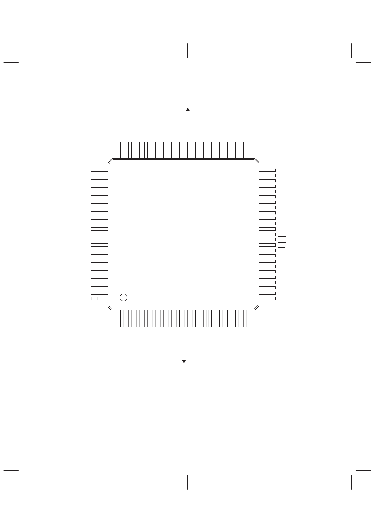
1.3 Terminal Assignments
76
77
78
79
80
81
82
83
84
85
86
87
88
89
90
91
92
93
94
95
96
97
98
99
100
50
49
48
47
46
45
44
43
42
41
40
39
38
37
36
35
34
33
32
31
30
29
28
27
26
12345678910111213141516171819202122232425
75747372717069686766656463626160595857565554535251
GND
DATA16
DATA17
DATA18
DATA19
DATA20
DATA21
DATA22
DATA23
GND
DATA24
DATA25
DATA26
DATA27
DATA28
DATA29
DATA30
DATA31
GND
ADDR0
ADDR1
ADDR2
ADDR3
Reserved
NTCLK
NTOUT
NTBIHIZ
GND
ISO
GND
LREQ
GND
SCLK
CTL0
CTL1
GNDD0D1D2D3D4D5D6D7
GND
CYST
CYDNE
GRFEMP
GND
GND
GND
CYCLEOUT
V
CC
CYCLEIN
GND
GND
RESET
GND
INT
WR
CA
CS
VCC+5V
BCLK
GND
ADDR7
ADDR6
ADDR5
ADDR4
V
CC
POWERON
RAMEZ
GND
GND
GND
GND
DATA0
DATA1
DATA2
DATA3
VCC+5V
DATA4
DATA5
DATA6
DATA7
GND
DATA8
DATA9
DATA10
DATA11
V
CC
DATA12
DATA13
DATA14
DATA15
V
CC
V
V
CC
CC
To Host
To PHY Layer
NOTES: A. Tie reserved terminals to GND.
TSB12LV01A
PZ PACKAGE
(TOP VIEW)
B. Bit 0 is the most significant bit (MSB).
V
CC
+5V
V
CC
+5V
Page 12
1–4
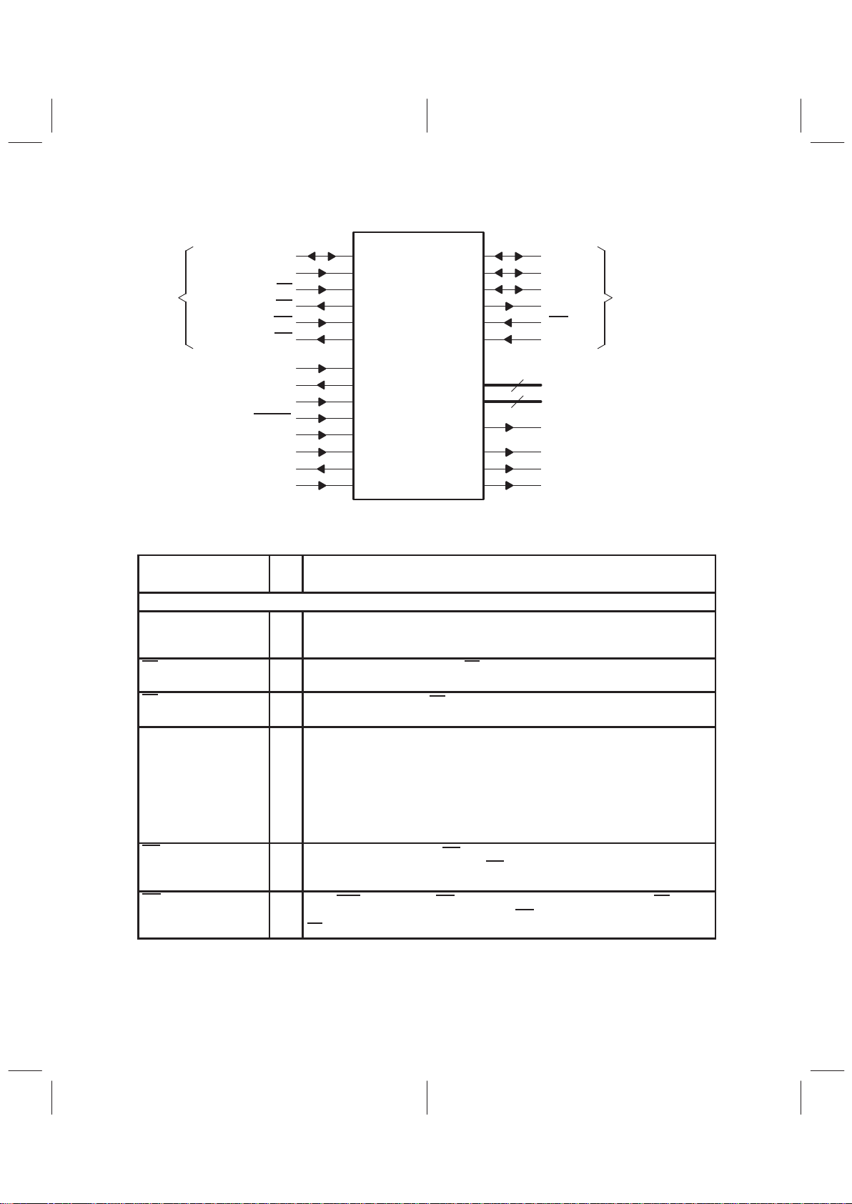
1.4 Terminal Functions
PHY Interface
D0 – D7
CTL0
CTL1
LREQ
ISO
SCLK
DATA0 – DATA31
ADDR0 – ADDR7
CS
CA
WR
INT
CYCLEIN
CYCLEOUT
BCLK
RESET
RAMEZ
V
CC
GND
Host
Bus
10
20
TSB12LV01A
NTCLK
NTOUT
NTBIHIZ
CYST
CYDNE
GRFEMP
POWERON
Figure 1–1. TSB12LV01A Terminal Functions
Table 1–1. Terminal Functions
TERMINAL
NAME NO.
I/O
DESCRIPTION
Host Bus Interface
ADDR0 –
ADDR7
22–25
27–30
I Address 0 through address 7. Host bus address bus bits 0 through 7 that address
the quadlet-aligned FIFOs and configuration registers. The two least significant
address lines, 6 and 7, must be grounded. Bit 0 is the most significant bit.
CA 35 O Cycle acknowledge (active low). CA is a TSB12L V01A control signal to the host bus.
When asserted (low), access to the configuration registers or FIFO is complete.
CS 34 I
Cycle start (active low). CS is a host bus control signal to initiate access to the
configuration registers or FIFO.
DATA0 –
DATA31
2–5
7–10
12–15
17–20
82–85
87–90
92–95
97–100
I/O Data 0 through 31. DATA is a host bus data bus bits 0 through 31. Bit 0 is the most
significant bit. Byte 0 is the most significant byte.
INT 37 O
Interrupt (active low). When INT is asserted (low), the TSB12L V01A notifies the host
bus that an interrupt has occurred. INT
is cleared when all the bits INT bits are
cleared in the INT register (or the mask is set false).
WR 36 I
Read/write enable. When WR is deasserted (high) in conjunction with CS, a read
from the TSB12LV01A is requested. When WR
is asserted (low) in conjunction with
CS
, a write to the TSB12LV01A is requested.
Page 13
1–5
Table 1–1. Terminal Functions (Continued)
TERMINAL
NAME NO.
I/O
DESCRIPTION
PHY Interface
CTL1, CTL0 62, 63 I/O Control 1 and control 0 of the PHY -link control bus. CTL1 and CTL0 indicate the four
operations that can occur in this interface (see Section 7 of this document or Annex
J of the IEEE 1394-1995 standard for more information about the four operations).
These terminals have bus holder functionality built in. When RESET
is asserted,
CTL0 and CTL1 are initialized to 0 (low) for one SCLK cycle and then released. The
bus holders then hold CTL0 and CTL1 at 0 (low) until a transition is driven.
D0 – D7 52–55
57–60
I/O Data 0 through data 7 of the PHY-link data bus. Data is expected on D0 – D1 for
100 Mbits/s packets, D0 – D3 for 200 Mbits/s, and D0 – D7 for 400 Mbits/s transfers.
These terminals have bus holder functionality built in. When RESET
is asserted,
D0 – D7 are initialized to 0 (low) for one SCLK cycle and then released. The bus
holders then hold D0 – D7 at 0 (low) until a transition is driven.
ISO 69 I
Isolation barrier (active low). ISO is asserted (low) when an isolation barrier is
present. This terminal only supports bus holder type isolation.
LREQ 67 O Link request. LREQ is a TSB12LV01A output that makes bus requests and access
requests to the PHY layer. On the first rising edge of SCLK when RESET
is asserted,
LREQ is driven to 0 (low).
POWERON 76 O Power on indicator to PHY interface. When active, POWERON has a clock output
with 1/16 of the BCLK frequency and indicates to the PHY interface that the
TSB12LV01A is powered. This terminal can be connected to the link power status
(LPS) terminal on the TI PHY devices to provide an indication of the LLC power
condition. When RESET
is asserted, POWERON is driven to 0 (low).
SCLK 65 I System clock. SCLK is a 49.152-MHz clock from the PHY, that generates the internal
24.576-MHz clock used internally in the TSB12L V01A.
Miscellaneous Signals
BCLK 32 I Bus clock. BCLK is the host bus clock used for the host-interface module of the
TSB12LV01A. It is asynchronous to SCLK.
CYCLEIN 42 I Cycle in. CYCLEIN is an optional external 8,000-Hz clock used to time the
isochronous cycle clock, and it should only be used when attached to the
cycle-master node. It is enabled by the cycle source bit and should be tied high when
not used.
CYCLEOUT 44 O Cycle out. CYCLEOUT is the version of the isochronous cycle clock used by the
TSB12LV01A. It is based on the internal timer controls and received cycle-start
messages.
CYDNE 49 O Status of CyDne bit. CYDNE indicates the value of the CyDne bit of the interrupt
register. This terminal is asserted for as long as the interrupt bit is assigned.
CYST 50 O Status of CySt bit. CYST indicates the value of the CySt bit of the interrupt register.
This terminal is asserted for as long as the interrupt bit is set.
Page 14
1–6
Table 1–1. Terminal Functions (Continued)
TERMINAL
NAME NO.
I/O
DESCRIPTION
GND 1, 11, 21,
31, 38, 40,
41, 45–47,
51, 61, 66,
68, 70,
78–81, 91
Ground reference
GRFEMP 48 O Status of Empty bit. This terminal is asserted for as long as the GRFEMP bit is set.
RAMEZ 77 I RAM 3-state enable. When RAMEZ is deasserted (low), FIFOs are enabled. When
RAMEZ is asserted, the FIFOs are 3-state outputs. (This is a manufacturing
test-mode condition and should be grounded under normal operating conditions.)
NTBIHIZ 71 I NAND-tree bidirectional 3-state output. When NTBIHIZ is deasserted (low), the
bidirectional I/Os operate in a normal state. When NTBIHZ is asserted (high), the
bidirectional I/Os are in the 3-state output mode. (This is a manufacturing
test-mode condition and should be grounded under normal operating conditions.)
NTCLK 73 I NAND clock input. The NAND-tree clock is used for VIH and VIL manufacturing
tests. (This input should be grounded under normal operating conditions.)
NTOUT 72 O NAND-tree output. This output should remain open under normal operating
conditions.
RESET 39 I Reset (active low). RESET is the asynchronous reset to the TSB12LV01A.
V
CC
6, 26, 43,
56, 74, 96
3.3-V ±5% power supplies
VCC+5V 16, 33
64, 86
5-V ±5% power supplies
Page 15
2–1
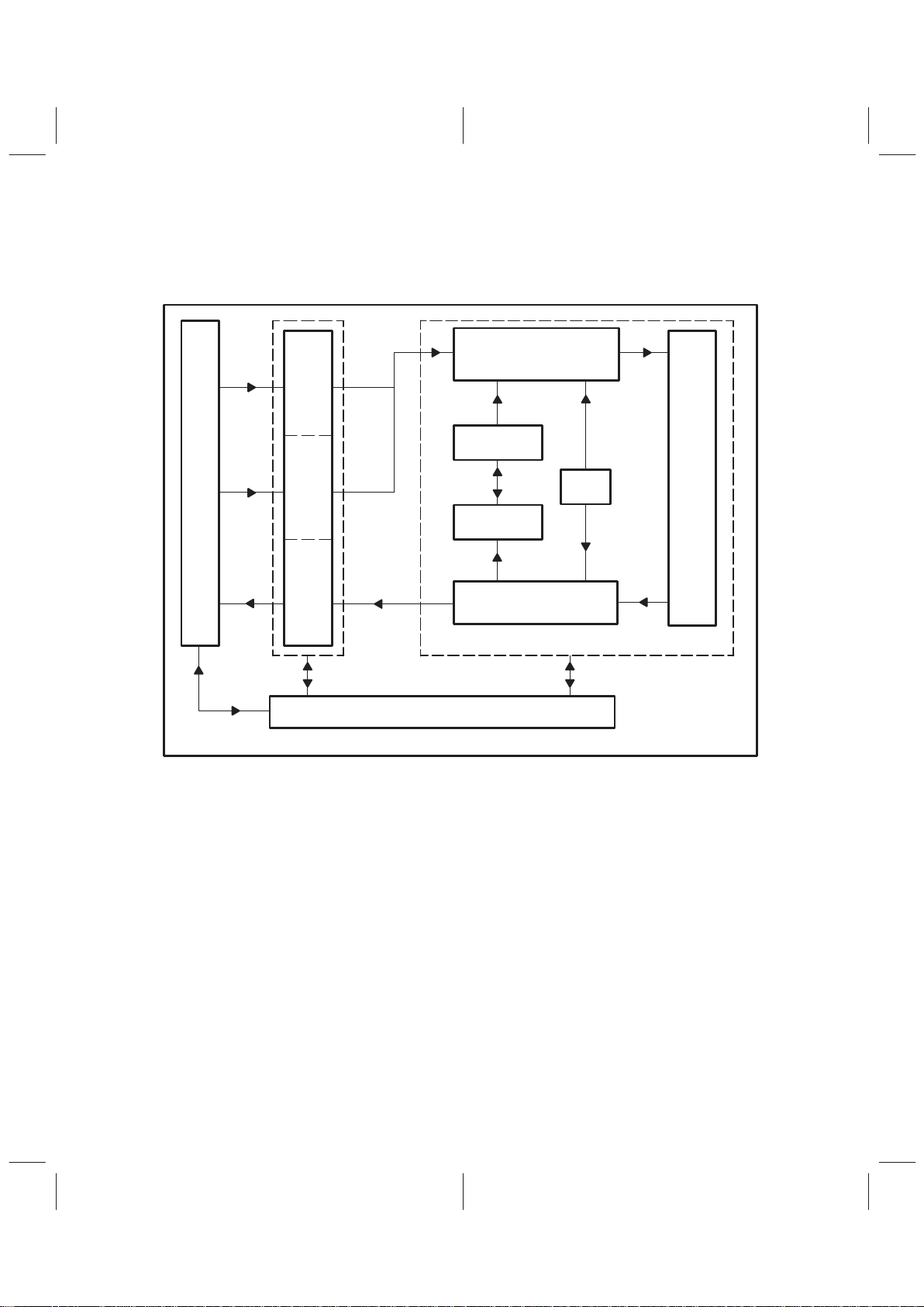
2 Architecture
2.1 Functional Block Diagram
The functional block architecture of the TSB12LV01A is shown in Figure 2–1.
Transmitter
Cycle Timer
Cycle Monitor
CRC
Receiver
Configuration Registers
GRF
ITF
ATF
P
h
y
s
i
c
a
l
I
n
t
e
r
f
a
c
e
H
o
s
t
I
n
t
e
r
f
a
c
e
Figure 2–1. TSB12LV01A Block Diagram
2.1.1 Physical Interface
The physical (PHY) interface provides PHY-level services to the transmitter and receiver . This includes gaining access to the serial bus, sending packets, receiving packets, sending and receiving acknowledge packets, and reading and writing PHY registers.
The PHY interface module also interfaces to the PHY chip and conforms to the PHY -link interface specification described in Annex J of the IEEE 1394-1995 standard (refer to Section 7 of this document for more information).
2.1.2 Transmitter
The transmitter retrieves data from either the ATF or the ITF and creates correctly formatted serial-bus
packets to be transmitted through the PHY interface. When data is present at the ATF interface to the
transmitter, the TSB12LV01A PHY interface requests the serial bus and upon receiving a grant, sends a
packet. When data is present at the ITF interface to the transmitter, the TSB12L V01A arbitrates for the serial
bus during the next isochronous cycle. The transmitter autonomously sends the cycle-start packets when
the chip is the cycle master. The PHY interface provides PHY-level services to the transmitter and receiver.
This includes gaining access to the serial bus, sending packets, receiving packets, and receiving status from
the physical layer.
Page 16

2–2
2.1.3 Receiver
The receiver takes incoming data from the PHY interface and determines if the incoming data is addressed
to this node. If the incoming packet is addressed to this node, the CRC of the packet header is checked.
If the header CRC is good, the header is stored in the GRF. For block and isochronous packets, the
remainder of the packet is stored one quadlet at a time. The receiver places a status quadlet in the GRF
after the last quadlet of the packet is checked in the GRF . The status quadlet contains the error code for the
packet. The error code is the acknowledge code that was or could have been sent for that packet. For
broadcast packets that do not need an acknowledge packet, the error code is the acknowledge code that
would have been sent. This acknowledge code tells the transaction layer whether or not the data CRC is
good or bad. When the header CRC is bad, the header is flushed and the rest of the packet is ignored. Bad
packets are automatically flushed by the receiver.
When a cycle-start message is received, it is detected and the cycle-start message data is sent to the cycle
timer. The cycle-start messages can be placed in the GRF like other quadlet packets.
2.1.4 Transmit and Receive FIFOs
The TSB12LV01A contains two transmit FIFOs (ATF and ITF) and one receive FIFO (GRF). Each of these
FIFOs is one quadlet wide and their length is software selectable. These software-selectable FIFOs allow
customization of the size of each FIFO for individual applications. The sum of all FIFOs cannot be larger
than 512 quadlets. The transmit FIFOs are write only from the host bus interface, and the receive FIFO is
read only from the host bus interface. FIFO sizes must not be changed on the fly. All transactions must be
ignored and FIFOs cleared before changing the FIFO sizes.
An example of how to use software-adjustable FIFOs follows:
In applications where isochronous packets are large and asynchronous packets are small, the
implementers can set the ITF to a large size, 200 quadlets, and set the ATF to a smaller size, 100
quadlets.This means 212 quadlets are allocated to the GRF . Notice that the sum of all FIFOs is equal to 512
quadlets. Only the A TF size and the ITF size can be programmed, the remaining space is assigned to the
GRF.
2.1.5 Cycle Timer
The cycle timer is used by nodes that support isochronous data transfer. The cycle timer is a 32-bit
cycle-timer register. Each node with isochronous data-transfer capability has a cycle-timer register as
defined in the IEEE 1394-1995 standard. In the TSB12L V01A, the cycle-timer register is implemented in the
cycle timer and is located in IEEE-1212 initial register space at location 200h. It can also be accessed
through the host bus at address 14h. The cycle timer contains the cycle-timer register. The cycle-timer
register consists of three fields; cycle offset, cycle-count, and seconds count. The low-order 12 bits of the
timer are a modulo 3072 counter, which increments once every 24.576-MHz clock periods (or 40.69 ns).
The next 13 higher-order bits are a count of 8,000-Hz (or 125 µs) cycles, and the highest 7 bits count
seconds. The timer can be disabled using the cycle-timer-enable bit in the control register.
The cycle timer has two possible sources. The first cycle-source option is when the cycle source (CySrc)
bit in the configuration register is set, then the CYCLEIN input causes the cycle-count field to increment for
each positive transition of the CYCLEIN input (8 kHz) and the cycle offset resets to all zeros. CYCLEIN
should only be the source when the node is cycle master. When the cycle-count field increments,
CYCLEOUT is generated.
The second cycle-source option is when the CySrc bit is cleared. In this state, the cycle-offset field of the
cycle-timer register is incremented by the internal 24.576-MHz clock. The cycle timer is updated by the
reception of the cycle-start packet for the noncycle master nodes. Each time the cycle-offset field rolls over ,
the cycle-count field is incremented and the CYCLEOUT signal is generated. The cycle-offset field in the
cycle-start packet is used by the cycle-master node to keep all nodes in phase and running with a nominal
isochronous cycle of 125 µs.
Page 17

2–3
The CTCLEOUT signal indicates whenever the cycle-count field of the cycle timer register increments.
Therefore, for a cyclemaster node CYCLEOUT indicates that it is time to send a cycle-start packet. And,
on noncyclemaster nodes, CYCLEOUT indicates that it is time to expect a cycle-start packet. The cycle-start
interrupt bit is set when the cycle-start packet is sent from the cyclemaster node or received by a
noncyclemaster node.
2.1.6 Cycle Monitor
The cycle monitor is only used by nodes that support isochronous data transfer. The cycle monitor observes
chip activity and handles scheduling of isochronous activity. When a cycle-start message is received or sent,
the cycle monitor sets the cycle-started interrupt bit. It also detects missing cycle-start packets and sets the
cycle-lost interrupt bit when this occurs. When the isochronous cycle is complete, the cycle monitor sets the
cycle-done-interrupt bit. The cycle monitor instructs the transmitter to send a cycle-start message when the
cycle-master bit is set in the control register.
2.1.7 Cyclic Redundancy Check (CRC)
The CRC module generates a 32-bit CRC for error detection. This is done for both the header and data. The
CRC module generates the header and data CRC for transmitting packets and checks the header and data
CRC for received packets. See the IEEE 1394-1995 standard for details on the generation of the CRC.
NOTE:This is the same CRC used by the IEEE802 LANs and the X3T9.5 FDDI.
2.1.8 Internal Registers
The internal registers control the operation of the TSB12LV01A.
2.1.9 Host Bus Interface
The host bus interface allows the TSB12LV01A to be easily connected to most host processors. This host
bus interface consists of a 32-bit data bus and an 8-bit address bus. The TSB12LV01A utilizes cycle-start
and cycle-acknowledge handshake signals to allow the local bus clock and the 1394 clock to be
asynchronous to one another. The TSB12LV01A is interrupt driven to reduce polling.
Page 18

2–4
Page 19

3–1
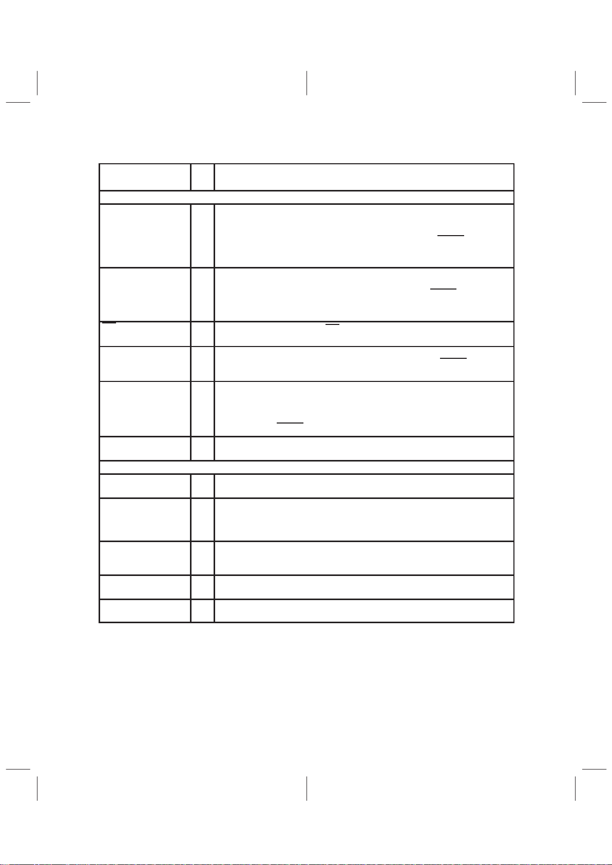
3 Internal Registers
3.1 General
The host-bus processor directs the operation of the TSB12LV01A through a set of registers internal to the
TSB12L V01A itself. These registers are read or written by asserting CS
with the proper address on ADDR0
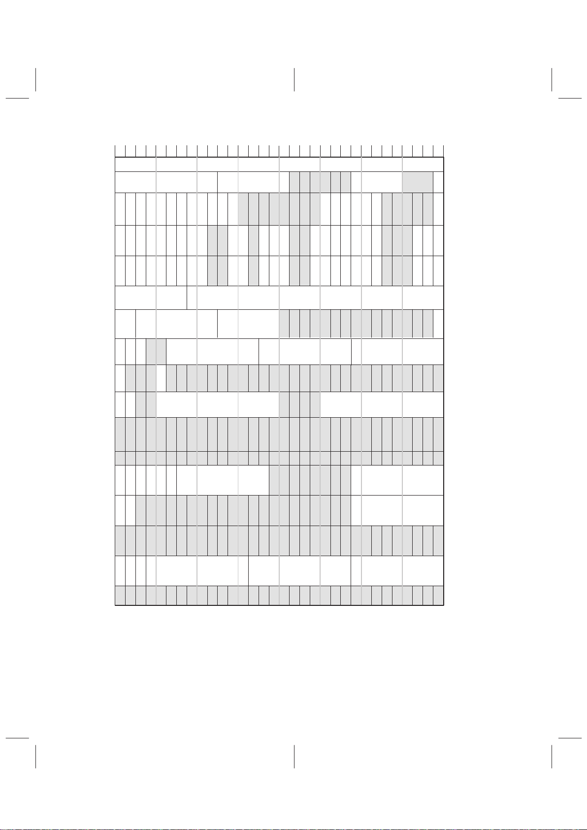
– ADDR7 and asserting or deasserting WR depending on whether a read or write is needed. Figure 3–1 lists
the register addresses; subsequent sections describe the function of the various registers.
3.2 Internal Register Definitions
The TSB12LV01A internal registers control the operation of the TSB12LV01A. The bit definitions of the
internal registers are shown in Figure 3–1 and are described in subsections 3.2.1 through 3.2.12.
There are three modes to access the internal TSB12LV01A registers; normal mode, quick mode, and burst
mode. The registers from address 00h to 2Ch are accessed using normal mode as shown in Figures 6–2
and 6–3.
The registers 30h, 34h, 3Ch, and C0h may be accessed using quick mode reads as shown in Figure 6–5.
The registers 30h and 80h through 9Ch may be accessed using quick mode writes as shown in Figure 6–4.
NOTE:
The protocols for normal mode and quick mode are exactly the same. The only
difference being that quick mode simply returns CA
quicker.
The registers 84h, 8Ch, 94h, 9Ch, A0h, and B0h may be accessed using burst mode writes as shown in
Figure 6–6.
The register C0h may be accessed using burst mode reads as shown in Figure 6–7.
Page 20
3–2
0 1 2 3 4 5 6 7 8 9 10 11 12 13 14 15 16 17 18 19 20 21 22 23 24 25 26 27 29 30 31
00h
Interrupt
CmdRst
ENSpRdPhy
TxlEn
ATAck
Int IdVal
PhInt RxSId
PhRRx
TxRdy
RxDta
PhRst
WrPhy
regRW
TxAEn
RxAEn
RstRx
RxlEn
AckCen
RstTx
ITBadF
ATBadF
SntRj
HdrEr
TCErr
CyDne
CySec
CySt
CyPnd
CyLst
CArbFl
IArbFl
Full
Empty
Full
Empty
Empty
cd
Control
PhyRgAd PhyRxAd
Version
Node
Address
Control
FIFO
Control
Cycle
Timer
Interrupt
Mask
Isoch Port
Number
Diagnostics
Phy Chip
Access
Reserved
Reserved
ATF Status
(R/W)
ITF Status
(Read Only)
Reserved
GRF Status
(Read Only)
Reserved
CyTEn
CyMas
CySrc
IRP1En
IRP2En
04h
08h
0Ch
10h
14h
18h
1Ch
20h
24h
28h
2Ch
30h
34h
38h
3Ch
40h
28
TrgEn
FhBad
7 Bits
IR Port1
Seconds Count
BsyCtrl
Bus Number
TAG2
TAG1
Rollover @ 8000
Cycle Count
13 Bits Rollover @ 3072 12 Bits
IR Port2
Node Number
Version
PhyRgData
Revision
Cycle Offset
PhyRxData
ATFSpaceCount
ITFSpaceCount
WriteCount
Root
AckV
3031-3042
RAl
RcvCyst
SIDCom
FrGp
ArbGp
CyTm0
MonTag
ClrGRF
Trigger Size ATFSize ITFSize
ClrITF
CLrATF
ConErr
AdrClr
RAMTest
AdrCounter
PacCom
GRFTotalCnt GRFSize
CmdRst
Int
PhInt
PhRRx
TxRdy
RxDta
PhRst
ITBadF
ATBadF
SntRj
HdrEr
TCErr
CyDne
CySec
CySt
CyPnd
CyLst
CArbFl
IArbFl
SIDCom
FrGp
ArbGp
CyTm0
ACKRCVACKRCV
NOTE A: All gray areas (bits) are reserved bits.
Figure 3–1. Internal Register Map
Page 21
3–3
3.2.1 Version/Revision Register (@00h)
The version/revision register allows software to be written that supports multiple versions of the high-speed
serial-bus link-layer controllers. This register is at address 00h and is read only. The initial value is
3031_3042h.
Table 3–1. Version/Revision Register Field Descriptions
BITS ACRONYM FUNCTION NAME DESCRIPTION
0–15 Version Version Version of the
TSB12LV01A
16–31 Revision Revision Revision of the
TSB12LV01A
3.2.2 Node-Address/Transmitter Acknowledge Register (@04h)
The node-address/transmitter acknowledge register controls which packets are accepted/rejected, and it
presents the last acknowledge received for packets sent from the ATF. This register is at offset 04h. The
bus number and node number fields are read/write. The AT acknowledge (A T Ack) received is normally read
only. Setting the regRW bit in the diagnostic register makes these fields read/write. The initial value is
FFFF_0000h. The node number field and the root field are automatically updated by every PHY register 0
status transfer to the TSB12LV01A.
Table 3–2. Node-Address/Transmitter Acknowledge Register Field Descriptions
BITS ACRONYM FUNCTION NAME DESCRIPTION
0–9 BusNumber Bus number BusNumber is the 10-bit IEEE 1212 bus number that the
TSB12LV01A uses with the node number in the SOURCE
address for outgoing packets and to accept or reject incoming
packets. The TSB12LV01A always accepts packets with a bus
number equal to 3FFh.
10–15 NodeNumber Node number NodeNumber is the 6-bit node number that the TSB12LV01A
uses with the bus number in the source address for outgoing
packets and to accept or reject incoming packets. The
TSB12LV01A always accepts packets with the node address
equal to 3Fh. After bus reset, the node number is automatically
set to the node’s Physical_ID by a PHY register 0 transfer.
16
†
Root Root If Root =1 this node is root, read only
17–22
‡
Reserved Reserved Reserved
23–27
‡
ATAck Address transmitter
acknowledge
received
ATAck is the last acknowledge received by the transmitting
node in response to a packet sent from the asynchronous
transmit-FIFO.
ATAck=0_XXXX the low order 4 bits present normal ack code
receive from the receiving node.
ATAck=1_0000 an acknowledge timeout occured
ATAck=1_0011 ack packet error (ack parity error, or ack
pPending too long or ack pending too short)
28–30 Reserved Reserved Reserved
†
This bit is new to the TSB12LV01A and does not exist in the TSB12C01A.
‡
The bit number of these bits is different than the bit number listed for the TSB12C01A.
Page 22
3–4
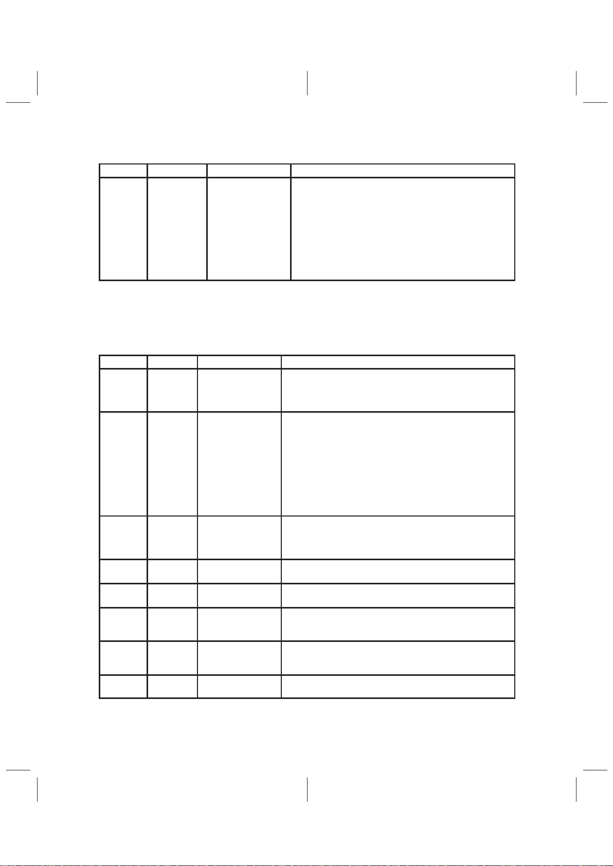
Table 3–2. Node-Address/Transmitter Acknowledge Register Field Descriptions (Continued)
BITS ACRONYM FUNCTION NAME DESCRIPTION
31
†
AckV Acknowledge valid Whenever an ack packet is received, AckV alid is set to 1. After
the node-address/transmitter acknowledge register is read,
AckValid is automatically reset to 0. This bit is also used to
indicate abitration failure. If a non-broadcast asynchronous
packet is in the ATF ready to transmit and a TxRdy interrupt
occurs, and AckValid is 0, this indicates no ack packet was
received and no ack time-out occured. The packet is still in the
ATF and the TSB12LV01A automatically arbitrates for the bus
again. Under normal conditions AckValid=0 means ATAck
contains last received ack code information.
†
This bit is new to the TSB12LV01A and does not exist in the TSB12C01A.
3.2.3 Control Register (@08h)
The control register dictates the basic operation of the TSB12LV01A. This register is at address 08h and
is read/write. The initial value is 0000_0000h.
Table 3–3. Control-Register Field Descriptions
BITS ACRONYM FUNCTION NAME DESCRIPTION
0 IdVal ID valid When IdVal is set, the TSB12LV01A accepts packets addressed
to the IEEE 1212 address set (Node Number) in the node-address
register. When IdVal is cleared, the TSB12LV01A accepts only
broadcast packets.
1 RxSId Received self-ID
packets
When RxSId is set, the self-identification packets generated by
phy chips during bus initialization are received and placed into the
GRF as a single packet. Each self-identification packet is
composed of two quadlets, where the second quadlet is the logical
inverse of the first. If ACK (4 bits) equals 1h, then the data is good.
If ACK equals Dh, then the data is wrong. When the RxSld is set
to 1, it also receives and places Link-on-packet and PHY
Configuration packet into the GRF. For Link-on-packet and PHY
Configuration packet only the first quadlet of each packet is stored
in the GRF.
2 BsyCtrl Busy control When this bit is set, this node sends an ack_busy_x acknowledge
in response to all received non-broadcast asynchronous packets.
When this bit is clear, this node sends ack_busy_x acknowledge
only if the GRF is full.
3
†
RAI Received all isochro-
nous packets
If RAI = 1 , RxIEn = 1, TSB12LV01A receives all Isochronous
packets and stores in the GRF.
4
†
RcvCySt Receive cycle start If RcvCySt = 1, it stores the received cycle start packet in the
GRF.
5 TxAEn Transmitter enable When TxAEn is cleared, the transmitter does not arbitrate or send
asynchronous packets. After bus reset, TxAEn is cleared since
the node number may have changed.
6 RxAEn Receiver enable When RxAEn is cleared, the receiver does not receive any
asynchronous packets. After bus reset, RxAEn is cleared since
the node number may have changed.
7
†
TxIEn Transmit
isochronous enable
When TxIEn is cleared, the transmitter does not arbitrate to send
isochronous packets
†
This bit is new to the TSB12LV01A and does not exist in the TSB12C01A.
Page 23

3–5
Table 3–3. Control-Register Field Descriptions (Continued)
BITS ACRONYM FUNCTION NAME DESCRIPTION
8
†
RxIEn Receive
isochronous
enable
When RxIEn is cleared, the receiver does not receive isochronous
packets.
9
†
AckCEn Ack complete
enable
When AckCEn is set, the 12LV01A sends the Ack_complete code to the
transmit node for receiving a non-broadcast write request packet if
GRF is not full and there is no error in the packet. When AckCEn is
cleared, TSB12LV01A sends an Ack_pending code for the above
condition.
10 RstTx Reset transmitter When RstTx is set, the entire transmitter resets synchronously. This bit
clears itself.
11 RstRx Reset receiver When RstRx is set, the entire receiver resets synchronously. This bit
clears itself.
12–19†Reserved Reserved Reserved
20 CyMas Cycle master When CyMas is set and the TSB12LV01A is attached to the root phy,
the cyclemaster function is enabled. When the cycle_count field of the
cycle timer register increments, the transmitter sends a cycle-start
packet. This bit is not cleared upon bus reset. When another node is
selected as root during a bus reset, the transaction layer in the now
nonroot TSB12L V01A node must clear this bit and the transaction layer
in the TSB12LV01A node selected as root must set this bit.
21 CySrc Cycle source When CySrc is set, the cycle_count field increments and the
cycle_offset field resets for each positive transition of CYCLEIN. When
CySrc is cleared, the cycle_count field increments when the
cycle_offset field rolls over.
22 CyTEn Cycle-timer enable When CyTEn is set, the cycle_offset field increments. This bit must be
set to transmit cycle start packets for cycle master node. This bit must
be set to receive or transmit isochronous packets.
23 TrgEn Trigger size func-
tion enable
If TrgEn is set, the receiver partitions the received packet into trigger
size blocks. Trigger size is defined in FIFO Control register. For example: if trigger size=8 and total received packet size (excluding header
CRC and data CRC)=20 quadlets. The receiver creates 3 blocks of
data in GRF. Each block starts with a packet token quadlet to indicate
how many quadlets follow this packet token. The first and the second
block have 9 quadlets (including the packet token quadlet). The third
block has 5 quadlets(including a packet token quadlet). Each block triggers one RxDta interrupt. The purpose of the trigger size function is to
allow the receiver to receive a packet larger than GRF size and host bus
can read the received data when each block is available without waiting
till the whole packet is loaded into GRF, so the host bus latency is reduced.
24 IRP1En IR port 1 enable When IRP1En is set, the receiver accepts isochronous packets when
the channel number matches the value in the IR Port1 field.
25 IRP2En IR port 2 enable When IRP2En is set, the receiver accepts isochronous packets when
the channel number matches the value in the IR Port2 field.
26–30 Reserved Reserved Reserved
31
†
FhBad Flush bad packets When the FhBad is set, the receiver flushes any received bad packets
(including a partial packet due to GRF full)and it does not generate a
RxDta interrupt. When FhBad is set, it disables the TrgEn function.
†
This bit or bits are new to the TSB12LV01A and do not exist in the TSB12C01A.
Page 24

3–6
3.2.4 Interrupt and Interrupt-Mask Registers (@0Ch, @10h)
The interrupt and interrupt-mask registers work in tandem to inform the host bus interface when the state
of the TSB12LV01A changes. The interrupt register is at address 0Ch. The interrupt mask register is at
address 10h. The interrupt mask register is read/write. Its initial value is 0000_0000h. When regRW is
cleared to 0, the interrupt register (except for the Int bit) is cleared. When regRW (in diagnostics register
@20h) is set to 1, the interrupt register (including the Int bit) is read/write. Its initial value is 1000_0000h.
The interrupt bits all work the same. For example, when a phy interrupt occurs, the PhInt bit is set. If the
PhIntMask bit is set, the Int bit is set. If the IntMask is set, the INT signal is asserted. The logic for the interrupt
bits is shown in Figure 3–2. Table 3–4 defines the interrupt and interrupt-mask register field descriptions.
As shown in Figure 3–2, the INT bit is the OR of interrupt bits 1 – 31. When all the interrupt bits are cleared,
INT equals 0. When any of the interrupt bits are set, INT is set to 1, even if the INT bit was just cleared.
Set
Clear
Clk
PhInt Bit
Interrupt Bit (INT)
Other
Interrupts
Interrupt Bit
IntMask Bit
PhInt Bit
PhIntMask Bit
INT
DATA (01)
CS
WR
PhInt Source
SCLK
Q
Figure 3–2. Interrupt Logic Diagram Example
Page 25

3–7
Table 3–4. Interrupt- and Mask-Register Field Descriptions
BITS ACRONYM FUNCTION NAME DESCRIPTION
0 Int Interrupt Int contains the value of all interrupt and interrupt mask bits ORed
together.
1 PhInt Phy chip interrupt When PhInt is set, the phy chip has signaled an interrupt through the
pPhy interface.
2 PhyRRx Phy register
information received
When PhyRRx is set, a register value has been transferred to the phy
chip access register (offset 24h) from the phy interface.
3 PhRst Phy reset started When PhRst is set, a phy-layer reconfiguration has started (1394 bus
reset).
4
†
SIDComp Self ID complete When SIDComp is set, a complete bus reset process is finished. If the
RxSId bit (bit 1) of the control register (08h) is set, the GRF contains
all received self-ID packets.
5 TxRdy Transmitter ready When TxRdy is set, the transmitter is idle and ready. When TxRdy is
set to 1 and AckV (bit 31 of node address register) remains 0 for a
non-broadcast asynchronous packet, the transmitter fails arbitration
and arbitrates for the bus again when the bus is idle.
6 RxDta Receiver has data In normal mode and when set, RxDta indicates that the receiver has
accepted a block of data(if TrgEn=0, a block of data means a packet)
into the GRF interface. However, during the self-ID portion of a bus
reset, this bit is set after the bus reset process is done.
7 CmdRst Command reset
received
When CmdRst is set, the receiver has been sent a quadlet write
request addressed to the RESET_START CSR register.
8 ACKRCV Receive ACK
Packet Interrupt
This interrupt is triggered when an acknowledge is received or a
timeout has occurred after an asynchronous packet is sent. To enable this register, the mask interrupt should be set to 1.
9–10 Reserved Reserved Reserved
11†ITBadF Bad pPacket
formatted in ITF
When ITBadF is set, the transmitter has detected invalid data at the
isochronous transmit-FIFO interface.
12†ATBadF Bad packet
formatted in ATF
When ATBadF is set, the transmitter has detected invalid data at the
asynchronous transmit-FIFO interface. If the first quadlet of a packet
is not written to the ATF_First or ATF_First & Update, the transmitter
enters a state denoted by an ATBadF interrupt. An underflow of the ATF
also causes an ATBadF interrupt. If this state is entered, no
asynchronous packets can be sent until the ATF is cleared by way of
the CLR ATF control bit. Isochronous packets can be sent while in this
state.
13 Reserved Reserved Reserved
14 SntRj Busy acknowledge
sent by receiver
SntRj is set when there is a GRF overflow. The receiver is then forced
to send a busy acknowledge to a packet addressed to this node
because the GRF overflowed.
15 HdrEr Header error When HdrEr is set, the receiver detected a header CRC error on an
incoming packet that may have been addressed to this node. The
packet will be discarded.
16 TCErr Transaction code
error
When TCErr is set, the transmitter detected an invalid transaction code
in the data at the transmit FIFO interface.
17–18 Reserved Reserved Reserved
19†CyTmOut Cycle timer out Isochronous cycle lasts more than 125 µs.
†
This bit is new to the TSB12LV01A and does not exist in the TSB12C01A.
Page 26

3–8
Table 3–4. Interrupt- and Mask-Register Field Descriptions (Continued)
BITS ACRONYM FUNCTION NAME DESCRIPTION
20 CySec Cycle second
incremented
When CySec is set, the cycle-second field in the cycle-timer register
is incremented. This occurs approximately every second when the
cycle timer is enabled.
21 CySt Cycle started When CySt is set, the transmitter has sent or the receiver has received
a cycle-start packet.
22 CyDne Cycle done When CyDne is set, a subaction gap has been detected on the bus after
the transmission or reception of a cycle-start packet. This indicates that
the isochronous cycle is over.
23 CyPnd Cycle pending When CyPnd is set, the cycle-timer offset is set to 0 (rolled over or
reset) and remains set until the isochronous cycle ends.
24 CyLst Cycle lost When CyLst is set, the cycle timer has rolled over twice without the
reception of a cycle-start packet. This occurs only when this node is not
the cycle master.
25 CArbFI Cycle arbitration
failed
When CArbFI is set, the arbitration to send the cycle-start packet failed.
26–28 Reserved Reserved Reserved
29†ArbGp Arbitration gap Arbitration gap occured.
30†FrGp Subaction gap Subaction gap occured.
31 IArbFI Isochronous
arbitration failed
When IArbFI is set, the arbitration to send an isochronous packet failed.
†
This bit is new to the TSB12LV01A and does not exist in the TSB12C01A.
3.2.5 Cycle-Timer Register (@14h)
The cycle-timer register contains the seconds_count, cycle_count and cycle_offset fields of the cycle timer.
The register is at address 14h and is read/write. This field is controlled by the cycle master, cycle source,
and cycle timer enable bits of the control register. Its initial value is 0000_0000h.
Table 3–5. Cycle-Timer Register Field Descriptions
BITS ACRONYM FUNCTION NAME DESCRIPTION
0–6 seconds_count Seconds count 1-Hz cycle-timer counter
7–19 cycle_count Cycle count 8,000-Hz cycle-timer counter
20–31 cycle_offset Cycle offset 24.576-MHz cycle-timer counter
Page 27

3–9
3.2.6 Isochronous Receive-Port Number Register (@18h)
The isochronous receive-port number register controls which isochronous channels are received by this
node. If RAI of Control register is set, this register value is don’t care since all channels are received. This
register is at address 18h. The register is read/write, and its initial value is 0000_0000h.
Table 3–6. Isochronous Receive-Port Number Register Field Descriptions
BITS ACRONYM FUNCTION NAME DESCRIPTION
0–1†TAG1 Tag bit 1 Isochronous data format tag. See IEEE 1394-1995 6.2.3 and
IEC 61883.
2–7 IRPort1 Isochronous receive
TAG bits and port 1
channel number
IRPort1 contains the channel number of the isochronous packets the
receiver accepts when IRP1En is set. See Table 4–5 and Table 4–6
for more information.
8–9†Tag2 Tag bit 2 Isochronous data format tag. See IEEE 1394-1995 6.2.3
10–15 IRPort2 Isochronous receive
TAG bits and port 2
channel number
IRPort2 contains the channel number of the isochronous packets the
receiver accepts when IRP2En is set (bits 8 and 9 are reserved as
TAG bits). See Table 4–5 and Table 4–6 for more information.
16–30 Reserved Reserved Reserved
31†Mon Tag Tag enable When set, it enables the tag bit comparison. If both Tagx and IR-
PORTx match for port number x, the matching receive Iso packet
is stored in the GRF.
†
This bit or bits are new to the TSB12LV01A and do not exist in the TSB12C01A.
3.2.7 FIFO Control Register (@1Ch)
‡
FIFO Control register is used to clear ATF, ITF, GRF and set up the trigger size for the trigger-size function.
ATF size and ITF size are all in the quadlet. GRF size = 512–(ATF Size)– (ITF size)
Table 3–7. Node-Address/ Transmitter Acknowledge Register Field Descriptions
BITS ACRONYM FUNCTION NAME DESCRIPTION
0 ClrATF Clear asynchronous
transfer FIFO
Writing 1 to this bit automatically clears the A TF to 0. This bit is
self clearing.
1 ClrITF Clear isochronous
transfer FIFO
Writing 1 to this bit automatically clears the ITF to 0. This bit is
self clearing.
2 ClrGRF Clear general receive
FIFO
Writing 1 to this bit automatically clears the GRF to 0. This bit is
self clearing.
3–4 Reserved Reserved Reserved
5–13 Trigger Size Trigger size Trigger size is used to split a big receive packet into several
smaller blocks of data, so the host bus does not have to wait the
whole packet cycle before it can read the GRF , When TrgEn=0
or FhBad=1 in the control register, trigger size is don’t care. The
trigger size is specified in quadlets.
14–22 ATFSize Asynchronous trans-
mitter FIFO size
ATFSize allocates ATF size in the quadlets. The limitations for
ATFSize are ATFSise<=512 and (ATFSize+ITFSize) <=512.
23–31 ITFSize Isochronous trans-
mitter FIFO size
Same as above except for ITF
‡
This register is new to the TSB12LV01A and does not exist in the TSB12C01A.
Page 28

3–10
3.2.8 Diagnostic Control Register (@20h)
The diagnostic control and status register allows for the monitoring and control of the diagnostic features
of the TSB12LV01A. The register is at address 20h. The regR W and enable snoop bits are read/write. When
regRW is cleared, all other bits are read only. When regRW is set, all bits are read/write. Its initial value is
0000_0000h.
Table 3–8. Diagnostic Control and Status-Register Field Descriptions
BITS ACRONYM FUNCTION NAME DESCRIPTION
0 ENSp Enable snoop When ENSp is set, the receiver accepts all packets on the bus
regardless of address or format. The receiver uses the snoop data
format defined in Section 4.4.
1–3†Reserved Reserved Reserved
4 regR/W Register read/write
access
When regR/W is set, most registers are fully read/write.
5–31†Reserved Reserved Reserved
†
This bit or bits are new to the TSB12LV01A and do not exist in the TSB12C01A.
3.2.9 Phy-Chip Access Register (@24h)
The phy-chip access register allows access to the registers in the attached phy chip. The most significant
16 bits send read and write requests to the phy-chip registers. The least significant 16 bits are for the phy
chip to respond to a read request sent by the TSB12LV01A. The phy-chip access register also allows the
phy interface to send important information back to the TSB12LV01A. When the phy interface sends new
information to the TSB12L V01A, the phy register-information-receive (PhyRRx) interrupt is set. The register
is at address 24h and is read/write. Its initial value is 0000_0000h. All gap counts (set in the phy device
registers) on all nodes of a 1394 bus must be identical. This can be accomplished by using the phy
configuration packets to set a specific gap count or by using two bus resets, which resets the gap counts
to the default 3Fh. See Section 4.6 for the format of the phy configuration packets.
Table 3–9. Phy-Chip Access Register
BITS ACRONYM FUNCTION NAME DESCRIPTION
0 RdPhy Read phy-chip
register
When RdPhy is set, the TSB12LV01A sends a read register request
with address equal to phyRgAd to the phy interface. This bit is cleared
when the request is sent.
1 WrPhy Write phy-chip
register
When WrPhy is set, the TSB12LV01A sends a write register request
with an address equal to phyRgAd on to the phy interface. This bit is
cleared when the request is sent.
2–3 Reserved Reserved Reserved
4–7 PhyRgAd Phy-chip-register
address
PhyRgAd is the address of the phy-chip register that is to be accessed.
8–15 PhyRgData Phy-chip-register
data
PhyRgData is the data to be written to the phy-chip register indicated
in PhyRgAd.
16–19 Reserved Reserved Reserved
20–23 PhyRxAd Phy-chip-register-
received address
PhyRxAd is the address of the register from which PhyRxData came.
24–31 PhyRxData Phy-chip-register-
received data
PhyRxData contains the data from register addressed by PhyRxAd.
Page 29

3–11
3.2.10 Asynchronous Transmit-FIFO (ATF) Status Register (@30h)
The ATF status register allows access to the registers that control or monitor the ATF. The register is at
address 30h. All the FIFO flag bits are read only, and the FIFO control bits are read/write. Its initial value
is 0000_0000h. This register provides RAM test mode control and status signals.
Table 3–10. ATF Status Register
BITS ACRONYM FUNCTION NAME DESCRIPTION
0 Full ATF full flag When Full is set, the FIFO is full. Write operations are ignored.
1
†
Empty ATF–empty flag When Empty is set, the FIFO is empty.
2
†
ConErr Control bit error Each location in the FIFO contains 33-bit data, the MSB is called the
Control bit, which is used to indicate the first quadlet of each packet
for ATF and ITF . In the GRF the control bit is used to indicate whether
the low order 32 bits contain a packet token. If control bit is 1, it indicates that the low order bits at that location are the first quadlet of the
packet in ATF or ITF, or a packet token in GRF. During RAM test
mode, the entire FIFO becomes a RAM. Control bits can be verified
indirectly. If ConErr is1, read value of control bit does not match write
value, which is defined by control (bit 4 of ATF status register). ConErr is clear to 0 by writing 1 to AdrClr or 0 to RAM test.
3
†
AdrClr Adder clear control Set AdrClr to 1 to clear AdrCounter and ConErr to 0, during the next
RAM access. The RAM test mode accesses location 0. AdrClr clears
itself to 0.
4
†
Control Control bit The value of control bit is used to relate the MSB of access RAM
location in RAM test mode. For RAM test mode WRITE– control bit
value concatenated with DATA0 – DATA31, writes to the location
pointed by the AdrCounter. For RAM test mode READ– the read
location is pointed to by the current AdrCounter. The read Control
counter bit is compared with Control bit (bit 4) of ATF status register ,
if it does not match, it sets ConErr to1.
5
†
RAMTest Ram test mode When RAM test is set to 1, all FIFO function are disabled. Write to or
read from address 80h writes to or reads from the location pointed to
by AdrCounter. After each write or read, AdrCounter is incremented
by 1. AdrCounter address range is from 0 to 511. For normal FIFO
operation , clear RAMTest to 0,and AdrClr, control, AdrCounter are
don’t care.
6–14†AdrCounter Address counter Gives the address location
15–22†Reserved Reserved Reserved
23–31†ATFSpace-
Count
ATF space count in
quadlets
ATF available space for loading next packet into ATF . If A TFSpace Count is larger than the next packet, then the software can burst
write the next packet into ATF. It only requires two host bus transactions: One ATF Status read and one burst write to ATF
†
This bit or bits are new to the TSB12LV01A and do not exist in the TSB12C01A.
Page 30

3–12
3.2.11 ITF Status Register (@34h)
The ITF status register allows access to the registers that control or monitor the ITF. The register is at
address 34h. All the FIFO flag bits are read only, and the FIFO control bits are read/write. Its initial value
is 0000_0000h.
Table 3–11. ITF Status Register
BITS ACRONYM FUNCTION NAME DESCRIPTION
0 Full ITF full flag When Full is set, the FIFO is full and all writes are ignored.
1
†
Empty Empty When Empty is set, ITF is empty.
2–22†Reserved Reserved Reserved
23–31†ITFSpace
Count
ITF space count in
quadlets
ITF available space for loading the next packet to the ITF. If
ITFSpaceCount is larger than the next packet quadlet, then the
software can burst write the next packet into ITF . It only requires two
host bus transactions: One ITF Status read and one burst write to
ITF
†
This bit or bits are new to the TSB12LV01A and do not exist in the TSB12C01A.
3.2.12 GRF Status Register (@3Ch)
The GRF status register allows access to the registers that control or monitor the GRF. The register is at
address 3Ch. All the FIFO flag bits are read only, and the FIFO control bits are read/write. Its initial value
is 0000_0000h.
Table 3–12. GRF Status Register
BITS ACRONYM FUNCTION NAME DESCRIPTION
0
†
Empty GRF empty flag When Empty is set, the GRF is empty.
1
†
cd GRF controller bit If cd is 1, a packet token is on the top of GRF. The next GRF read
returns the packet token.
2
†
PacCom Packet complete When cd=1 and PacComp=1 then the next block of data from the
GRF is the last one for the packet. When cd=1 and PacComp=0,
then the next block of data from the GRF is just one block of the
current receive packet.
If the trigger size function is disabled or flush bad packet function is
enabled, cd=1 and PacComp is 1. This means each received packet
only contains one block of GRF data. When cd=0 PacCom is not
valid.
3–12†GRFTotal
Count
Total GRF data count
stored in quadlet
GRF stored data count which includes all stored received packets
and internally-generated packet tokens.
13–22†GRFSize GRF size GRF Size=512–(ATFSize+ITFSize)
GRF Size is total assigned space for GRF
23–31†WriteCount Received data
quadlet count of next
block in GRF
This number is valid when cd bit is 1. It indicates the received data
quadlet count of next block. Write count also contains the packet
token. The packet token is always stored on the top of each receive
data block to provide status report, so software can burst read the
next block from GRF.
For the case of disable trigger size function or enable flush bad
receive packets:
To read each received packet from GRF, first read GRF status
register and make sure cd=1 so the packet token is on the top of
GRF . Next do burst read from GRF to read (WriteCount+1) quadlet,
which includes the packet token.
In cases when the trigger size function enable and FhBad is 0 : read
each block of received data as above, until PacCom is 1, which
indicates that the block is the ending block of the current packet.
†
This bit or bits are new to the TSB12LV01A and do not exist in the TSB12C01A.
Page 31

3–13
3.3 FIFO Access
Access to all the transmit FIFOs is fundamentally the same; only the address to where the write is made
changes.
3.3.1 General
The TSB12LV01A controller FIFO-access address map shown in Figure 3–3 illustrates how the FIFOs are
mapped. The suffix _First denotes a write to the FIFO location where the first quadlet of a packet should
be written when the writer wants to transmit the packet. The first quadlet is held in the FIFO until a quadlet
is written to an update location.
The suffix _Continue denotes a write to the FIFO location where the second through n–1 quadlets of a packet
should be written.
The second through n–1 quadlets are held in the FIFO until a quadlet is written to an update location.
The suffix Continue & Update denotes a write to the FIFO location where the last quadlet of a multiple quadlet
packet should be written. Another method allows the second through n quadlets of a packet to be written
to an address with this suffix when the writer wants the packet to be transmitted as soon as possible.
However, in this case the writes to the FIFO must be put into the FIFO faster than data is removed from the
FIFO and placed on the 1394 bus or an error will result.
0 1 2 3 4 5 6 7 8 9 10 11 12 13 14 15 16 17 18 19 20 21 22 23 24 25 26 27 28 29 30 31
ATF_First
ATF_Continue
Reserved
ATF_Continue & Update
ITF_First
ITF_Continue
Reserved
ITF_Continue & Update
ATF Burst Write (see Note A)
Reserved
Reserved
Reserved
ITF Burst Write (see Note A)
Reserved
Reserved
Reserved
GRF Data
Reserved
Reserved
Reserved
80h
84h
88h
8Ch
90h
94h
98h
9Ch
A0h
A4h
A8h
ACh
B0h
B4h
B8h
BCh
C0h
C4h
C8h
CCh
NOTE A. These are new to the TSB12LV01A and do not exist in the TSB12C01A.
Figure 3–3. TSB12LV01A Controller-FIFO-Access Address Map
Page 32

3–14
3.3.2 ATF Access
The procedure to access to the ATF is as follows:
1. Write the first quadlet of the packet to ATF location 80h: the data is not confirmed for transmission.
2. Write the second to n–1 quadlets of the packet to ATF location 84h: Can use burst write to write
(n–2) quadlets into ATF, which requires only one host write transaction, the data is not confirmed
for transmission.
3. Write the final quadlet of the packet to ATF location 8Ch: The data is confirmed for transmission.
This location supports burst write.
If the first quadlet of a packet is not written to the ATF_First address, the transmitter enters a state
denoted by an ATBadF interrupt. An underflow of the ATF also causes an ATBadF interrupt.
When this state is entered, no asynchronous packets can be sent until the ATF is cleared via the
CLR ATF control bit. Isochronous packets can be sent while in this state. For example, if an
asynchronous write request packet is addressed to a nonexistent address, the TSB12LV01A
waits until a time out occurs and then sets AT Ack (in the node address register) to 1_0000b. After
the asynchronous command is sent, the sender reads AT Ack. If A T Ack = 1_0000b, then a time out
has occurred (i.e., no response from any node was received).
ATF access example:
The first quadlet of n quadlets is written to ATF location 80h. Quadlets (2 to n–1) are written to A TF
location 84h. The last quadlet (nth) is written to A TF location 8Ch. If the A TFEmpty bit is true, it is
set to false and the TSB12LV01A requests the phy layer to arbitrate for the bus. To ensure that an
ATF underflow condition does not occur, loading of the ATF in this manner is suggested.
After loading the ATF with an asynchronous packet and sending it, the software driver needs to
wait until the TxRdy bit (bit 5) of the Interrupt register is set to 1 before reading ATAck. When
TxRdy is set to 1, this indicates that the transmitter has received an ACK or time out. So the
correct ATAck can then be read from the node address register. In order to receive the next Ack
code, the TxRdy bit needs to be cleared to 0.
Writing to 80h (ATF_First) causes DATA0–DATA31 to be written into the ATF and sets the control bit to 1
to indicate the first quadlet of the packet, but the data is not confirmed for transmission.
It is allowed to burst write to 84h(ATF_Continue), which allows multiple quadlets to load into ATF, but the
data is not confirmed for transmission.
It is allowed to burst write to 8Ch (ATF_Continue & Update), which allows multiple quadlets to load into A TF ,
and the data is confirmed for transmission. If consecutive writes to ATF_Continue & Update do not keep
up with data being put on the 1394 bus, an ITF underflow error will occur.
Write to address A0h (A TF burst write) writes the whole packet into ATF. The first quadlet written into ATF
has the control bit set to 1 to indicate this is the first quadlet of the packet, and the rest of the quadlets have
the control bit set to 0. The last quadlet written into ATF confirms the packet for transmission.
T o do burst write host bus master continuously drive CSZ low , TSB12LV01A loads DATA0–DATA31 to ATF
during each rising edge of BCLK when CSZ is low and at the same time it asserts CAZ and CAZ is one cycle
behind CSZ. The control bit is 0 for ATF_Continue and ATF_Continue & Update.
ATF access example:
Assume there are n quadlets need to write to ATF for transmission.
Page 33

3–15
Example 3–1. Non-Burst Write
80h (ATF_First) DATA1[0:31]
84h (ATF_Continue) DA TA2[0:31]
. .
. .
84h (ATF_Continue) DA TA(n–1)[0:31]
8Ch (ATF_Continue & Update) DAT An[0:31]
Example 3–2. Allowable Burst Write
80h (ATF_First) DATA1[0:31]
84h (ATF_Continue) (burst write) DAT A2[0:31], DATA3[0:31], …… , DATA(n–1)[0:31]
8Ch (ATF_Continue & Update) DAT An[0:31]
Example 3–3. Allowable Burst Write, But Riskier
80h (ATF_First) DATA1[0:31]
8Ch (ATF_Continue & Update) (burst write) DATA2[0:31], DATA3[0:31], …., DATA(n–1)[0:31],
DATAn[0:31]
NOTE:
If writes to ATF_Continued & update do not keep up with data being put on the 1394
bus, an ATF underflow error will occur.
Example 3–4. Allowable Burst Write
A0h (ATF burst write) DATA1[0:31], DATA2[0:31], …., DATA(n–1)[0:31], DATAn[0:31]
Example 3–4 only requires one host bus write transaction. The packet is stored in the ATF in the
following format:
{1, DATA1[0:31]}
{0, DATA2[0:31]}
{0, DATA3[0:31]}
.
.
{0, DATA(n–1)[0:31]}
{0, DATAn[0:31]}
3.3.3 ITF Access
The procedure to access to the ITF is as follows:
1. Write to ITF location 90h: the data is not confirmed for transmission (first quadlet of the packet).
2. Write to ITF location 94h: the data is not confirmed for transmission (second to n–1 quadlets of the
packet). It is allowed to burst write to ITF_Continue.
3. Write to ITF location 9Ch: the data is confirmed for transmission (last quadlet of the packet). It is
allowed to burst write to ITF_Continue & Update.
If the first quadlet of a packet is not written to the ITF_First, the transmitter enters a state denoted
by an IFBadF interrupt. An underflow of the ITF also causes an ITFBadF interrupt. When this state
is entered, no isochronous packets can be sent until the ITF is cleared by the CLR ITF control bit.
Asynchronous packets can be sent while in this state.
Example 3–5. ITF Access
The first quadlet of n quadlets is written to ITF location 90h. Quadlets (2 to n–1) are written to ITF
location 94h. The last quadlet (nth) is written to ITF location 9Ch. If the ITFEmpty is true, it is set to
false and the TSB12LV01A requests the phy layer to arbitrate for the bus. To ensure that an ITF
underflow condition does not occur, loading of the ITF in this manner is suggested.
Page 34

3–16
Writing to 90h(ITF_First) writes DA T A0–DA T A31 into the ITF and sets the control bit to 1 to indicate the first
quadlet of the packet, but the data is not confirmed for transmission.
It is allowed to burst write to 94h(ITF_Continue), which allows multiple quadlets to load into ITF , but the data
is not confirmed for transmission. If bursting writes to ITF_Continue & Update do not keep up with data being
put on the 1394 bus, an ITF underflow error will occur.
Writing to 9Ch (ITF_Continue & Update), which allows multiple quadlets to load into ITF, the data is
confirmed for transmission.
Writing to address B0h (ITF burst write) writes the whole packet into ITF. The first quadlet written into ITF
has the control bit set to 1 to indicate this is the first quadlet of the packet. The termination of the burst write
on the host interface confirms the packet for transmission.
ITF access example:
Assume there are n quadlets need to write to ITF for transmission.
Example 3–6. Non-Burst Write
90h (ITF_First) DATA1[0:31]
94h (ITF_Continue) DATA2[0:31]
. .
. .
94h (ITF_Continue) DATA(n–1)[0:31]
9Ch (ITF_Continue & Update) DATAn[0:31]
Example 3–7. Allowable Burst Write
90h (ITF_First) DATA1[0:31]
94h (ITF_Continue) (burst write) DATA2[0:31], DA TA3[0:31], …… , DATA(n–1)[0:31]
9Ch (ITF_Continue & Update) DATAn[0:31]
Example 3–8. Allowable Burst Write, But Riskier
90h (ITF_First) DATA1[0:31]
9Ch (ITF_Continue & Update) (burst write) DATA2[0:31], DATA3[0:31], …., DATA(n–1)[0:31],
DATAn[0:31].
NOTE:
If consecutive writes to ITF_Continue & Update do not keep up with data being put
on the 1394 bus, an ITF underflow error will occur.
Example 3–9. Allowable Burst Write
B0h (ITF burst write) DATA1[0:31], DATA2[0:31], …., DATA(n–1)[0:31], DATAn[0:31]
Example 3–9 only requires one host bus write transaction. The packet stores in ITF as following
format:
{1, DATA1[0:31]}
{0, DATA2[0:31]}
{0, DATA3[0:31]}
.
.
{0, DATA(n–1)[0:31]}
{0, DATAn[0:31]}
Page 35

3–17
3.3.4 General-Receive FIFO (GRF)
Access to the GRF is done with a read from the GRF, which requires a read from address C0h.
Read from the GRF can be done in burst mode. Before reading the GRF , check whether the RxDta interrupt
is set, which indicates data stored in GRF is ready to read. The GRF status register may also be read and
the cd bit checked if it is 1 and the write count is greater than 0. The cd bit is equal to 1 means the packet
token is on top of GRF. The whole block of data contains one packet token followed by received quadlets
equal to the write count.
When packet token is read, it has the following format:
• Bit 0–6 reserved
• Bit 7–10 ackSnpd. When snoop mode is enabled, this field indicates the acknowledge seen on
the bus after the packet is received. If snoop mode is disabled, ackSnpd contains 4’b0.
• Bit 11 PacComp – same value as in the GRF status register when cd bit is 1. PacComp means
packet complete. If PacComp is 1, this block is the last block of this packet or this block contains
the whole receive packet.
• Bit 12 EnSp ( bit0 of diagnostic register). If EnSp is 1, GRF contains snooped packets which
includes asynchronous packets and isochronous packets. When snoop mode is enabled, all
header and data CRC quadlets are stored in the GRF.
• Bit 13–14 RcvPktSpd – receive packet speed
00 – 100 Mbits/s
01 – 200 Mbits/s
10 – 400 Mbits/s
• Bit 15–23 WriteCount – quadlet count in this block excluding packet token. WriteCount is the
same number shown in GRF status register when cd bit is 1.
• Bit 24–27 T code – received packet tcode. For received self-ID packets, phy configuration and
Link–on packets, the Tcode field contains 4’b1110 to indicate these special packets.
• Bit 28–31 Ack – Ack code sent to the transmit node for this packet when PacComp = 1. If
PacComp = 0, this field is don’t care. If EnSp is 1( snoop mode is enabled), this field indicates
whether the entire packet snooped was correctly. For received Phy configuration and Link–on
packets, this field is 4’b0000.
If trigger size function is enabled, RxDta interrupt triggers whenever each block in GRF is available for read
for the same long received packet. T o enable trigger size, T rgEn of control register should set to 1 , FhBad
of control register should be cleared to 0 and trigger size of FIFO control register should be set to greater
than 5. Therefore, the trigger size function does not apply to receive self-ID packets, phy configuration
packets, link-on packets, or quadlet read or write packets.
As an example, if a read response for data block packet is received at 400 Mbits/s, total received data is
14 quadlets excluding header CRC and data CRC, trigger size function is enabled, and trigger size is 6. The
packet token is shown in hex format.
The following example generates three RxDta interrupts.
The data is stored in GRF as follows:
{1, 0004_0670} <– first packet token, PacComp = 0
{0, quadlet_1[0:31]}
{0, quadlet_2[0:31]}
{0, quadlet_3[0:31]}
Page 36

3–18
{0, quadlet_4[0:31]}
{0, quadlet_5[0:31]}
{0, quadlet_6[0:31]}
{1, 0004_0670} <– second packet token, PacComp = 0
{0, quadlet_7[0:31]}
{0, quadlet_8[0:31]}
{0, quadlet_9[0:31]}
{0, quadlet_10[0:31]}
{0, quadlet_11[0:31]}
{0, quadlet_12[0:31]}
{1, 0014_0271} <– the last packet token, PacComp = 1, Ack = 4’0001
{0, quadlet_13[0:31]}
{0, quadlet_14[0:31]}
This following example generates one RxDta interrupt. If the trigger size function is disabled, the data is
stored in the GRF as follows:
{1, 0014_0E71} <– packet token, PacComp = 1, WriteCount = 14, Ack = 4’0001
{0, quadlet_1[0:31]}
{0, quadlet_2[0:31]}
{0, quadlet_3[0:31]}
{0, quadlet_4[0:31]}
{0, quadlet_5[0:31]}
{0, quadlet_6[0:31]}
{0, quadlet_7[0:31]}
{0, quadlet_8[0:31]}
{0, quadlet_9[0:31]}
{0, quadlet_10[0:31]}
{0, quadlet_11[0:31]}
{0, quadlet_12[0:31]}
{0, quadlet_13[0:31]}
{0, quadlet_14[0:31]}
3.3.5 RAM Test Mode
The purpose of RAM test mode is to test the RAM with writes and reads. During RAM test mode, RAM, which
makes up the A TF , ITF , and GRF, is accessed directly from the host bus. Different data is written to and read
back from the RAM and compared with what was expected to be read back. ATF status, ITF status, and GRF
status are not changed during RAM test mode, but the stored data in RAM is changed by any write
transaction. To enable RAM test mode, set RAMTest bit of the ATF Status register. Before beginning any
read or write to the RAM, the Adr_clr bit of the ATF Status register should be set to clear ConErr . This action
also clears the Adr_clr bit.
During RAM test mode, the host bus address should be C0h. The first host bus transaction (either read or
write) accesses location 0 of the RAM. The second host bus transaction accesses location 1 of the RAM.
The nth host bus transaction accesses location n–1 of the RAM. After each transaction, the internal RAM
address counter is incremented by one.
The RAM has 512 locations with each location containing 33 bits. The most significant bit is the control bit.
When the control bit is set, that indicates the quadlet is the start of the packet. In order to set the control bit,
control bit of the ATF status register has to be set. In order to clear the control bit, control bit of the A TF status
register has to be cleared. When a write occurs, the 32 bits of data from the host bus is written to the low
order 32 bits of the RAM and the value in control-bit1 is written to the control bit. When a read occurs, the
low order 32 bits of RAM are sent to the host data bus and the control bit is compared to the control bit of
the ATF Status register. If the control bit and control bit of the ATF status register, ConErr of ATF status
Page 37

3–19
register is set. This does not stop operation and another read or write can immediately be transmitted. To
clear Control_bit_err, set Adr_clr of the ATF status register.
Another way to access specific location in the RAM during RAM test mode is to write desired value to
AdrCounter of ATF Status register. The next RAM test read or write accesses the location pointed by
AdrCounter. AdrCounter contains current RAM address in RAM test mode
During RAM test mode any location inside FIFO can be accessed by writing the address to AdrCounter of
ATF status register. Each read or write accesses the location pointed by AdrCounter and Adrcounter
increments by 1 after each transaction. Set AdrClr of ATF status register clears the AdrCounter to 0 and clear
ConErr of ATF status register to 0. Setting Control1 (bit 4) of ATF status register to 1 writes control bit with
1 for RAM test write transaction.
Set RAMTest (bit 5) of ATF Status register to 1 to enable RAM Test mode. A write to Address C0h writes
{Control1, DATA0–DATA31} to the location pointed by AdrCounter. A read from Address C0h reads from
the location pointed by AdrCounter. Control bit value can be determined by checking ConErr (bit 2) and
Control1(bit 4) of ATF status register.
Table 3–13. Control Bit Value
ConErr Control1 Control Bit Value
1 1 0
0 1 1
1 0 1
0 0 0
Another way to read the control bit value is to read the cd bit (bit 1) of the GRF status register before reading
a quadlet from address C0h in RAM test mode. The cd bit contains the control bit value pointed to by the
current address counter.
ATF start address is 0. ITF start address is equal to ATF size. GRF start address is equal to (A TF size + ITF
size). FIFO operation temporarily stops during RAM test mode. Clear RAMT est (bit 5) of A TF status register
to 0 resumes normal FIFO operation.
Page 38

3–20
Page 39

4–1
4 TSB12LV01A Data Formats
The data formats for transmission and reception of data are shown in the following sections. The transmit
format describes the expected organization of data presented to the TSB12LV01A at the host–bus interface.
The receive formats describe the data format that the TSB12LV01A presents to the host–bus interface.
4.1 Asynchronous Transmit (Host Bus to TSB12LV01A)
Asynchronous transmit refers to the use of the asynchronous–transmit FIFO (ATF) interface. The
general–receive FIFO (GRF) is shared by asynchronous data and isochronous data. There are two basic
formats for data to be transmitted and received: the first is for quadlet packets, and the second is for block
packets. For transmits, the FIFO address indicates the beginning, middle, and end of a packet. For receives,
the data length, which is found in the header of the packet, determines the number of bytes in the data of
a block packet.
4.1.1 Quadlet Transmit
The quadlet-transmit format is shown in Figure 4–1. The first quadlet contains packet control information.
The second and third quadlets contain the 64-bit, quadlet-aligned address. The fourth quadlet is data used
only for write requests and read responses. For read requests and write responses, the quadlet data field
is omitted.
0 1 2 3 4 5 6 7 8 9 10 11 12 13 14 15 16 17 18 19 20 21 22 23 24 25 26 27 28 29 30 31
spd tLabel rt tCode priority
destinationID destinationOffsetHigh
destinationOffsetLow
quadlet data (for write request and read response)
Figure 4–1. Quadlet-Transmit Format
Table 4–1. Quadlet-Transmit Format
FIELD NAME DESCRIPTION
spd This field indicates the speed at which this packet is to be sent. 00 = 100 Mbits/s, 01 = 200
Mbits/s, and 10 = 400 Mbits/s, and 11 is undefined for this implementation.
tLabel This field is the transaction label, which is a unique tag for each outstanding transaction
between two nodes. This is used to pair up a response packet with its corresponding request
packet.
rt The retry code for this packet is: 00 = new, 01 = retry_X, 10 = retryA, and 11 = retryB.
tCode tCode is the transaction code for this packet (see T able 6–10 of IEEE 1394-1995 standard).
priority The priority level for this packet. For cable implementation, the value of the bits must be 0.
For backplane implementation, see clause 5.4.1.3 and 5.4.2.1 of the IEEE 1394-1995
standard.
destinationID This is the concatenation of the 10-bit bus number and the 6-bit node number that forms the
destination node address of this packet.
destination OffsetHigh,
destination OffsetLow
The concatenation of these two fields addresses a quadlet in the destination nodes address
space. This address must be quadlet aligned (modulo 4).
quadlet data For write requests and read responses, this field holds the data to be transferred. For write
responses and read requests, this field is not used and should not be written into the FIFO.
Page 40

4–2
4.1.2 Block Transmit
The block–transmit format is shown in Figure 4–2. The first quadlet contains packet–control information. The
second and third quadlets contain the 64–bit address.
The first 16 bits of the fourth quadlet contain the dataLength field. This is the number of bytes of data in the
block data section of the packet. The remaining 16 bits represent the extended_tCode field. (See T able 6–1 1
of the IEEE 1394–1995 standard for more information on extended_tCodes.) The block data, if any, follows
the extended_tCode. Block write responses are identical to the quadlet write response and use the format
described in subsection 4.1.3.
0 1 2 3 4 5 6 7 8 9 10 11 12 13 14 15 16 17 18 19 20 21 22 23 24 25 26 27 28 29 30 31
spd tLabel rt tCode priority
destinationID destinationOffsetHigh
destinationOffsetLow
dataLength extended_tCode
block data
Figure 4–2. Block-Transmit Format
Table 4–2. Block-Transmit Format Functions
FIELD NAME DESCRIPTION
spd This field indicates the speed at which this packet is to be sent. 00 = 100 Mbits/s, 01 = 200
Mbits/s, and 10 = 400 Mbits/s, and 11 is undefined for this implementation.
tLabel This field is the transaction label, which is a unique tag for each outstanding transaction
between two nodes. This is used to pair up a response packet with its corresponding request
packet.
rt The retry code for this packet is 00 = new, 01 = retry_X, 10 = retryA, and 11 = retryB.
tCode tCode is the transaction code for this packet (see T able 6–10 of IEEE 1394-1995 standard).
priority The priority level for this packet. For cable implementation, the value of the bits must be 0.
For backplane implementation, see clause 5.4.1.3 and 5.4.2.1 of the IEEE 1394-1995
standard.
destinationID This is the concatenation of the 10-bit bus number and the 6-bit node number that forms the
node address to which this packet is being sent.
destination OffsetHigh,
destination OffsetLow
The concatenation of these two fields addresses a quadlet in the destination node’s address
space. This address must be quadlet aligned (modulo 4). The upper four bits of the
destination OffsetHigh field are used as the response code for lock-response packets and
the remaining bits are reserved.
dataLength The number of bytes of data to be transmitted in the packet.
extended_tCode This field is the block extended_tCode to be performed on the data in this packet. See Table
6–11 of the IEEE 1394-1995 standard.
block data The data to be sent. If dataLength is 0, no data should be written into the FIFO for this field.
Regardless of the destination or source alignment of the data, the first byte of the block must
appear in byte 0 of the first quadlet.
Page 41

4–3
4.1.3 Quadlet Receive
The quadlet-receive format is shown in Figure 4–3. The first quadlet read from the FIFO is the packet token
described in Section 3.3.4. The first 16 bits of the second quadlet contain the destination node and bus ID,
and the remaining 16 bits contain packet–control information. The first 16 bits of the third quadlet contain
the node and bus ID of the source, and the remaining 16 bits of the third quadlet and the entire fourth quadlet
contain the 48–bit, quadlet–aligned destination offset address. The fifth quadlet contains data used by write
requests and read responses. For read requests and write responses, the quadlet data field is omitted. The
first quadlet (the packet token) contains packet–reception status, added by the TSB12LV01A.
0 1 2 3 4 5 6 7 8 9 10 11 12 13 14 15 16 17 18 19 20 21 22 23 24 25 26 27 28 29 30 31
tLabel rt tCode priority
sourceID destinationOffsetHigh
destinationOffsetLow
quadlet data (for write request and read response)
destinationID
PacCo
spd WriteCount tCode ackSent
Figure 4–3. Quadlet-Receive Format
Table 4–3. Quadlet-Receive Format Functions
FIELD NAME DESCRIPTION
PacCo Packet complete. When PacCo = 1, the next block of data is the last one for the packet.
When PacCo = 0, the next block of data is just another block of the current packet.
spd This field indicates the speed at which this packet was sent. 00 = 100 Mbits/s, 01 = 200
Mbits/s, 10 = 400 Mbits/s, and 11 is undefined for this implementation.
WriteCount WriteCount indicates the number of data quadlets in the packet.
tCode tCode is the transaction code for this packet (See Table 6–10 of the IEEE 1394-1995
standard).
ackSent This field holds the acknowledge sent by the receiver for this packet. (See T able 6–13 of the
IEEE 1394-1995 standard).
destinationID This is the concatenation of the 10-bit bus number and the 6-bit node number that forms the
node address to which this packet is being sent.
tLabel This field is the transaction label, which is a unique tag for each outstanding transaction
between two nodes. This is used to pair up a response packet with its corresponding request
packet.
rt The retry code for this packet is 00 = new, 01 = retry_X, 10 = retryA, and 11 = retryB.
priority The priority level for this packet. For cable implementation, the value of the bits must be zero.
For backplane implementation, see clause 5.4.1.3 and 5.4.2.1 of the IEEE 1394-1995
standard.
Page 42

4–4
Table 4–3. Quadlet-Receive Format Functions (Continued)
FIELD NAME DESCRIPTION
sourceID This is the node ID of the sender of this packet.
destination OffsetHigh,
destination OffsetLow
The concatenation of these two fields addresses a quadlet in the destination nodes address
space. This address must be quadlet aligned (modulo 4). (The upper four bits of the
destination OffsetHigh field are used as the response code for lock-response packets, and
the remaining bits are reserved.)
quadlet data For write requests and read responses, this field holds the transferred data. For write
responses and read requests, this field is not present.
4.1.4 Block Receive
The block-receive format is shown in Figure 4–4. The first quadlet read from the FIFO is the packet token
described in Section 3.3.4. The first 16 bits of the second quadlet contain the destination node and bus ID,
and the remaining 16 bits contain packet–control information. The first 16 bits of the third quadlet contain
the node and bus ID of the source, and the remaining 16 bits of the third quadlet and the entire fourth quadlet
contain the 48–bit, quadlet–aligned destination offset address. The first 16 bits of the fifth quadlet contain
the dataLength field. This is the number of bytes of data in the block data section of the packet. The
remaining 16 bits represent the extended_tCode field. (See Table 6–11 of the IEEE 1394–1995 standard
for more information on extended_tCodes.) The block data, if any, follows the extended_tCode.
tLabel rt tCode priority
sourceID destinationOffsetHigh
destinationOffsetLow
block data (if any)
destinationID
dataLength extended_tCode
0 1 2 3 4 5 6 7 8 9 10 11 12 13 14 15 16 17 18 19 20 21 22 23 24 25 26 27 28 29 30 31
PacCo
spd WriteCount tCode ackSent
Figure 4–4. Block-Receive Format
Page 43

4–5
Table 4–4. Block-Receive Format Functions
FIELD NAME DESCRIPTION
PacCo Packet complete. When PacCo = 1, the next block of data is the last one for the packet.
When PacCo = 0, the next block of data is just another block of the current packet.
spd This field indicates the speed at which this packet was sent. 00 = 100 Mbits/s, 01 = 200
Mbits/s, 10 = 400 Mbits/s, and 11 is undefined for this implementation.
WriteCount WriteCount indicates the number of data quadlets in the packet.
tCode tCode is the transaction code for this packet. (See Table 6–10 of the IEEE 1394-1995
standard).
ackSent This field holds the acknowledge sent by the receiver for this packet (See T able 6–13 of the
IEEE 1394-1995 standard).
destinationID This is the concatenation of the 10-bit bus number and the 6-bit node number that forms the
node address to which this packet is being sent.
tLabel This field is the transaction label, which is a unique tag for each outstanding transaction
between two nodes. This is used to pair up a response packet with its corresponding request
packet.
rt The retry code for this packet is 00 = new, 01 = retry_X, 10 = retryA, and 11 = retryB.
priority This field contains the priority level for this packet. For cable implementation, the value of the
bits must be zero. For backplane implementation, see clause 5.4.1.3 and 5.4.2.1 of the
IEEE 1394-1995 standard.
sourceID This is the node ID of the sender of this packet.
destination OffsetHigh,
destination OffsetLow
The concatenation of these two fields addresses a quadlet in the destination nodes address
space. This address must be quadlet aligned (modulo 4). The upper four bits of the
destination OffsetHigh field are used as the response code for lock-response packets and
the remaining bits are reserved.
dataLength For write request, read responses, and locks, this field indicates the number of bytes being
transferred. For read requests, this field indicates the number of bytes of data to be read. A
write-response packet does not use this field. Note that the number of bytes does not include
the header, only the bytes of block data.
extended_tCode The block extended_tCode to be performed on the data in this packet. See Table 6–11 of the
IEEE 1394-1995 standard.
block data This field contains any data being transferred for this packet. Regardless of the destination
address or memory alignment, the first byte of the data appears in byte 0 of the first quadlet
of this field. If needed, the last quadlet of this field is padded with zeros out to four bytes.
Page 44

4–6
4.2 Isochronous Transmit (Host Bus to TSB12LV01A)
The format of the isochronous-transmit packet is shown in Figure 4–5. The data for each channel must be
presented to the isochronous-transmit FIFO interface in this format in the order that packets are to be sent.
The transmitter requests the bus to send any packets available at the isochronous-transmit interface
immediately following reception or transmission of the cycle-start message.
0 1 2 3 4 5 6 7 8 9 10 11 12 13 14 15 16 17 18 19 20 21 22 23 24 25 26 27 28 29 30 31
chanNum spd sy
isochronous data
dataLength
TAG
Figure 4–5. Isochronous-Transmit Format
Table 4–5. Isochronous-Transmit Functions
FIELD NAME DESCRIPTION
dataLength This field indicates the number of data bytes in this packet
TAG This field indicates the format of data carried by the isochronous packet (00 = formatted, 01 =
IEC 61883 CIP headers, 10 and 11 are reserved).
chanNum This field carries the channel number with which this data is associated.
spd This field contains the speed at which to send this packet.
sy This field carries the transaction layer-specific synchronization bits.
isochronous data This field contains the data to be sent with this packet. The first byte of data must appear in byte
0 of the first quadlet of this field. If the last quadlet does not contain four bytes of data, the unused
bytes should be padded with zeros.
4.3 Isochronous Receive (TSB12LV01A to Host Bus)
The format of the isochronous-receive data is shown in Figure 4–6. The data length, which is found in the
header of the packet, determines the number of bytes in an isochronous packet.
0 1 2 3 4 5 6 7 8 9 10 11 12 13 14 15 16 17 18 19 20 21 22 23 24 25 26 27 28 29 30 31
chanNum tCode sy
isochronous data
dataLength
TAG
PacCo
spd WriteCount errCode1010
Figure 4–6. Isochronous-Receive Format
Page 45

4–7
Table 4–6. Isochronous-Receive Functions
FIELD NAME DESCRIPTION
PacCo Packet complete. When PacCo = 1, the next block of data is the last one for the packet. When
PacCo = 0, the next block of data is just another block of the current packet.
spd This field indicates the speed at which this packet was sent. 00 = 100 Mbits/s, 01 = 200 Mbits/s,
10 = 400 Mbits/s, and 11 is undefined for this implementation.
WriteCount WriteCount indicates the number of data quadlets in the packet.
errCode This field indicates whether this packet was received correctly. The possibilities are Complete,
DataErr, or CRCErr and have the same encoding as the corresponding acknowledge codes (see
Table 6–13 in the IEEE Standard 1394–1995).
dataLength This field indicates the number of bytes in this packet
TAG This field indicates the format of data carried by isochronous packet (00 = formatted, 01 = IEC
61883 CIP headers, 10 and 1 1 are reserved).
chanNum This field contains the channel number with which this data is associated.
tCode This field carries the transaction code for this packet (tCode = Ah).
sy This field carries the transaction layer-specific synchronization bits.
isochronous data This field has the data to be sent with this packet. The first byte of data must appear in byte 0 of
the first quadlet of this field. The last quadlet should be padded with zeros.
4.4 Snoop Receive
The format of the snoop data is shown in Figure 4–7. The receiver module can be directed to receive any
and all packets that pass by on the serial bus. In this mode, the receiver presents the data received to the
receive-FIFO interface.
0 1 2 3 4 5 6 7 8 9 10 11 12 13 14 15 16 17 18 19 20 21 22 23 24 25 26 27 28 29 30 31
snooped_data
spd SnpStattCodeWrite CountackSnpd 1 1
NOTES: A. Bit 12 PacComp=1
B. Bit 13 EnSp(bit 0 of Diagnostic Register) = 1
Figure 4–7. Snoop Format
Table 4–7. Snoop Functions
FIELD NAME DESCRIPTION
ackSnpd This field indicates the acknowledge seen on the bus after the packet is received.
spd This field indicates the speed at which this packet was sent. 00 = 100 Mbits/s, 01 = 200 Mbits/s,
10 = 400 Mbits/s, and 11 is undefined for this implementation.
WriteCount WriteCount indicates the number of data quadlets in the packet.
tCode tCode is the transaction code for this packet (See Table 6–10 of the IEEE 1394-1995 standard).
snpStat This field indicates whether the entire packet snooped was received correctly. A value equal to the
Ack_complete acknowledge code indicates complete reception. This field has the same encoding
as the corresponding acknowledge codes (See Table 6–13 of the IEEE 1394-1995 standard).
snooped_data This field contains the entire packet received or as much as could be received.
Page 46

4–8
4.5 Phy Configuration Transmit
The transmit format of the phy configuration packet is shown in Figure 4–8. The phy configuration packet
contains three quadlets, which are loaded in the ATF. The first quadlet is the tCode for an unformatted
packet. This is written into ATF_First at address 80h and has a value of 0000_00E0h. The second quadlet
consists of actual data. This is written into the ATF_Continue at address 84h and has a value of the first
quadlet of the phy configuration packet. The third quadlet is almost the inverse of the second quadlet. The
first 16 bits of the third quadlet are the inverse of the first 16 bits of the second quadlet. The final 16 bits of
the third quadlet are all ones (1). This is written into the ATF_Continue & Update at address 8Ch and has
a value of the second quadlet of the phy configuration packet.
There is a possibility of a false header error on receipt of a phy configuration packet. If the first 16 bits of
a phy configuration packet (see Figure 4–8) happen to match the destination identifier of a node (bus number
and node number), the TSB12LV01A on that node issues a header error since the node misinterprets the
phy configuration packet as a data packet addressed to the node. The suggested solution to this potential
problem is to assign bus numbers that all have the most significant (MS) bit set to 1. Since the all-ones case
is reserved for addressing the local bus, this leaves only 511 available unique bus identifiers. This is an
artifact of the IEEE 1394-1995 standard.
0 1 2 3 4 5 6 7 8 9 10 11 12 13 14 15 16 17 18 19 20 21 22 23 24 25 26 27 28 29 30 31
1110000000000000
logical inverse of first 16 bits of first quadlet
root_ID gap_cnt
00
RT
1110000000000000
1111111111111111
0000000000000000
Figure 4–8. Phy Configuration Format
Table 4–8. Phy Configuration Functions
FIELD NAME DESCRIPTION
00 This field is the phy configuration packet identifier.
root_ID This field is the physical_ID of the node to have its force_root bit set (only meaningful when
R is set).
R
†
When R is set, the force-root bit of the node identified in root_ID is set and the force_root bit
of all other nodes are cleared. When R is cleared, root_ID is ignored.
T
†
When T is set, the PHY_CONFIGURATION.gap_count field of all the nodes is set to the value
in the gap_cnt field.
gap_cnt This field contains the new value for PHY_CONFIGURATION.gap_count for all nodes. This
value goes into effect immediately upon receipt and remains valid after the next bus reset.
After the second reset, gap_cnt is set to 63h unless a new phy configuration packet is
received.
†
A phy configuration packet with R = 0, and T = 0 is reserved and is ignored when received.
Page 47

4–9
4.6 Link-On Transmit
The transmit format of the link-on packet is shown in 9. The link-on packet contains three quadlets, which
are loaded in the ATF. The first quadlet is the tCode for an unformatted packet. This is written into A TF_First
at address 80h and has a value of 0000_00E0h. The second quadlet consists of actual data. This is written
into the ATF_Continue at address 84h and has a value of the first quadlet of the link-on packet. The third
quadlet is almost the inverse of the second quadlet. The first 16 bits of the third quadlet are the inverse of
the first 16 bits of the second quadlet. The final 16 bits of the third quadlet are all ones (1). This is written
into the A TF_Continue & Update at address 8Ch and has a value of the second quadlet of the link-on packet.
There is a possibility of a false header error on receipt of a link-on packet. If the first 16 bits of a link-on packet
(see Figure 4–8) happen to match the destination identifier of a node (bus number and node number), the
TSB12L V01A on that node issues a header error since the node misinterprets the link-on packet as a data
packet addressed to the node. The suggested solution to this potential problem is to assign bus numbers
that all have the most significant (MS) bit set to 1. Since the all-ones case is reserved for addressing the
local bus, this leaves only 511 available unique bus identifiers. This is an artifact of the IEEE 1394-1995
standard.
0 1 2 3 4 5 6 7 8 9 10 11 12 13 14 15 16 17 18 19 20 21 22 23 24 25 26 27 28 29 30 31
logical inverse of first 16 bits of first quadlet
PHY_ID
01 1110000000000000
1111111111111111
00000000
11100000000000000000000000000000
Figure 4–9. Link-On Format
Table 4–9. Link-On Functions
FIELD NAME DESCRIPTION
01 This field is the link-on packet identifier.
PHY_ID This field is the physical_ID of the node this packet is addressed to.
Page 48

4–10
4.7 Receive Self-ID
The format of the receive self-ID packet is shown in Figure 4–10. The first quadlet is the packet token with
the special tCode of Eh. The quadlets that follow are a concatenation of all received self-ID packets. See
IEEE 1394-1995 standard, paragraph 4.3.4.1, for additional information about self-ID packets.
0 1 2 3 4 5 6 7 8 9 10 11 12 13 14 15 16 17 18 19 20 21 22 23 24 25 26 27 28 29 30 31
spd errCode
Self-ID Packet Data
Write Count1 11100
NOTES: A. Bit 12 PacComp = 1
B. Spd should be 2’b00
Figure 4–10. Receive Self-ID Format
Table 4–10. Isochronous-Receive Functions
FIELD NAME DESCRIPTION
spd This field indicates the speed at which this packet was sent (00 = 100 Mbits/s, 01 = 200 Mbits/s,
10 = 400 Mbits/s, and 11 is undefined).
WriteCount WriteCount indicates the number of data quadlets in the packet.
errCode This field indicates whether this packet was received correctly. The possibilities are Complete,
DataErr, or CRCErr and have the same encoding as the corresponding acknowledge codes
(see Table 6–13 in the IEEE Standard 1394-1995).
Self-ID packet data This field contains a concatenation of all the self-ID packets received.
4.8 Received Phy Configuration and Link–On Packet
The format of the receive phy configuration and link-on packet is similar to self-ID. In the packet token the
value of errCode is 4’b0000. Only the first quadlet of each packet is stored in GRF. If the received second
quadlet of each quadlet is not inverse of the first one, the packet is ignored. See IEEE 1394-1995 standard,
paragraph 4.3.4.2 for additional information on link-on packets, and paragraph 4.3.4.3 for all additional
information on phy configuration packets.
Page 49

5–1
5 Electrical Characteristics
5.1 Absolute Maximum Ratings Over Free-Air Temperature Range (Unless
Otherwise Noted)
†
Supply voltage range, V
CC
–0.5 V to 3.6 V. . . . . . . . . . . . . . . . . . . . . . . . . . . . . . . . . . . . . . . . . .
Supply voltage range, VCC5V –0.5 V to 5.5 V. . . . . . . . . . . . . . . . . . . . . . . . . . . . . . . . . . . . . . . .
Input voltage range, VI (standard TTL/LVCMOS) –0.5 V to VCC + 0.5 V. . . . . . . . . . . . . . . . . . .
Input voltage range, VI (5-V standard TTL/LVCMOS) –0.5 V to VCC + 0.5 V. . . . . . . . . . . . . . . .
Output voltage range, (standard TTL/LVCMOS) V
O
–0.5 V to V
CC
+ 0.5 V. . . . . . . . . . . . . . . . .
Output voltage range, (5-V standard TTL/LVCMOS) V
O
–0.5 V to V
CC
+ 0.5 V. . . . . . . . . . . . . .
Input clamp current, IIK (TTL/LVCMOS) (VI < 0 or VI > VCC) (see Note 1) ±20 mA. . . . . . . . . . . .
Output clamp current, IOK (TTL/LVCMOS) (VO < 0 or VO > VCC) (see Note 2) ±20 mA. . . . . . . .
Continuous total power dissipation See Maximum Dissipation Rating Table. . . . . . . . . . . . . . . . .
Operating free-air temperature range, TA (TSB12LV01A) 0°C to 70°C. . . . . . . . . . . . . . . . . . . . .
(TSB12L V01AI) –40°C to 85°C. . . . . . . . . . . . . . . . . .
Storage temperature range, T
stg
–65°C to 150°C. . . . . . . . . . . . . . . . . . . . . . . . . . . . . . . . . . . . .
†
Stresses beyond those listed under “absolute maximum ratings” may cause permanent damage to the device. These
are stress ratings only, and functional operation of the device at these or any other conditions beyond those indicated
under “recommended operating conditions” is not implied. Exposure to absolute-maximum-rated conditions for
extended periods may affect device reliability.
NOTES: 1. This applies to external input and bidirectional buffers. For 5-V tolerant terminals, use VI > VCC5V.
2. This applies to external output and bidirectional buffers. For 5-V tolerant terminals, use VO > VCC5V.
MAXIMUM DISSIPATION RATING TABLE
T
≤ 25°C DERATING FACTOR T
= 70°C T
= 85°C
PACKAGE
A
POWER RATING ABOVE TA = 25°C
A
POWER RATING
A
POWER RATING
PZ 1500 mW 16.9 mW/°C 737 mW 486 mW
PACKAGE THERMAL CHARACTERISTICS
†
TEST
PZ PACKAGE WN PACKAGE
PARAMETER
TEST
CONDITIONS
MIN NOM MAX MIN NOM MAX
UNIT
R
θJA
Junction-to-ambient thermal
impedance
Board mounted,
No air flow
59 52 °C/W
R
θJC
Junction-to-case thermal
impedance
13 8 °C/W
T
J
Junction temperature 115 175 °C
†
Thermal characteristics very depending on die and leadframe pad size as well as mold compound. These values
preresent typical die and pad sizes for the respective packages. The R value decreases as the die or pad sizes
increases. Thermal values represent PWB bands with minimal amounts of metal.
Page 50

5–2
5.2 Recommended Operating Conditions
MIN NOM MAX UNIT
Supply voltage, V
CC
3 3.3 3.6 V
Supply voltage, VCC5V 5-V tolerant 4.5 5 5.5 V
p
TTL/LVCMOS 0 V
CC
Input voltage, V
I
5-V tolerant 0 VCC5V
V
p
TTL/LVCMOS 0 V
CC
Output voltage, V
O
†
5-V tolerant 0 VCC5V
V
p
TTL/LVCMOS 2 V
CC
High-level input voltage, V
IH
5-V tolerant 2 VCC5V
V
p
TTL/LVCMOS 0 0.8
Low-level input voltage, V
IL
5-V tolerant 0 0.8
V
Input transition time, (tr, tf) (10% to 90%) TTL/LVCMOS 0 6 ns
p
p
TSB12LV01A 0 25 70
°
Operating free-air temperature, T
A
TSB12LV01AI –40 25 85
°C
Virtual junction temperature, T
JC
‡
0 25 115 °C
†
This applies to external output buffers.
‡
The junction temperatures listed reflect simulation conditions. The absolute maximum junction temperature is 150°C.
The customer is responsible for verifying the junction temperature.
5.3 Electrical Characteristics Over Recommended Ranges of Supply Voltage
and Operating Free-Air Temperature (Unless Otherwise Noted)
PARAMETER TEST CONDITIONS MIN TYP MAX UNIT
High-level
IOH = –8 mA,
†
TTL/LVCMOS VCC– 0.6
V
OH
High level
output voltage
IOH = –4 mA
‡
VCC– 0.6
V
Low-level output
IOL = 8 mA,
†
TTL/LVCMOS 0.5
V
OL
Low level out ut
voltage
IOL = 4 mA
‡
0.5
V
V
hys
Hysteresis
(Vt+ – Vt–)
TTL/LVCMOS 0.4 V
TTL/LVCMOS –1
Low-level input
5-V tolerant –20
I
IL
current
§
V
I
=
VIL(min)
D0 – D3, CTL1,
CTL2
–20
µA
TTL/LVCMOS 1
High-level input
5-V tolerant 20
I
IH
current
V
I
=
VIH(max)
D0 – D3, CTL1,
CTL2
20
µA
High-impedance
p
TTL/LVCMOS ±20
I
OZ
-state outpu
t
current
¶
V
O
=
V
CC
or
GND
5-V tolerant ±20
µ
A
†
This test condition is for terminals D0 – D3, CTL0, CTL1, CREQ, and CONTENDER
‡
This test condition is for terminals DATA0 – DATA31, CA
, INIT, CYCLEOUT, GRFEMP, CYDNE, CYST, NTOUT,
POWERON, and LREQ.
§
This specification only applies when pull up and pull down terminator is turned off.
¶
Three-state output must be in high-impedance mode.
Page 51

5–3
5.4 Host-Interface Timing Requirements, TA = 25°C (See Note 3)
PARAMETER MIN MAX UNIT
t
c1
Cycle time, BCLK (see Figure 6–1) 20 111 ns
t
w1(H)
Pulse duration, BCLK high (see Figure 6–1) 10 ns
t
w1(L)
Pulse duration, BCLK low (see Figure 6–1) 10 ns
t
su1
Setup time, DATA0 – DATA31 valid before BCLK↑ (see Figures 6–2, 6–4, 6–6) 4 ns
t
h1
Hold time, DATA0 – DATA31 invalid after BCLK↑ (see Figures 6–2, 6–4, 6–6) 2 ns
t
su2
Setup time, ADDR0–ADDR7 valid before BCLK↑ (see Figures 6–2, 6–3, 6–4) 8 ns
t
h2
Hold time, ADDR0 – ADDR7 invalid after BCLK↑ (see Figures 6–2, 6–3, 6–4) 2 ns
t
su3
Setup time, CS↓ before BCLK↑ (see Figures 6–2, 6–3, 6–4) 8 ns
t
h3
Hold time, CS↑ after BCLK↑ (see Figures 6–2, 6–3, 6–4) 2 ns
t
su4
Setup time, WR valid before BCLK↑ (see Figures 6–2, 6–3, 6–4) 8 ns
t
h4
Hold time, WR invalid after BCLK↑ (see Figures 6–2, 6–3, 6–4) 2 ns
NOTE 3: These parameters are not production tested.
5.5 Host-Interface Switching Characteristics Over Operating Free-Air
Temperature Range, C
L
= 45 pF (unless otherwise noted)
PARAMETER MIN MAX UNIT
t
d1
Delay time, BCLK↑ to CA↓ (see Figures 6–2, 6–3, 6–5, 6–6, 6–7) 2.5 8 ns
t
d2
Delay time, BCLK↑ to CA↑ (see Figures 6–2, 6–3, 6–5, 6–6, 6–7) 2.5 8 ns
t
d3
Delay time, BCLK↑ to DATA0 – DATA31 valid
(see Figures 6–3, 6–4, 6–5, 6–7 and Note 3)
2.5 10 ns
t
d4
Delay time, BCLK↑ to DATA0 – DATA31 invalid
(see Figures 6–3, 6–4, 6–5, 6–7 and Note 3)
2.5 10 ns
NOTE 3: These parameters are not production tested.
5.6 Phy-Interface Timing Requirements Over Operating Free-Air
Temperature Range (See Note 3)
PARAMETER MIN MAX UNIT
t
c2
Cycle time, SCLK (see Figure 6–8) 20.347 20.343 ns
t
w2(H)
Pulse duration, SCLK high (see Figure 6–8) 9 ns
t
w2(L)
Pulse duration, SCLK low (see Figure 6–8) 9 ns
t
su5
Setup time, D0 – D7 valid before SCLK↑ (see Figure 6–10) 6 ns
t
h5
Hold time, D0 – D7 invalid after SCLK↑ (see Figure 6–10) 1 ns
t
su6
Setup time, CTL0 – CTL1 valid before SCLK↑ (see Figure 6–10) 6 ns
t
h6
Hold time, CTL0 – CTL1 invalid after SCLK↑ (see Figure 6–10) 1 ns
NOTE 3: These parameters are not production tested.
Page 52

5–4
5.7 Phy-Interface Switching Characteristics Over Operating Free-Air
Temperature Range, C
L
= 45 pF (unless otherwise noted) (See Note 3)
PARAMETER MIN MAX UNIT
t
d5
Delay time, SCLK↑ to D0 – D7 valid (see Figure 6–9) 3 11 ns
t
d6
Delay time, SCLK↑ to D0 – D7↑↓ (see Figure 6–9) 3 11 ns
t
d7
Delay time, SCLK↑ to D0 – D7 invalid (see Figure 6–9) 3 11 ns
t
d8
Delay time, SCLK↑ to CTL0 – CTL1 valid (see Figure 6–9) 3 11 ns
t
d9
Delay time, SCLK↑ to CTL0 – CTL1↑↓ (see Figure 6–9) 3 11 ns
t
d10
Delay time, SCLK↑ to CTL0 – CTL1 invalid (see Figure 6–9) 3 11 ns
t
d11
Delay time, SCLK↑ to LREQ↑↓ (see Figure 6–11) 3 11 ns
NOTE 3: These parameters are not production tested.
5.8 Miscellaneous Timing Requirements Over Operating Free-Air
Temperature Range (see Figure 6–13 and Note 3)
PARAMETER MIN MAX UNIT
t
c3
Cycle time, CYCLEIN (see Figure 6–13) 124.99 125.01 µs
t
w3(H)
Pulse duration, CYCLEIN↑ (see Figure 6–13) 62 µs
t
w3(L)
Pulse duration, CYCLEIN↓ (see Figure 6–13) 62 µs
NOTE 3: These parameters are not production tested.
5.9 Miscellaneous Signal Switching Characteristics Over Operating Free-Air
Temperature Range (See Note 3)
PARAMETER MIN MAX UNIT
t
d12
Delay time, SCLK↑ to INT↓ (see Figure 6–12) 4 18 ns
t
d13
Delay time, SCLK↑ to INT↑ (see Figure 6–12) 4 18 ns
t
d14
Delay time, SCLK↑ to CYCLEOUT↑ (see Figure 6–14) 4 16 ns
t
d15
Delay time, SCLK↑ to CYCLEOUT↓ (see Figure 6–14) 4 16 ns
NOTE 3: These parameters are not production tested.
Page 53

6–1
6 Parameter Measurement Information
t
w1(L)
50% 50%
BCLK
t
w1(H)
50%
t
c1
Figure 6–1. BCLK Waveform
BCLK
DATA0 – DATA31
ADDR0 – ADDR7
CA
WR
CS
t
su1
t
h1
t
h2
t
su2
t
su3
t
su4
t
h3
t
d1
t
d2
t
h4
NOTE A. Following a CS assertion, there may be a maximum of 9 rising edges of BCLK before a CA is returned. CA
must be returned before another CS may be asserted.
Figure 6–2. Host-Interface Write-Cycle Waveforms (Address: 00h – 2Ch)
Page 54

6–2
BCLK
DATA0 –
DATA31
ADDR0 –
ADDR7
CA
WR
CS
t
su2
t
d3
t
su4
t
d2
t
su3
t
d1
t
d4
NOTE A. Following a CS assertion, there may be a maximum of 9 rising edges of BCLK before a CA is returned. CA
must be returned before another CS may be asserted.
Figure 6–3. Host-Interface Read-Cycle Waveforms (Address: 00h – 2Ch)
BCLK
DATA0 – DATA31
ADDR0 – ADDR7
CA
WR
CS
ADDR2
DATA2
t
su2
t
su4
t
su3
t
h4
t
d2
t
su1
t
h1
t
h2
t
h3
t
d1
ADDR1
DATA1
NOTE A. There must be a minimum of 3 rising edges of BCLK between assertions of CS.
Figure 6–4. Host-Interface Quick Write-Cycle Waveforms (ADDR0 – ADDR7 ≥ 30h)
Page 55

6–3
BCLK
DATA0 –
DATA31
ADDR0 –
ADDR7
CA
WR
CS
ADDR1 ADDR2
DATA1 DATA2
t
d2
t
d3
t
d4
t
d1
NOTE A. There must be a minimum of 3 rising edges of BCLK between assertions of CS.
Figure 6–5. Host-Interface Quick Read-Cycle Waveforms (ADDR0 – ADDR7 ≥ 30h)
Page 56

6–4
BCLK
see Note A)
DATA0 –
DATA31
ADDR0 –
ADDR7
CA
see Note B)
WR
CS
DATA1 DATA2 DATA3 DATA8 DATA9
1028910
t
d2
t
h1
t
su1
t
d1
NOTES: A. At the nth BCLK rising edge, DATAn is written into the FIFO.
B. CA
is one cycle delay from respective CS.
Figure 6–6. Burst Write Waveforms
BCLK
see Note A)
DATA0 –
DATA31
ADDR0 –
ADDR7
CA
see Note B)
WR
CS
DATA8DATA1 DATA2 DATA7 DATA9
1028910
t
d1
t
d4
t
d3
t
d2
NOTES: A. At the nth BCLK rising edge, host bus should latch DATAn.
B. CA
is one cycle delay from respective CS.
C. These wavesforms only apply to address C0h.
Figure 6–7. Burst Read Waveforms
Page 57

6–5
t
w2(L)
50% 50%
SCLK
t
w2(H)
50%
t
c2
Figure 6–8. SCLK Waveform
t
d8
t
d6
t
d10
50% 50% 50%
SCLK
D0 – D7
CTL0 – CTL1
t
d7
t
d5
t
d9
Figure 6–9. TSB12LV01A-to-Phy-Layer Transfer Waveforms
Page 58

6–6
t
su6
t
h5
50%
SCLK
D0 – D7
CTL0 – CTL1
t
su5
t
h6
Figure 6–10. Phy Layer-to-TSB12LV01A Transfer Waveforms
50%
SCLK
LREQ
t
d11
Figure 6–11. TSB12LV01A Link-Request-to-Phy-Layer Waveforms
t
d13
50%
SCLK
t
d12
50%INT 50%
50%
Figure 6–12. Interrupt Waveform
Page 59

6–7
t
w3(L)
50% 50%
CYCLEIN
t
w3(H)
50%
t
c3
Figure 6–13. CYCLEIN Waveform
SCLK
CYCLEIN
t
d15
t
d14
CYCLEOUT
50% 50%
50%50%
Figure 6–14. CYCLEIN and CYCLEOUT Waveforms
Page 60

6–8
Page 61

7–1
7 TSB12LV01A to 1394 Phy Interface Specification
7.1 Introduction
This chapter provides an overview of a TSB12LV01A to the phy interface. The information that follows can
be used as a guide through the process of connecting the TSB12LV01A to a 1394 physical-layer device.
The part numbers referenced, the TSB41LV03 and the TSB12LV01A, represent the Texas Instruments
implementation of the phy (TSB41LV03) and link (TSB12LV01A) layers of the IEEE 1394-1995 standard.
The specific details of how the TSB41LV03 device operates are not discussed in this document. Only those
parts that relate to the TSB12LV01A phy-link interface are mentioned.
7.2 Assumptions
The TSB12LV01A is capable of supporting 100 Mbits/s, 200 Mbits/s, and 400 Mbits/s phy-layer devices. For
that reason, this document describes an interface to a 400-Mbits/s (actually 393.216-Mbits/s) device. To
support lower-speed phy layers, adjust the width of the data bus by two terminals per 100 Mbits/s. For
example, for 100-Mbits/s, 200-Mbits/s, and 400-Mbits/s devices, the data bus is 2, 4, and 8 bits wide
respectively. The width of the CTL bus and the clock rate between the devices, however, does not change
regardless of the transmission speed that is used.
Finally, the 1394 phy layer has control of all bidirectional terminals that run between the phy layer and
TSB12L V01A. The TSB12LV01A can drive these terminals only after it has been given permission by the
phy layer. A dedicated request terminal (LREQ) is used by the TSB12LV01A for any activity that the link
wishes to initiate.
7.3 Block Diagram
The functional block diagram of the TSB12LV01A to phy layer is shown in Figure 7–1.
ISO ISO
D0 – D7
CTL0 – CTL1
LREQ
SCLK
1394
Link
Layer
1394
Phy-Layer
Device
TSB12LV01A
NOTE A: See Table 2–2 for signal definition.
Figure 7–1. Functional Block Diagram of the TSB12LV01A to Phy Layer
7.4 Operational Overview
The four operations that can occur in the phy-link interface are request, status, transmit, and receive. With
the exception of the request operation, all actions are initiated by the phy layer.
The CTL0 – CTL1 bus is encoded as shown in the following sections.
Page 62

7–2
7.4.1 Phy Interface Has Control of the Bus
Table 7–1. Phy Interface Control of Bus Functions
CTL0,CTL1 NAME DESCRIPTION OF ACTIVITY
00 Idle No activity is occurring (this is the default mode).
01 Status Status information is being sent from the phy layer to the TSB12LV01A.
10 Receive An incoming packet is being sent from the phy layer to the TSB12LV01A.
11 Transmit The TSB12LV01A is given control of the bus to send an outgoing packet.
7.4.2 TSB12LV01A Has Control of the Bus
The TSB12LV01A has control of the bus after receiving permission from the phy layer.
Table 7–2. TSB12LV01A Control of Bus Functions
CTL0, CTL1 NAME DESCRIPTION OF ACTIVITY
00 Idle The TSB12LV01A releases the bus (transmission has been completed).
01 Hold The TSB12LV01A is holding the bus while data is being prepared for transmission, or the
TSB12LV01A wants to send another packet without arbitration.
10 Transmit An outgoing packet is being sent from the TSB12LV01A to phy layer.
11 Reserved None
7.5 Request
A serial stream of information is sent across the LREQ terminal whenever the TSB12LV01A needs to
request the bus or access a register that is located in the phy layer. The size of the stream varies depending
on whether the transfer is a bus request, a read command, or a write command. Regardless of the type of
transfer, a start bit of 1 is required at the beginning of the stream and a stop bit of 0 is required at the end
of the stream.
Table 7–3. Request Functions
NUMBER
of BITS
NAME
7 Bus Request
9 Read Register Request
17 Write Register Request
7.5.1 LREQ Transfer
The definition of the bits in the three different types of transfers is shown in Table 7–4.
7.5.1.1 TSB12LV01A Bus Request
Table 7–4. Bus-Request Functions (Length of Stream: 7 Bits)
BIT(S) NAME DESCRIPTION
0 Start bit Start bit indicates the beginning of the transfer (always set).
1–3 Request type Request type indicates the type of bus request (see Table 7–7 for the encoding of this
field).
4–5 Request speed Request speed indicates the speed at which the phy interface sends the packet for this
particular request (see Table 7–8 for the encoding of this field).
6 Stop bit Stop bit indicates the end of the transfer (always cleared).
Page 63

7–3
7.5.1.2 TSB12LV01A Read-Register Request
Table 7–5. Read-Register Request Functions (Length of Stream: 9 Bits)
BIT(S) NAME DESCRIPTION
0 Start bit Start bit indicates the beginning of the transfer (always set).
1–3 Request type Request type indicates the type of request function (see T able 7–7 for the encoding of
this field).
4–7 Address These bits contain the address of the phy register to be read.
8 Stop bit Stop bit indicates the end of the transfer (always cleared).
7.5.1.3 TSB12LV01A Write-Register Request
Table 7–6. Write-Register Request (Length of Stream: 17 Bits)
BIT(S) NAME DESCRIPTION
0 Start bit Start bit indicates the beginning of the transfer (always set).
1–3 Request type Request type indicates the type of request (see Table 7–7 for the encoding of this field).
4–7 Address These bits contain the address of the phy register to be written to.
8–15 Data These bits contain the data that is to be written to the specified register address.
16 Stop bit Stop bit indicates the end of the transfer (always cleared).
7.5.1.4 Request-Type Field for TSB12LV01A Request
Table 7–7. TSB12LV01A Request Functions
LREQ1 –
LREQ3
NAME DESCRIPTION
000 TakeBus Immediate request. Upon detection of an idle, take control of the bus immediately (no
arbitration) for asynchronous packet ACK response.
001 IsoReq Isochronous request. IsoReq arbitrates for control of the bus after an isochronous gap.
010 PriReq Priority request. PriReq arbitrates for control of the bus after a fair gap and ignores the fair
protocol.
011 FairReq Fair request. FairReq arbitrates for control of the bus after a fair gap and uses the fair
protocol.
100 RdReg Read request. RdReg returns the specified register contents through a status transfer.
101 WrReg Write request. WrReg writes to the specified register.
110, 111 Reserved Reserved
7.5.1.5 Request-Speed Field for TSB12LV01A Request
Table 7–8. TSB12LV01A Request-Speed Functions
LREQ4, LREQ5 DATA RATE
00 100 Mbits/s
01 200 Mbits/s
10 400 Mbits/s
11 Reserved
Page 64

7–4
7.5.2 Bus Request
For fair or priority access, the TSB12LV01A requests control of the bus at least one clock after the
TSB12L V01A phy interface becomes idle. CTL0 – CTL1 = 00 indicates the physical layer is in an idle state.
If the TSB12LV01A senses that CTL0 – CTL1 = 10 (receive), then it knows that its request has been lost.
This is true any time during or after the TSB12L V01A sends the bus request transfer. Additionally, the phy
interface ignores any fair or priority requests when it asserts the receive state while the TSB12LV01A is
requesting the bus. The link then reissues the request one clock after the next interface idle.
The cycle master uses a priority request to send a cycle-start message. After receiving a cycle start, the
TSB12L V01A can issue an isochronous bus request. When arbitration is won, the TSB12L V01A proceeds
with the isochronous transfer of data. The isochronous request is cleared in the phy interface once the
TSB12L V01A sends another type of request or when the isochronous transfer has been completed.
The TakeBus request is issued when the TSB12LV01A needs to send an acknowledgment after reception
of an asynchronous packet addressed to it. This request must be issued during packet reception. This is
done to minimize the delay times that a phy interface would have to wait between the end of a packet
reception and the transmittal of an acknowledgment. As soon as the packet ends, the phy interface
immediately grants the bus access to the TSB12LV01A. The TSB12LV01A sends an acknowledgment to
the sender unless the header CRC of the packet turns out to be invalid. In this case, the TSB12LV01A
releases the bus immediately; it is not allowed to send another type of packet on this grant. T o ensure this,
the TSB12LV01A is forced to wait160 ns after the end of the packet is received. The phy interface then gains
control of the bus. The bus is then released and allowed to proceed with another request.
Although highly improbable, it is conceivable that two separate nodes believe that an incoming packet is
intended for them. The nodes then issue a TakeBus request before checking the CRC of the packet. Since
both phys seize control of the bus at the same time, a temporary, localized collision of the bus occurs
somewhere between the competing nodes. This collision would be interpreted by the other nodes on the
network as being a ZZ line state, not a bus reset. As soon as the two nodes check the CRC, the mistaken
node drops its request and the false line state is removed. The only side effect is the loss of the intended
acknowledgment packet (this is handled by the higher layer protocol).
7.5.3 Read/Write Requests
When the TSB12LV01A requests to read the specified register contents, the phy interface sends the
contents of the register to the TSB12LV01A through a status transfer . When an incoming packet is received
while the phy interface is transferring status information to the TSB12LV01A, the phy interface continues
to attempt to transfer the contents of the register until it is successful.
For write requests, the phy interface loads the data field into the appropriately addressed register as soon
as the transfer has been completed. The TSB12LV01A is allowed to request read or write operations at any
time.
NOTE:
See Section 7.6, for a more detailed description of the status transfer.
7.6 Status
A status transfer is initiated by the phy interface when it has some status information to transfer to the
TSB12L V01A. The transfer is initiated by asserting the following: CTL0 – CTL1 = 01 and D0 – D1s used to
transmit the status data; see Table 7–9 for status-request functions. D2 – D7 are not used for status
transfers.
The status transfer can be interrupted by an incoming packet from another node. When this occurs, the phy
interface attempts to resend the status information after the packet has been acted upon. The phy interface
continues to attempt to complete the transfer until the information has been successfully transmitted.
NOTE:
There must be at least one idle cycle between consecutive status transfers.
Page 65

7–5
7.6.1 Status Request
The definition of the bits in the status transfer is shown in Table 7–9.
Table 7–9. Status-Request Functions (Length of Stream: 16 Bits)
BIT(s) NAME DESCRIPTION
0 Arbitration reset
gap
The arbitration-reset gap bit indicates that the phy interface has detected that the bus
has been idle for an arbitration reset gap time (this time is defined in the IEEE 1394-1995
standard). This bit is used by the TSB12L V01A in its busy/retry state machine.
1 Fair gap The fair-gap bit indicates that the phy interface has detected that the bus has been
idle for a fair-gap time (this time is defined in the IEEE 1394-1995 standard). This bit
is used by the TSB12LV01A to detect the completion of an isochronous cycle.
2 Bus reset The bus reset bit indicates that the phy interface has entered the bus reset state.
3 phy interrupt The phy interrupt bit indicates that the phy interface is requesting an interrupt to the
host.
4–7 Address The address bits hold the address of the phy register whose contents are transferred
to the TSB12LV01A.
8–15 Data The data bits hold the data that is to be sent to the TSB12LV01A.
Normally, the phy interface sends only the first four bits of data to the TSB12LV01A. These bits are used
by the TSB12LV01A state machine. However , if the TSB12L V01A initiates a read request (through a request
transfer), then the phy interface sends the entire status packet to the TSB12LV01A. Additionally, the phy
interface sends the contents of the register to the TSB12LV01A when it has some important information to
pass on. Currently, the only condition where this occurs is after the self–identification process when the phy
interface needs to inform the TSB12LV01A of its new node address (physical ID register).
There may be times when the phy interface wants to start a second status transfer. The phy interface first
has to wait at least one clock cycle with the CTL lines idle before it can begin a second transfer.
7.6.2 Transmit
When the TSB12LV01A wants to transmit information, it first requests access to the bus through an LREQ
signal. Once the phy interface receives this request, it arbitrates to gain control of the bus. When the phy
interface wins ownership of the serial bus, it grants the bus to the TSB12LV01A by asserting the transmit
state on the CTL terminals for at least one SCLK cycle. The TSB12LV01A takes control of the bus by
asserting either hold or transmit on the CTL lines. Hold is used by the TSB12LV01A to keep control of the
bus when it needs some time to prepare the data for transmission. The phy interface keeps control of the
bus for the TSB12LV01A by asserting a data–on state on the bus. It is not necessary for the TSB12LV01A
to use hold when it is ready to transmit as soon as bus ownership is granted.
When the TSB12L V01A is prepared to send data, it asserts transmit on the CTL lines as well as sends the
first bits of the packet on the D0 – D7 lines (assuming 400 Mb/s). The transmit state is held on the CTL
terminals until the last bits of data have been sent. The TSB12L V01A then asserts idle on the CTL lines for
one clock cycle after which it releases control of the interface.
However, there are times when the TSB12LV01A needs to send another packet without releasing the bus.
For example, the TSB12L V01A may want to send consecutive isochronous packets or it may want to attach
a response to an acknowledgment. To do this, the TSB12LV01A asserts hold instead of idle when the first
packet of data has been completely transmitted. Hold, in this case, informs the phy interface that the
TSB12LV01A needs to send another packet without releasing control of the bus. The phy interface then
waits a set amount of time before asserting transmit. The TSB12LV01A can then proceed with the transmittal
of the second packet. After all data has been transmitted and the TSB12LV01A has asserted idle on the CTL
terminals, the phy interface asserts its own idle state on the CTL lines. When sending multiple packets in
this fashion, it is required that all data be transmitted at the same speed. This is required because the
transmission speed is set during arbitration, and, since the arbitration step is skipped, there is no way of
informing the network of a change in speed.
Page 66

7–6
7.6.3 Receive
When data is received by the phy interface from the serial bus, it transfers the data to the TSB12LV01A for
further processing. The phy interface asserts receive on the CTL lines and is set to 1 on each D terminal.
The phy interface indicates the start of the packet by placing the speed code on the data bus (see the
following note). The phy interface then proceeds with the transmittal of the packet to the TSB12L V01A on
the D lines, while still keeping the receive status on the CTL terminals. Once the packet has been completely
transferred, the phy interface asserts idle on the CTL terminals that completes the receive operation.
NOTE:
The speed code sent is a phy-TSB12LV01A protocol and not included in the
packets CRC calculation.
SPD = Speed code
D0 ≥ Dn = Packet data
Table 7–10. Speed Code for Receive
D0 – D7 DATA RATE
00xxxxxx
†
100 Mbits/s
0100xxxx
†
200 Mbits/s
01010000 400 Mbits/s
111111111 Data-on indication
†
The x means transmitted as 0 and ignored by
phy layer.
7.7 TSB12LV01A to Phy Bus Timing
LREQ2 LREQ3LREQ1LREQ0 LREQn
LREQ
n–1
Figure 7–2. LREQ Timing
Phy
CTL0 – CTL1
01 00 0000 01 01 01
Phy
D0 – D7
S(14,15)
00 0000
S(0,1)
S(2,3)
S(4,5)
NOTE A: Each cell represents one SCLK sample time.
Figure 7–3. Status-Transfer Timing
Page 67

7–7
Phy
CTL0 – CTL1
00 11 00 ZZ ZZ ZZ ZZ ZZ ZZ ZZ
Phy
D0 – D7
00 00 00 ZZ ZZ ZZ ZZ ZZ ZZ ZZ
Link
CTL0 – CTL1
ZZ ZZ ZZ 01 10 10 10 10 00 00
Link
D0 – D7
ZZ ZZ ZZ 00 D0 D1 D2 Dn 00 00
SINGLE PACKET
Phy
CTL0 – CTL1
00 11 00ZZ ZZ ZZ ZZ ZZ ZZ ZZ
Phy
D0 – D7
00 00 00ZZ ZZ ZZ ZZ ZZ ZZ ZZ
Link
CTL0 – CTL1
ZZ ZZ ZZ10 10 01 00 01 10 10
Link
D0 – D7
ZZ ZZ ZZDn-1 Dn 00 00 00 D0 D1
CONTINUED PACKET
ZZ
ZZ
01
00
00
00
ZZ
ZZ
00
00
ZZ
ZZ
ZZ
ZZ
01
00
NOTE A:
ZZ = high-impedance state, D0 – Dn = packet data
Figure 7–4. Transmit Timing
Phy
CTL0 – CTL1
00 10 10 10 10 10 10 00 00
Phy
D0 – D7
00 FF FF SPD D0 D1 Dn 00 00
Figure 7–5. Receiver Timing
Page 68

7–8
Page 69

8–1
8 Mechanical Data
PZ (S-PQFP-G100) PLASTIC QUAD FLATPACK
4040149/B 11/96
50
26
0,13 NOM
Gage Plane
0,25
0,45
0,75
0,05 MIN
0,27
51
25
75
1
12,00 TYP
0,17
76
100
SQ
SQ
15,80
16,20
13,80
1,35
1,45
1,60 MAX
14,20
0°–7°
Seating Plane
0,08
0,50
M
0,08
NOTES: A. All linear dimensions are in millimeters.
B. This drawing is subject to change without notice.
C. Falls within JEDEC MS-026
Page 70

8–2
Page 71

IMPORTANT NOTICE
T exas Instruments and its subsidiaries (TI) reserve the right to make changes to their products or to discontinue
any product or service without notice, and advise customers to obtain the latest version of relevant information
to verify, before placing orders, that information being relied on is current and complete. All products are sold
subject to the terms and conditions of sale supplied at the time of order acknowledgment, including those
pertaining to warranty, patent infringement, and limitation of liability.
TI warrants performance of its semiconductor products to the specifications applicable at the time of sale in
accordance with TI’s standard warranty. Testing and other quality control techniques are utilized to the extent
TI deems necessary to support this warranty. Specific testing of all parameters of each device is not necessarily
performed, except those mandated by government requirements.
Of course, customers are responsible for their applications using TI components.
In order to minimize risks associated with the customer’s applications, adequate design and operating
safeguards must be provided by the customer to minimize inherent or procedural hazards.
TI assumes no liability for applications assistance or customer product design. TI does not warrant or represent
that any license, either express or implied, is granted under any patent right, copyright, mask work right, or other
intellectual property right of TI covering or relating to any combination, machine, or process in which such
semiconductor products or services might be or are used. TI’s publication of information regarding any third
party’s products or services does not constitute TI’s approval, warranty or endorsement thereof.
Copyright 2000, Texas Instruments Incorporated
 Loading...