

Page 1
D
Supports Provisions of IEEE 1394-1995
Standard for High Performance Serial Bus
D
Fully Interoperable With FireWire
Implementation of IEEE 1394-1995
D
Provides A Single Fully-Compliant Cable
Port at 100 Megabits per Second (Mbits/s)
D
Cable Port Monitors Line Conditions for
Active Connection to a Remote Node
D
Inactive Port Disabled to Save Power
D
Cable Inactivity Monitor Output and
Power-down Input Provided for Additional
Sleep-Mode Power Savings
D
Internal Bandgap Reference Provided for
Setting Stable Operating Bias Conditions
D
Logic Performs System Initialization and
Arbitration Functions
D
Encode and Decode Functions Included for
Data-Strobe Bit-Level Encoding
D
Incoming Data Resynchronized to Local
Clock
description
TSB11LV01
3-V 1-PORT IEEE 1394-1995 CABLE TRANSCEIVER/ARBITER
SLLS232B – MARCH 1996 – REVISED MA Y 1997
D
†
Data Interface to Link Layer Controller
(Link) Provided Through Two Parallel
Signal Lines at 50 Mbits/s
D
25-MHz Crystal Oscillator and PLL Provide
Transmit, Receive Data, and Link Layer
Controller Clocks at 50 MHz
D
Digital I/Os are 5 V tolerant
D
Node Power Class Information Signaling
for System Power Management
D
Cable Power Presence Monitoring
D
Cable Bias and Driver Termination Voltage
Supply
D
Single 3-V Supply Operation
D
Separate Multiple Package Terminals
Provided for Analog and Digital Supplies
and Grounds
D
High Performance 48-Pin TQFP (PT)
Package
The TSB1 1LV01 provides the analog transceiver functions needed to implement a single port node in a cable
based IEEE 1394-1995 network. The cable port incorporates two differential line transceivers. The transceivers
include circuitry to monitor the line conditions as needed for determining connection status, for initialization and
arbitration, and for packet reception and transmission. The TSB1 1L V01 is designed to interface with a link layer
controller, such as the TSB12C01A.
The TSB11LV01 requires an external 24.576-MHz crystal, which drives an internal phase-locked loop (PLL)
generating the required 98.304-MHz reference signal. The 98.304-MHz reference signal is internally divided
to provide the 49.152-MHz ±100 ppm system clock signals that control transmission of the outbound encoded
strobe and data information. The 49.152-MHz clock signal is also supplied to the associated link for
synchronization of the two chips and is used for resynchronization of the received data. The power-down
function, when enabled by asserting the PWRDN terminal high, stops operation of the PLL.
Data bits to be transmitted are received from the link on two parallel paths and are latched internally in the
TSB1 1L V01 in synchronization with the 49.152-MHz system clock. These bits are combined serially, encoded,
and transmitted at 98.304-Mbits/s as the outbound data-strobe information stream. During transmit, the
encoded data information is transmitted differentially on the TPB cable pair , and the encoded strobe information
is transmitted differentially on the TPA cable pair.
NOTE
In this document, phy is the physical layer and link is the link layer controller.
Please be aware that an important notice concerning availability, standard warranty, and use in critical applications of
Texas Instruments semiconductor products and disclaimers thereto appears at the end of this data sheet.
†
Implements technology covered by one or more patents of Apple Computer, Incorporated and SGS Thomson, Limited.
FireWire is a trademark of Apple Computer, Incorporated.
PRODUCTION DATA information is current as of publication date.
Products conform to specifications per the terms of Texas Instruments
standard warranty. Production processing does not necessarily include
testing of all parameters.
POST OFFICE BOX 655303 • DALLAS, TEXAS 75265
Copyright 1997, Texas Instruments Incorporated
1
Page 2
TSB11LV01
3-V 1-PORT IEEE 1394-1995 CABLE TRANSCEIVER/ARBITER
SLLS232B – MARCH 1996 – REVISED MA Y 1997
PT PACKAGE
(TOP VIEW)
CNA
LPS
C/LKON
PC0
PC1
PC2
LREQ
CTL0
CTL1
D0
D1
SYSCLK
TESTM1
TESTM2
47 46 45 44 4348 42
1
2
3
4
5
6
7
8
9
10
11
12
14 15
13
CC
DV
DGND
CC
RESET
DV
17 18 19 20
16
DGND
BIAS– 5 V
CC
AV
PWRDN
CC
DV
DGND
CC
PLL V
PLLFLT
40 39 3841
21
DGND
DGND
PLLGND
PLLGND
XI
22 23 24
CC
AV
AGND
AGND
XO
37
36
35
34
33
32
31
30
29
28
27
26
25
AGND
TPA+
TPA–
TPB+
TPB–
R0
R1
CPS
AV
CC
AV
CC
AGND
AGND
TPBIAS
2
POST OFFICE BOX 655303 • DALLAS, TEXAS 75265
Page 3

TSB11LV01
3-V 1-PORT IEEE 1394-1995 CABLE TRANSCEIVER/ARBITER
SLLS232B – MARCH 1996 – REVISED MA Y 1997
description (continued)
During packet reception the TP A and TPB transmitters of the cable port are disabled, and the receivers of the
port are enabled. The encoded data information is received on the TPA cable pair, and the encoded strobe
information is received on the TPB cable pair. The received data-strobe information is decoded to recover the
receive clock signal and the serial data bits. The serial data bits are split into two parallel streams,
resynchronized to the local system clock and sent to the associated link.
Both the TPA and TPB cable interfaces incorporate differential comparators to monitor the line states during
initialization and arbitration. The outputs of these comparators are used by the internal logic to determine the
arbitration status. In addition, the TPB channel monitors the incoming cable common-mode voltage for the
presence of the remotely supplied twisted-pair bias voltage. The presence or absence of this bias voltage is an
indication of cable connection status. The cable connection status signal is internally debounced in the
TSB11LV01. The debounced cable connection status signal initiates a bus reset. On a cable
disconnect-to-connect, the debounce delay is 335 ms. On a connect-to-disconnect there is minimal debounce.
The TSB11LV01 provides a 1.86-V nominal bias voltage for driver load termination. This bias voltage, when
seen through a cable by a remote receiver, indicates the presence of an active connection. The value of this
bias voltage has been chosen to allow interoperation between transceiver chips operating from either 5-V
nominal supplies or 3-V nominal supplies. This bias voltage source should be stabilized by using an external
filter capacitor of at least 1 µF.
The transmitter circuitry is disabled under the following conditions: powerdown, cable not active, reset, or
transmitter disable. The receiver circuitry is disabled during powerdown, cable not active, or receiver disable.
The twisted-pair bias voltage circuitry is disabled during the powerdown or reset conditions. The power-down
condition occurs when the PWRDN input is asserted high. The cable-not-active condition occurs
POST OFFICE BOX 655303 • DALLAS, TEXAS 75265
3
Page 4

TSB11LV01
3-V 1-PORT IEEE 1394-1995 CABLE TRANSCEIVER/ARBITER
SLLS232B – MARCH 1996 – REVISED MA Y 1997
description (continued)
when the cable connection status indicates no cable is connected and is not debounced. The device reset
condition occurs when the RESET
conditions are determined from the internal logic.
The line drivers in the TSB1 1L V01 operate in the high-impedance current mode and are designed to work with
external 1 12-Ω line matching resistor networks. One network is provided at each end of each twisted-pair cable.
Each network is composed of a pair of series-connected 56-Ω resistors. The midpoint of the pair of resistors
that are directly connected to the twisted-pair A-package terminals is connected to the TPBIAS voltage terminal.
The midpoint of the pair of resistors that is directly connected to the twisted-pair B-package terminals is coupled
to ground through a parallel resistance-capacitance (R-C) network with the recommended value of 5 kΩ and
250 pF. The values of the external resistors are designed to meet the IEEE 1394-1995 standard specifications
when connected in parallel with the internal receiver circuits (see Figure 3).
An internal reference circuit (bandgap) provides stable bias voltages for the TSB11LV01 transceiver circuits.
The driver output current, along with other internal operating currents, is set by an external resistor. This resistor
is connected between terminals R1 and R0, and has a value of 6 kΩ ±0.5%.
Two of the package terminals set up various test conditions used in manufacturing. These terminals, TESTM1
and TESTM2, should be connected to V
Four package terminals are inputs to set four configuration status bits in the self-identification (Self-ID) packet.
These terminals are hardwired high or low as a function of the equipment design. PC0, PC1, and PC2
(corresponds to bits 21, 22, and 23 of the Self-ID packet) are three terminals that indicate either the need for
power from the cable or the ability to supply power to the cable. The fourth terminal, C/LKON (corresponds to
bit 20 of the Self-ID packet), indicates if a node is a contender for bus manager. C/LKON may also output a
6.114-MHz ±100 ppm signal, indicating reception of a link-on packet. See Table 4-29 of the IEEE 1394-1995
standard for additional details.
input terminal is asserted low. The transmitter disable and receiver disable
for normal operation.
CC
In order to operate with power supplies as low as 2.7 V , this device is restricted to applications that do not provide
cable power. See Note A in clause 4.2.2.2 of the IEEE 1394-1995 standard.
When the TSB11LV01 is used in applications with a 5-V link layer controller, such as the TSB12C01A, the
BIAS–5V terminal should be connected to the link layer controller 5-V supply . Otherwise, connect this terminal
to DV
A power-down terminal (PWRDN) is provided to allow most of the TSB1 1LV01 circuits to be powered down to
conserve energy in battery-driven applications. A cable status terminal (CNA) provides a high output when the
twisted-pair cable port is disconnected. This output is not debounced. The CNA output can determine when to
power the device down. In the power-down mode all circuitry is disabled except the CNA detection circuitry.
If the power supply of the TSB1 1L V01 is removed while the twisted-pair cables are connected, the TSB1 1L V01
transmitter and receiver circuitry has been designed to present a high-impedance signal to the cable and not
load the TPBIAS voltage on the other end of the cable.
CC
.
4
POST OFFICE BOX 655303 • DALLAS, TEXAS 75265
Page 5
functional block diagram
TSB11LV01
3-V 1-PORT IEEE 1394-1995 CABLE TRANSCEIVER/ARBITER
SLLS232B – MARCH 1996 – REVISED MA Y 1997
CPS
LPS
CNA
SYSCLK
LREQ
CTL0
CTL1
D0
D1
PC0
PC1
PC2
C/LKON
TESTM1
TESTM2
PWRDN
RESET
Link
Interface
I/O
Received
Data
Decoder/
Retimer
Arbitration
and
Control
State
Machine
Logic
Transmit
Data
Encoder
Bias
Voltage
and
Current
Generator
Cable Port 1
Crystal
Oscillator,
PLL
System, and
Clock
Generator
R0
R1
TPBIAS
TPA+
TPA–
TPB+
TPB–
XI
XO
PLLFLT
POST OFFICE BOX 655303 • DALLAS, TEXAS 75265
5
Page 6
TSB11LV01
I/O
TYPE
DESCRIPTION
Á
Á
Á
Á
Á
Á
Á
Á
Á
Á
Á
Á
Á
Á
Á
Á
Á
Á
Á
Á
Á
Á
Á
Á
Á
Á
Á
Á
Á
Á
Á
Á
Á
Á
Á
Á
Á
Á
Á
Á
Á
Á
Á
Á
Á
Á
Á
Á
Á
Á
Á
Á
Á
Á
Á
Á
Á
Á
Á
Á
Á
Á
Á
Á
Á
Á
Á
Á
Á
Á
Á
Á
Á
Á
Á
Á
Á
Á
Á
Á
Á
Á
Á
Á
Á
Á
Á
Á
Á
Á
Á
Á
Á
Á
Á
Á
Á
Á
Á
Á
Á
Á
Á
Á
Á
Á
Á
Á
Á
Á
Á
Á
Á
Á
Á
Á
Á
Á
Á
Á
Á
Á
Á
Á
Á
3-V 1-PORT IEEE 1394-1995 CABLE TRANSCEIVER/ARBITER
SLLS232B – MARCH 1996 – REVISED MA Y 1997
Terminal Functions
TERMINAL
NAME NO.
AGND
ÁÁÁ
ÁÁÁ
AV
CC
ÁÁÁ
ÁÁÁ
ÁÁÁ
C/LKON
ÁÁÁ
ÁÁÁ
ÁÁÁ
ÁÁÁ
CNA
ÁÁÁ
CPS
ÁÁÁ
ÁÁÁ
ÁÁÁ
CTL0, CTL1
ÁÁÁ
D0, D1
DGND
ÁÁÁ
ÁÁÁ
DV
CC
ÁÁÁ
ÁÁÁ
ÁÁÁ
BIAS–5V
ÁÁÁ
ÁÁÁ
LPS
ÁÁÁ
ÁÁÁ
ÁÁÁ
ÁÁÁ
LREQ
ÁÁÁ
21, 23,
Á
24, 26,
27
Á
22, 28,
29, 44
Á
Á
Á
3
Á
Á
Á
Á
1
Á
30
Á
Á
Á
8, 9
Á
10, 11
13, 15,
Á
17, 19,
20,
Á
14, 18,
45
Á
Á
Á
16
Á
Á
2
Á
Á
Á
Á
7
Á
Á
Á
Á
Á
Á
I/O
Á
Á
Á
Á
O
Á
Á
Á
Á
I/O
Á
I/O
Á
Á
Á
Á
Á
Á
Á
Á
Á
Á
Á
Á
–
Supply
Á
Á
–
Supply
Analog circuit ground. The AGND terminals should be tied to the low-im-
БББББББББББББББББ
pedance circuit board ground plane.
БББББББББББББББББ
Analog circuit power. AVCC supplies power to the analog portion of the
device. It is recommended that a combination of high-frequency decoupling
Á
Á
Á
БББББББББББББББББ
capacitors be connected to AVCC (i.e., paralleled 0.1 µF and 0.001 µF).
Lower frequency 10-µF filtering capacitors can also be used. These supply
БББББББББББББББББ
pins are separated internally in the device to provide noise isolation. These
БББББББББББББББББ
terminals should also be tied at a low-impedance point on the circuit board.
Individual filtering networks for each is desired.
CMOS
Á
Bus manager capable (input). When set as an input, C/LKON is used to
БББББББББББББББББ
specify in the Self-ID packet that the node is bus manager capable.
Link-on (output). When set as an output, C/LKON indicates the reception of
Á
Á
Á
CMOS
Á
I
CMOS
Á
Á
Á
CMOS
a link-on message by asserting a 6.114-MHz signal. The bit value program-
БББББББББББББББББ
ming is done by tying the terminal through a 10-kΩ resistor to VCC (high) or
БББББББББББББББББ
to GND (low). Using either the pullup or pulldown resistor allows the LKON
output to override the input value when necessary.
БББББББББББББББББ
Cable not active. CNA is asserted high when the TSB11LV01 port is not
БББББББББББББББББ
connected to another active port.
Cable power status. CPS is normally connected to the cable power through
a 400-kΩ resistor. This circuit drives an internal comparator that detects the
БББББББББББББББББ
presence of cable power. This information is maintained in two internal
БББББББББББББББББ
registers and is available to the link by way of a register read. See the PhyLink Interface Application Note in the IEEE 1394-1995 standard.
БББББББББББББББББ
Control I/O. The CTL terminals are bidirectional communications control
signals between the TSB11LV01 and the link. These signals control the
Á
CMOS
БББББББББББББББББ
passage of information between the two devices.
Data I/O. The D terminals are bidirectional and pass data between the
TSB11LV01 and the link.
–
Supply
Á
Á
–
Supply
Digital circuit ground. The DGND terminals should be tied to the low-imped-
БББББББББББББББББ
ance circuit board ground plane.
БББББББББББББББББ
Digital circuit power. DVCC supplies power to the digital portion of the device. It is recommended that a combination of high-frequency decoupling
Á
Á
Á
capacitors be connected to DVCC (i.e., paralleled 0.1 µF and 0.001 µF).
БББББББББББББББББ
Lower frequency 10-µF filtering capacitors can also be used. These supply
БББББББББББББББББ
pins are separated internally in the device to provide noise isolation. These
terminals should also be tied at a low-impedance point on the circuit board.
БББББББББББББББББ
Individual filtering networks for each is desired.
–
Supply
Á
Á
I
CMOS
5 V bias. BIAS-5V should be connected to the link VCC supply when a 5-V
БББББББББББББББББ
link is connected to the phy. When a 3-V link is used, BIAS-5V should be
connected to the phy DVCC.
БББББББББББББББББ
Link power status. This terminal is connected to either the VCC supplying
the link or to a pulsed output that is active when the link is powered for the
Á
Á
Á
Á
I
CMOS
Á
purpose of monitoring the link’s power status. When this input is low for
БББББББББББББББББ
more than 2.56 µs, then the link is considered powered down. When this
БББББББББББББББББ
input is high for more than 80 ns, then the link is considered powered up. If
the link is not powered, the phy–link interface is disabled, and the
БББББББББББББББББ
TSB11LV01 performs only the basic repeater functions required for network
БББББББББББББББББ
initialization and operation.
Link request. LREQ is an input from the link that signals the TSB11LV01 of
a request to perform some service.
БББББББББББББББББ
6
POST OFFICE BOX 655303 • DALLAS, TEXAS 75265
Page 7
I/O
TYPE
DESCRIPTION
Á
Á
Á
Á
Á
Á
Á
Á
Á
Á
Á
Á
Á
Á
Á
Á
Á
Á
Á
Á
Á
Á
Á
Á
Á
Á
Á
Á
Á
Á
Á
Á
Á
Á
Á
Á
Á
Á
Á
Á
Á
Á
Á
Á
Á
Á
Á
Á
Á
Á
Á
Á
Board traces from these terminal should be ke t matched and as short as
Á
Á
Á
Á
Board traces from these terminal should be ke t matched and as short as
Á
Á
Á
Á
Á
Á
Á
Á
Á
Á
Á
Á
TSB11LV01
3-V 1-PORT IEEE 1394-1995 CABLE TRANSCEIVER/ARBITER
SLLS232B – MARCH 1996 – REVISED MA Y 1997
Terminal Functions (continued)
TERMINAL
NAME NO.
PC0, PC1, PC2
ÁÁÁÁ
ÁÁÁÁ
PLLFLT
ÁÁÁÁ
PLLGND
PLLV
CC
ÁÁÁÁ
ÁÁÁÁ
ÁÁÁÁ
ÁÁÁÁ
PWRDN
ÁÁÁÁ
R1, R0
ÁÁÁÁ
ÁÁÁÁ
RESET
ÁÁÁÁ
ÁÁÁÁ
SYSCLK
ÁÁÁÁ
TESTM1,
TESTM2
TPA+
TPA–
TPB+
ÁÁÁÁ
TPB–
TPBIAS
ÁÁÁÁ
XO, XI
ÁÁÁÁ
ÁÁÁÁ
4, 5, 6
Á
Á
42
Á
39, 40
41
Á
Á
Á
Á
43
Á
31, 32
Á
Á
46
Á
Á
12
Á
48, 47
36
35
34
Á
33
25
Á
37, 38
Á
Á
O
I/O
I/O
O
I
I
–
–
I
–
I
I
–
CMOS
ÁÁ
ÁÁ
CMOS
ÁÁ
Supply
Supply
ÁÁ
ÁÁ
ÁÁ
ÁÁ
CMOS
ÁÁ
Bias
ÁÁ
ÁÁ
CMOS
ÁÁ
ÁÁ
CMOS
ÁÁ
CMOS
Cable
Cable
ÁÁ
Cable
ÁÁ
Crystal
ÁÁ
ÁÁ
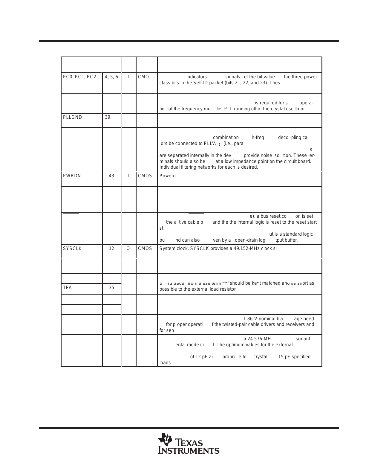
Power class indicators. the PC signals set the bit values of the three power
БББББББББББББББББ
class bits in the Self-ID packet (bits 21, 22, and 23). These bits can be programmed by tying the terminals to VCC (high) or to GND (low).
БББББББББББББББББ
PLL filter. PLLFLT is connected to a 0.1-µF capacitor and then to AGND to
complete the internal lag-lead filter. This filter is required for stable opera-
БББББББББББББББББ
tion of the frequency multiplier PLL running off of the crystal oscillator.
PLL circuit ground. The PLLGND terminals should be tied to the low-imped-
ance circuit board ground plane.
PLL circuit power. PLLVCC supplies power to the PLL portion of the device.
БББББББББББББББББ
It is recommended that a combination of high-frequency decoupling capacitors be connected to PLLVCC (i.e., paralleled 0.1 µF and 0.001 µF). Lower
БББББББББББББББББ
frequency 10-µF filtering capacitors can also be used. These supply pins
БББББББББББББББББ
are separated internally in the device to provide noise isolation. These terminals should also be tied at a low impedance point on the circuit board.
БББББББББББББББББ
Individual filtering networks for each is desired.
Powerdown. When asserted high, PWRDN turns off all internal circuitry
except the CNA monitor circuits that drive the CNA terminal.
БББББББББББББББББ
Current setting resistor. An internal reference voltage is applied to a resistor
connected between these two terminals to set the operating current and the
БББББББББББББББББ
cable driver output current. A low TCR 6 kΩ ±5% resistor should be used to
meet the IEEE 1394-1995 standard requirements for output voltage limits.
БББББББББББББББББ
Reset. When RESET is asserted low (active), a bus reset condition is set
on the active cable ports and the the internal logic is reset to the reset start
БББББББББББББББББ
state. An internal pullup resistor , which is connected to VCC, is provided so
only an external delay capacitor is required. This input is a standard logic
БББББББББББББББББ
buffer and can also be driven by an open-drain logic output buffer.
System clock. SYSCLK provides a 49.152-MHz clock signal, which is syn-
chronized with the data transfers, to the link.
БББББББББББББББББ
Test mode control. TESTM1 and TESTM2 are used during manufacturing
test and should be tied to VCC.
Port cable pair A. TPA is the port A connection to the twisted pair cable.
p
possible to the external load resistors and to the cable connector.
Port cable pair B. TPB is the port B connection to the twisted pair cable.
БББББББББББББББББ
p
possible to the external load resistors and to the cable connector.
Twisted-pair bias. TPBIAS provides the 1.86-V nominal bias voltage need-
ed for proper operation of the twisted-pair cable drivers and receivers and
БББББББББББББББББ
for sending a valid cable connection signal to the remote nodes.
Crystal oscillator. X0 and X1 connect to a 24.576-MHz parallel resonant
fundamental mode crystal. The optimum values for the external shunt ca-
БББББББББББББББББ
pacitors are dependent on the specifications of the crystal used. The sug-
БББББББББББББББББ
gested values of 12 pF are appropriate for a crystal with 15 pF specified
loads.
POST OFFICE BOX 655303 • DALLAS, TEXAS 75265
7
Page 8

TSB11LV01
C
V
High- or low-level output current, I
I
3-V 1-PORT IEEE 1394-1995 CABLE TRANSCEIVER/ARBITER
SLLS232B – MARCH 1996 – REVISED MA Y 1997
absolute maximum ratings over operating free-air temperature range (unless otherwise noted)
Supply voltage range, V
Input voltage range, V
Output voltage range at any output, V
CC
I
O
–0.5 V to VCC + 0.5 V. . . . . . . . . . . . . . . . . . . . . . . . . . . . . . . . . . . . . . . . . . . . . . . . . . . . . .
–0.5 V to VCC + 0.5 V. . . . . . . . . . . . . . . . . . . . . . . . . . . . . . . . . . . . . . .
Continuous total power dissipation See Dissipation Rating Table. . . . . . . . . . . . . . . . . . . . . . . . . . . . . . . . . . . . . .
Operating free air temperature, T
Storage temperature range, T
A
stg
Lead temperature 1,6 mm (1/16 inch) from case for 10 seconds 300°C. . . . . . . . . . . . . . . . . . . . . . . . . . . . . . . .
†
Stresses beyond those listed under “absolute maximum ratings” may cause permanent damage to the device. These are stress ratings only, and
functional operation of the device at these or any other conditions beyond those indicated under “recommended operating conditions” is not
implied. Exposure to absolute-maximum-rated conditions for extended periods may affect device reliability.
DISSIPATION RATING TABLE
PACKAGE
PT 1315 mW 10.5 mW/°C 842 mW
†
This is the inverse of the traditional junction-to-case thermal resistance (R
board-mounted 95°C/W.
TA ≤ 25°C
POWER RATING
OPERATING FACTOR
ABOVE TA = 25°C
†
TA = 70°C
POWER RATING
θJA
) and uses a
–0.5 V to 4 V. . . . . . . . . . . . . . . . . . . . . . . . . . . . . . . . . . . . . . . . . . . . . . . . . . . . . . . . . .
0°C to 70°C. . . . . . . . . . . . . . . . . . . . . . . . . . . . . . . . . . . . . . . . . . . . . . . . . . . . .
–65°C to 150°C. . . . . . . . . . . . . . . . . . . . . . . . . . . . . . . . . . . . . . . . . . . . . . . . . . . .
recommended operating conditions
MIN NOM MAX UNIT
Supply voltage, V
Supply voltage, V
High-level input voltage, V
Low-level input voltage, V
Differential input voltage, V
ommon-mode input voltage,
Receive input jitter
Receive input skew
Output current, I
‡
This parameter is for a node that does not source power (see section 4.2.2.2 in IEEE 1394-1995 standard).
CC(SP)
CC(NSP)
p
O
IH
IL
ID
IC
or
OL
CMOS inputs
CMOS inputs
Cable inputs
Cable inputs, VCC > 3 V
Cable inputs, VCC < 3 V
TPA, TPB cable inputs
Between TPA and TPB cable inputs
SYSCLK
OH
CTL0, CTL1, D0, D1, CNA
TPBIAS
0.7 V
1.165
1.165
2.7
CC
142
–16
–12
–2
3
3.3
‡
3
3.6
3.6
0.2 VCC
260
2.515
2.015
±1.08
±0.8
16
12
V
V
V
V
mV
V
‡
V
ns
ns
mA
mA
1
mA
†
electrical characteristics over recommended ranges of operating conditions (unless otherwise
noted)
driver
V
OD
I
(DIFF)
V
D
§
This parameter limits are defined as algebraic sum of TPA+ and TP A– driver currents. These limits also apply to TPB+ and TPA– algebraic sum
of driver currents.
8
Differential output voltage
Driver difference output current
Off-state voltage
PARAMETER TEST CONDITION
56-Ω load
Driver enabled
POST OFFICE BOX 655303 • DALLAS, TEXAS 75265
MIN MAX UNIT
172
–1.05
265
§
1.05
§
20
mV
mA
mV
Page 9

Á
Á
Á
Á
Á
Á
БББББББББББ
БББББББББББ
БББББББББББ
Á
БББББББББББ
Á
Á
Á
Á
БББББББББББ
БББББББББББ
БББББББББББ
Pull
RESET
БББББББББББ
БББББББББББ
Á
БББББББББББ
Á
Á
Á
Á
Á
Á
Á
Á
receiver
I
IC
z
ID
Á
z
IC
V
IT1
device
V
IT2
V
OH
V
OL
ÁÁ
I
OZ
V
(TO)+
V
(TO)–
ÁÁ
V
O
I
CC
I
CC(PD)
3-V 1-PORT IEEE 1394-1995 CABLE TRANSCEIVER/ARBITER
PARAMETER TEST CONDITION
Common-mode input current
Differential input impedance
ББББББББББББББ
Common-mode input impedance
Receiver input threshold voltage
Cable-bias detect threshold, TPB cable input
PARAMETER TEST CONDITION
Power status input threshold voltage (CPS)
High-level output voltage
Low-level output voltage
Input current
(LREQ, LPS, PD, PC0, PC1, PC2)
ББББББББББ
High-impedance-state output current
(CTL0, CTL1, D0, D1, C/LKON)
up input current,
Power-up reset time, RESET
Positive arbitration comparator threshold
voltage
Negative arbitration comparator threshold
ББББББББББ
voltage
TPBIAS output voltage
Supply current, receiver active VCC = 3.6 V
Supply current, power-down mode VCC = 3 V
400-kΩ resistor
IOH = max,
IOL = min,
VI=VCC or 0
БББББББ
VO= VCC or 0
VI =1.5 V
VI =0
SLLS232B – MARCH 1996 – REVISED MA Y 1997
Driver disabled
Driver disabled
ББББББББ
Driver disabled
Driver disabled
MIN TYP MAX UNIT
4.7
VCC = min
VCC –0.55
VCC = max
ÁÁÁÁÁÁÁÁ
–20
–22
2
89
ÁÁÁÁÁÁÁ
–168
1.665
TSB11LV01
MIN MAX UNIT
–20
5
Á
–40
–45
ÁÁÁÁ
10
Á
20
–30
0.6
2.015
20
24
30
7.5
0.5
±1
±5
–80
–90
168
–89
115
µA
kΩ
pF
6
Á
kΩ
pF
mV
1
V
V
V
V
µA
Á
µA
µA
µA
ms
mV
mV
Á
V
mA
mA
thermal characteristics
PARAMETER TEST CONDITION
R
R
Junction-to-free-air thermal resistance
θJA
Junction-to-case-thermal resistance
θJA
switching characteristics
PARAMETER
Jitter, transmit
Skew time, transmit
t
Rise time, transmit
r
t
Fall time, transmit
f
Setup time, D, CTL, LREQ low or high before
t
su
SYSCLK
Hold time, D, CTL, LREQ low or high after
t
h
SYSCLK
t
Delay time, SYSCLK high to D, CTL low or high
d
Board mounted,
MEASURED
TPA, TPB
Between TPA and TPB
10% to 90%
90% to 10%
50% to 50%
50% to 50%
БББББ
50% to 50%
No air flow
TEST CONDITION
RL = 55 Ω, CL = 10 pF
RL = 55 Ω, CL = 10 pF
See Figure 1
See Figure 1
БББББ
See Figure 2
MIN TYP MAX UNIT
Á
95
19
MIN
5
2
ÁÁÁÁ
2
MAX
±0.8
±0.4
3.2
3.2
11
°C/W
°C/W
UNIT
ns
ns
ns
ns
ns
ns
ns
POST OFFICE BOX 655303 • DALLAS, TEXAS 75265
9
Page 10

TSB11LV01
3-V 1-PORT IEEE 1394-1995 CABLE TRANSCEIVER/ARBITER
SLLS232B – MARCH 1996 – REVISED MA Y 1997
PARAMETER MEASUREMENT INFORMATION
SYSCLK
D, CTL, LREQ
t
su
50%
t
h
50%50%
Figure 1. D, CTL, LREQ Input Setup and Hold Timing Waveforms
SYSCLK
D, CTL
50%
t
d
50%
Figure 2. D and CTL Output Delay Timing Waveforms
APPLICATION INFORMATION
TSB11LV01
Cable Port
TPBIAS
TPA+
TPA–
TPB+
TPB–
25
56 Ω
36
35
34
33
56 Ω
250 pF
1 µF TYP
56 Ω
56 Ω
5 kΩ
Figure 3. Twisted-Pair Cable Interface Connections
Cable
Pair
A
Cable
Pair
B
10
POST OFFICE BOX 655303 • DALLAS, TEXAS 75265
Page 11

Á
Á
Á
Á
Á
Á
Á
Á
Á
Á
Á
Á
Á
Á
Á
Á
Á
Á
Á
Á
Á
Á
Á
Á
Á
Á
Á
Á
Á
Á
Á
Á
Á
Á
Á
Á
Á
Á
Á
Á
TSB11LV01
3-V 1-PORT IEEE 1394-1995 CABLE TRANSCEIVER/ARBITER
SLLS232B – MARCH 1996 – REVISED MA Y 1997
APPLICATION INFORMATION
internal register configuration
The accessible internal registers of this device are listed in Table 1. Descriptions of the internal register fields
are given in Table 2.
Table 1. Accessible Internal Registers
Address 0 1 2 3 4 5 6 7
0000 Physical ID R CPS
0001 RHB IBR GC
0010 SPD Rev NP
0011 AStat BStat Ch Con Reserved
0100 Reserved
0101 Reserved
0110 Looplnt CPSlnt CPS IR Reserved
0111 Reserved
1000 Reserved
Field
ÁÁ
ÁÁ
AStat
ÁÁ
ÁÁ
ÁÁ
ÁÁ
BStat
ÁÁ
ÁÁ
Ch
ÁÁ
ÁÁ
Con
ÁÁ
ÁÁ
CPS
ÁÁ
Size
(Bits)
Á
Á
2
Á
Á
Á
Á
2
Á
Á
1
Á
Á
1
Á
Á
1
Á
Type
ÁÁÁ
ÁÁÁ
Read only
ÁÁÁ
ÁÁÁ
ÁÁÁ
ÁÁÁ
Read only
ÁÁÁ
ÁÁÁ
Read only
ÁÁÁ
ÁÁÁ
Read only
ÁÁÁ
ÁÁÁ
Read only
ÁÁÁ
CPSInt 1 Read/Write
Table 2. Internal Register Field Descriptions
ББББББББББББББББББББББ
AStat contains the line state of TPA. The status is indicated by the following:
11 = Z
01 = 1
10 = 0
00 = Invalid data state. Power-up reset initializes to this line state. This line state is also output during transmit and receive operations. The line state outputs are generally valid during arbitration and
idle conditions on the bus.
BStat contains the line state of TPB. The status is indicated by the following:
11 = Z
01 = 1
10 = 0
00 = Invalid data state. Power up reset initializes to this line state. This line state is also output during transmit and receive operations. The line state outputs are generally valid during arbitration and
idle conditions on the bus.
When Ch = 1, the port is a child, otherwise it is a parent. This bit is invalid after a hardware reset or a
bus reset until tree-ID processing is completed.
Con indicates the connection status of the port. When Con = 1, the port is connected, otherwise it is
disconnected. This bit is set to 1 by a hardware reset and is updated to reflect the actual cable connection status of the port during bus reset. The TSB11LV01 contains connection debounce circuitry
that prevents a new cable connection on a port from initiating a bus reset until the connection status
has been stable for at least 335 ms. Similarly, a cable disconnect must be stable for 1.3 ms before a
bus reset is initiated.
Cable power status (CPS) contains the status of the CPS input terminal. When cable power voltage
has dropped too low for reliable operation, this bit is reset (0). This bit is included twice in the internal
registers to expedite handling of the CPSInt.
CPSint indicates that a cable power status interrupt has occurred. This interrupt occurs whenever the
CPS input goes low. The interrupt indicates that the cable power voltage has dropped too low to ensure
reliable operation. This bit is cleared (0) by a hardware reset or by writing a 0 to this register. However,
if the CPS input is still low, another cable power status interrupt immediately occurs.
Description
POST OFFICE BOX 655303 • DALLAS, TEXAS 75265
11
Page 12

TSB11LV01
Á
Á
Á
Á
Á
Á
Á
Á
Á
Á
Á
Á
Á
Á
Á
Á
Á
Á
Á
Á
Á
Á
Á
Á
Á
Á
Á
Á
Á
Á
Á
Á
Á
Á
Á
Á
Á
Á
Á
Á
3-V 1-PORT IEEE 1394-1995 CABLE TRANSCEIVER/ARBITER
SLLS232B – MARCH 1996 – REVISED MA Y 1997
Table 2. Internal Register Field Descriptions (continued)
Field
ÁÁÁ
ÁÁÁ
ÁÁÁ
GC
ÁÁÁ
ÁÁÁ
IBR 1 Read/Write
IR
ÁÁÁ
ÁÁÁ
LoopInt
ÁÁÁ
ÁÁÁ
NP
Physical ID
ÁÁÁ
R
ÁÁÁ
Rev
RHB
ÁÁÁ
SPD
ÁÁÁ
Size
Á
(Bits)
Á
Á
6
Á
Á
1
Á
Á
1
Á
Á
4
6
Á
1
Á
2
1
Á
2
Á
Type
ÁÁ
ÁÁ
ÁÁ
Read/Write
ÁÁ
ÁÁ
Read/Write
ÁÁ
ÁÁ
Read/Write
ÁÁ
ÁÁ
Read only
Read only
ÁÁ
Read only
ÁÁ
Read only
Read/Write
ÁÁ
Read only
ÁÁ
БББББББББББББББББББББББ
Description
The gap count (GC) register sets the fair and arb-reset gap times. The gap count may be set to a
particular value to optimize bus performance. Typically, the gap count should be set to 2 times the
maximum number of hops on the bus and should be set to the same value for all nodes on the bus.
The gap count can be set by either a write to this register or by reception or transmission of a
PHY_CONFIG packet. The gap count is reset to a 3Fh after a hardware reset or after two consecutive bus resets without an intervening write to the gap count register (either a write to the gap count
register by the link or a PHY_CONFIG packet).
When set, initiate bus reset (IBR) causes this node to immediately initiate a bus reset. IBR is cleared
(0) after a hardware reset or a bus reset.
IR indicates that the last bus reset was initiated in this TSB11LV01 phy. This bit is also included in
the Self-ID packet.
LoopInt indicates that a configuration loop timeout has occurred. This interrupt occurs when the arbitration controller waits for too long a period of time during tree-ID. This interrupt can indicate that
the bus is configured in a loop. This bit is cleared (0) by a hardware reset or by writing a 0 to this
register bit. It should be noted that the TSB11LV01 never generates this interrupt since it has only
one available port and, therefore, cannot be part of a loop.
The number of ports (NP) contains the number of ports implemented in the core logic (not the number of ports actually on the device). For the TSB11LV01, NP is set to 0011.
Physical ID contains the physical address of the local node. The physical ID defaults to a 09h after a
hardware reset or a bus reset until the Self-ID process has been completed. A complete Self-ID is
indicated by an unsolicited status transfer of the register 0 contents to the link.
R indicates whether this node is the root node or not. This bit is cleared (0) on a hardware reset or a
bus reset. This bit is set during tree-ID when this node is root.
The revision (Rev) bits indicate the design revision of the core logic. For the TSB11LV01, Rev is set
to 01.
When set, the root hold-off bit (RHB) instructs the local node to try to become the root during the
next bus reset. RHB is reset (0) during a hardware reset and is not affected by a bus reset.
The speed (SPD) bits indicates the top signaling speed of the local port and for the TSB11LV01 is
set to 00.
12
POST OFFICE BOX 655303 • DALLAS, TEXAS 75265
Page 13

TSB11LV01
3-V 1-PORT IEEE 1394-1995 CABLE TRANSCEIVER/ARBITER
SLLS232B – MARCH 1996 – REVISED MA Y 1997
APPLICATION INFORMATION
CNAOUT
LINKV
DD
BUS MANAGER
LKON
POWER-CLASS
PROGRAMMING
LINK LAYER
CONTROLLER
INTERFACE
10 kΩ
1
2
3
4
5
6
7
8
9
10
11
12
0.1 µF
CC
V
48 47 46 45 44 43 42 41 40 39 38 37
TESTM1
CNA
LPS
C/LKON
PC0
PC1
PC2
LREQ
CTL0
CTL1
D0
D1
SYSCLK
TESTM2
CC
DV
DGND
13 14 15 16 17 18 19 20 21 22 23 24
CC
V
CCAVCC
DV
RESET
TSB11LV01
DGND
BIAS–5 V
DGND
0.1 µF
CC
POWER DOWN
PWRDN
CC
DV
V
PLLFLT
DGND
CC
PLLV
DGND
PLLGND
PLLGND
AVCCAGND
AGND
12 pF
XI
12 pF
24.576 MHz
XO
TPA+
TPA–
TPB+
TPB–
R0
R1
CPS
AV
CC
AV
CC
AGND
AGND
TPBIAS
AGND
36
35
34
33
32
31
30
29
28
27
26
25
6 kΩ
400 kΩ
1 µF
TP CABLES
CABLE POWER
V
CC
TPBIAS
V
CC
CC
LINKV
V
CC
V
CC
Figure 4. External Component Connections
POST OFFICE BOX 655303 • DALLAS, TEXAS 75265
13
Page 14

TSB11LV01
Á
Á
Á
БББББ
БББББ
БББББ
3-V 1-PORT IEEE 1394-1995 CABLE TRANSCEIVER/ARBITER
SLLS232B – MARCH 1996 – REVISED MA Y 1997
PRINCIPLES OF OPERATION
The TSB1 1L V01 is designed to operate with a link layer controller such as the Texas Instruments TSB12C01A.
These devices use a direct-connect interface such as described in Annex J of the IEEE 1394-1995 standard.
Details of how the TSB12C01A (link) devices operates are described in the TSB12C01A data sheet. The
following paragraphs describes the operation of the phy-link interface.
The TSB1 1LV01 supports 100 Mbits/s data transfers, and has two bidirectional data lines (D0 and D1) crossing
the interface. In addition there are two bidirectional control lines (CTL0 and CTL1), the 50-MHz SYSCLK line
from the phy to the link, and the link request line (LREQ) from the link to the phy . The TSB11L V01 phy has control
of all the bidirectional terminals. The link is allowed to drive these terminals only after it has been given
permission by the phy . The dedicated LREQ request terminal is used by the link for any activity that it wishes
to initiate.
There are four operations that may occur in the phy-link interface: request, status, transmit, and receive. With
the exception of the request operation, all actions are initiated by the phy.
When the phy has control of the bus, the CTL0 and CTL1 lines are encoded as shown in Table 3.
Table 3. CTL Status When Phy Has Control of the Bus
CTL0, CTL1
00
01
10
11
Name
Idle
Status
Receive
Transmit
Description of Activity
No activity is occurring (this is the default mode)
Status information is being sent from the phy to the link
An incoming packet is being sent from the phy to the link
The link has been given control of the bus to send an outgoing packet
When the link has control of the bus (with phy permission), the CTL0 and CTL1 lines are encoded as shown
in Table 4.
Table 4. CTL Status When Link Has Control of the Bus
CTL0, CTL1
00
01
ÁÁÁ
10
11
Name
Idle
Hold
ÁÁ
Transmit
Reserved
Description of Activity
The link releases the bus (transmission has been completed)
The link is holding the bus while data is being prepared for transmission or sending another
БББББББББББББББББББББ
packet without arbitrating
An outgoing packet is being sent from the link to the phy
None
When the link wishes to request the bus or access a register that is located in the TSB1 1LV01 phy , a serial stream
of information is sent across the LREQ line. The length of the stream varies depending on whether the transfer
is a bus request, a read command, or a write command (see T able 5). Regardless of the type of transfer, a start
bit of 1 is required at the beginning of the stream, and a stop bit of 0 is required at the end of the stream. Bit 0
is the most significant, and is transmitted first. The LREQ terminal is required to idle low.
Table 5. Link Bus Request or Register Access Request Bit Length
14
Request Type
Bus Request
Read Register Request
Write Register Request
POST OFFICE BOX 655303 • DALLAS, TEXAS 75265
Number of Bits
7
9
17
Page 15

3-V 1-PORT IEEE 1394-1995 CABLE TRANSCEIVER/ARBITER
SLLS232B – MARCH 1996 – REVISED MA Y 1997
PRINCIPLES OF OPERATION
For a Bus Request the length of the LREQ data stream is 7 bits and is shown in Table 6.
Table 6. Link Bus Request
TSB11LV01
Bit(s)
0
1–3
4–5
6
Name
Start Bit
Request Type
Request Speed
Stop Bit
Description
This bit indicates the beginning of the transfer (always 1).
These bits indicate the type of bus request (see Table 9 for the encoding of this field).
These bits should always be 00 for TSB11LV01 100 Mbits/s speed.
This bit indicates the end of the transfer (always 0).
For a Read Register Request the length of the LREQ data stream is 9 bits and is shown in Table 7.
Table 7. Link Read Register Access
Bit(s)
0
1–3
4–7
8
Name
Start Bit
Request Type
Address
Stop Bit
Description
This bit indicates the beginning of the transfer (always 1).
These bits are always 100 indicating that this is a read register request.
These bits are the address of the phy register to be read.
This bit indicates the end of the transfer (always 0).
For a Write Register Request the length of the LREQ data stream is 17 bits and is shown in Table 8.
Table 8. Link Write Register Access
Bit(s)
0
1–3
4–7
8–15
16
Name
Start Bit
Request Type
Address
Data
Stop Bit
Description
This bit indicates the beginning of the transfer (always 1).
These bits are always 101 indicating that this is a write register request.
These bits are the address of the phy register to be written to.
These bits are the data that is written to the specified register address.
This bit indicates the end of the transfer (always 0).
The 3-bit Request Type fields are described in Table 9.
Table 9. Link Bus Request Type
LREQ1 – LREQ3
000
001
010
011
100
101
110, 111
Name
ImmReq
IsoReq
PriReq
FairReq
RdReg
WrReg
Reserved
Immediate request. When an idle is detected, take control of the bus immediately (no arbitration).
Isochronous request. Arbitrate for the bus with no gaps.
Priority request. Arbitrate after a subaction gap and ignore fair protocol.
Fair request. Arbitrate after a subaction gap and use fair protocol.
Read register. Return the specified register contents through a status transfer
Write register . W rite to the specified register.
Reserved
Description
POST OFFICE BOX 655303 • DALLAS, TEXAS 75265
15
Page 16

TSB11LV01
3-V 1-PORT IEEE 1394-1995 CABLE TRANSCEIVER/ARBITER
SLLS232B – MARCH 1996 – REVISED MA Y 1997
PRINCIPLES OF OPERATION
request
LR0 LR1 LR2 LR3 LR(n-2) LR(n-1)
NOTE A: Each cell in this timing diagram represents one clock sample time.
Figure 5. LREQ Timing
bus request
For fair or priority access, the link requests control of the bus at least one clock after the phy-link interface
becomes idle. If the link senses that the CTL terminals are in a receive state (CTL0 and CTL1 = 10), then it knows
that its request has been lost. This is true anytime during or after the link sends the bus request transfer on
LREQ. Additionally, the phy ignores any fair or priority requests if it asserts the receive state while the link is
requesting the bus. The link then reissues the request one clock after the next interface idle.
The cycle master uses a priority request to send a cycle start message. After receiving a cycle start, the link
can issue an isochronous bus request. When arbitration is won, the link proceeds with the isochronous transfer
of data. The phy clears an isochronous request only when the bus has been won. The isochronous request
register is cleared in the phy once the link sends another type of request or when the isochronous transfer has
been completed. The isochronous request must be issued during a packet reception. Usually this occurs during
the reception of a cycle start packet.
The ImmReq request is issued when the link needs to send an acknowledgment after reception of a packet
addressed to it. This request must be issued during packet reception. This is done to minimize the delays that
a phy would have to wait between the end of a packet and the transmittal of an acknowledgment. As soon as
the packet ends, the phy immediately grants access of the bus to the link. The link sends an acknowledgment
to the sender unless the header cyclic redundancy check (CRC) of the packet turns out to be bad. In this case,
the link releases the bus immediately; it is not allowed to send another type of packet on this grant. To ensure
another packet is not sent, the link is forced to wait 160 ns after the end of the packet is received. The phy then
gains control of the bus and the acknowledgment with the CRC error is sent. Then the bus is released and
allowed to proceed with another request.
Although highly improbable, it is conceivable that two separate nodes could believe that an incoming packet
is intended for them. The nodes then issue a ImmReq request before checking the CRC of the packet. Since
each phy seizes control of the bus at the same time, a temporary, localized collision of the bus occurs
somewhere between the competing nodes. This collision would be interpreted by the other nodes on the
network as being a ZZ line state and not a bus reset. As soon as the two nodes check the CRC, the mistaken
node drops its request and the false line state is removed. The only side effect would be the loss of the intended
acknowledgment packet (this is handled by the higher-layer protocol).
phy register read/write requests
When the link requests to read the specified register contents, the phy sends the contents of the register to the
link through a status transfer. If an incoming packet is received while the phy is transferring status information
to the link, the phy continues to attempt to transfer the contents of the register until it is successful.
For write requests, the phy loads the data field into the appropriately addressed register as soon as the transfer
has been completed. The link is allowed to request register read or write operations at any time.
16
POST OFFICE BOX 655303 • DALLAS, TEXAS 75265
Page 17

Á
Á
Á
Á
Á
Á
Á
Á
Á
Á
Á
Á
TSB11LV01
3-V 1-PORT IEEE 1394-1995 CABLE TRANSCEIVER/ARBITER
SLLS232B – MARCH 1996 – REVISED MA Y 1997
PRINCIPLES OF OPERATION
status
A status transfer is initiated by the phy when it has status information to transfer to the link. The phy waits until
the interface is idle before starting the transfer. The transfer is initiated by asserting the following on the the
control terminals: CTL0 and CTL1 = 01 along with the first two bits of status information on the D0 and D1
terminals. The phy maintains CTL0 and CTL1 = 01 for the duration of status transfer. The phy may prematurely
end a status transfer by asserting something else other than CTL0 and CTL1 = 01 on the control terminals. This
could be caused by an incoming packet from another node. The phy continues to attempt to complete the
transfer until the information has been successfully transmitted. There must be at least one idle cycle in between
consecutive status transfers.
The phy normally sends just the first four bits of status to the link. These bits are status flags that are needed
by the link state machines. The phy sends an entire status packet to the link after a request transfer that contains
a read request, or when the phy has pertinent information to send to the link or transaction layers. The only
defined condition where the phy automatically sends a register to the link is after Self-ID, when it sends the
Physical-ID register , which contains the new node address.
The descriptions of the bits in the status transfer are listed in Table 10 and the timing is shown in Figure 6.
Bit(s)
0
ÁÁÁÁ
ÁÁÁÁ
1
ÁÁÁÁ
2
3
ÁÁÁÁ
4–7
8–15
CTL0, CTL1
Name
Arbitration Reset Gap
БББББ
БББББ
Subaction Gap
БББББ
Bus Reset
CPS
БББББ
Address
Data
Phy
Phy
D0, D1
Table 10. Status Transfer Bit Description
Description
This bit indicates that the phy has detected that the bus has been idle for an arbitration
reset gap time (this time is defined in the IEEE 1394-1995 standard). This bit is used by
ББББББББББББББББББББ
the link in its busy/retry state machine.
This bit indicates that the phy has detected that the bus has been idle for a subaction gap
ББББББББББББББББББББ
time (this time is defined in the IEEE 1394-1995 standard). This bit is used by the link to
detect the completion of an isochronous cycle.
ББББББББББББББББББББ
This bit indicates that the phy has entered the bus reset state.
This bit indicates that the cable power has dropped below the threshold for reliable op-
ББББББББББББББББББББ
eration.
These bits hold the address of the phy register whose contents are transferred to the link.
These bits contain the data that is to be sent to the link.
00 01 01 01 00 00
00 S[0,1] 00 00
S[2,3] S[14,15]
Figure 6. Status Transfer Timing
POST OFFICE BOX 655303 • DALLAS, TEXAS 75265
17
Page 18

TSB11LV01
3-V 1-PORT IEEE 1394-1995 CABLE TRANSCEIVER/ARBITER
SLLS232B – MARCH 1996 – REVISED MA Y 1997
PRINCIPLES OF OPERATION
transmit
When the link wants to transmit information, it first requests access to the bus through the LREQ terminal. Once
the phy receives this request, it arbitrates to gain control of the bus. When the phy wins ownership of the serial
bus, it grants the bus to the link by asserting the transmit state on the CTL terminals for at least one SYSCLK
cycle. The link takes control of the bus by asserting either hold or transmit on the CTL lines. Hold is used by
the link to keep control of the bus when it needs some time to prepare the data for transmission. The phy keeps
control of the bus for the link by asserting a data-on state on the bus. It is not necessary for the link to use hold
when it is ready to transmit as soon as bus ownership is granted.
When the link is prepared to send data, it asserts transmit on the CTL lines as well as sending the first bits of
the packet on the D0 and D1 lines (assuming 100 Mbits/s). The transmit state is held on the CTL terminals until
the last bits of data have been sent. The link then asserts idle on the CTL lines for one clock cycle after which
it releases control of the interface.
However, there are times when the link needs to send another packet without releasing the bus. For example,
the link may want to send consecutive isochronous packets or it may want to attach a response to an
acknowledgment. To do this, the link asserts a hold instead of an idle when the first packet of data has been
completely transmitted. Hold, in this case, informs the phy that the link needs to send another packet without
releasing control of the bus. The phy then waits a set amount of time before asserting transmit. The link can
then proceed with the transmittal of the second packet. After all data has been transmitted and the link has
asserted idle on the CTL terminals, the phy asserts its own idle state on the CTL lines. When sending multiple
packets in this fashion, it is required that all data be transmitted at the same speed. This is required because
the transmission speed is set during arbitration and since the arbitration step is skipped, there is no way of
informing the network of a change in speed.
Single Packet
Phy
CTL0, CTL1
Phy
D0, D1
Link
CTL0, CTL1
Link
D0, D1
Continued Packet
Phy
CTL0, CTL1
Phy
D0, D1
Link
CTL0, CTL1
Link
D0, D1
NOTE A: ZZ = High Impedance State
D0 => Dn = Packet data
11 00 ZZ ZZ ZZ ZZ
00 00 ZZ ZZ ZZ ZZ
ZZ ZZ 01 10 10 10
ZZ ZZ 00 D0 D1 D2
ZZ
ZZ ZZ 00 11 00 ZZ
ZZ ZZ 00 00 00 ZZ
01 00 ZZ ZZ ZZ 01
00 00 ZZ ZZ ZZ 00
Figure 7. Transmit Timing Waveforms
ZZ ZZ 00ZZ ZZ00
ZZ ZZ 00ZZ ZZ00
00 00 ZZ01 10ZZ
00 00 ZZ00 DnZZ
ZZ ZZ ZZ00ZZ
ZZ ZZ ZZ00ZZZZ
01 10 10ZZ1010
00 D0 D1ZZDnDn-1
18
POST OFFICE BOX 655303 • DALLAS, TEXAS 75265
Page 19

Á
Á
TSB11LV01
3-V 1-PORT IEEE 1394-1995 CABLE TRANSCEIVER/ARBITER
SLLS232B – MARCH 1996 – REVISED MA Y 1997
PRINCIPLES OF OPERATION
receive
When data is received by the phy from the serial bus, the phy transfers the data to the link for further processing.
The phy asserts receive on the CTL lines and asserts each D terminal high. The phy indicates the start of the
packet by placing the speed code on the data bus. The phy then proceeds with the transmittal of the packet to
the link on the D lines while still keeping the receive status on the CTL terminals. Once the packet has been
completely transferred, the phy asserts idle on the CTL terminals, which completes the receive operation.
NOTE
The speed is a phy-link protocol and not included in the CRC.
Phy
CTL0, CTL1
Phy
D0, D1
NOTE A: SPD = Speed Code
D0 => Dn = Packet data
10 10 10 10
11 SPD D0 D1
10 00 001000
Dn 00 001100
Figure 8. Receive Timing Waveforms
Table 11. Speed Code For the Receiver
Speed Code
ÁÁÁÁ
(D0, D1)
00
Data Rate
ÁÁÁÁ
100 Mbits/s
power class bits in the Self-ID packet
Table 12 contains a description of each power class bit in the power field (bits 21, 22, and 23) of the Self-ID
packet.
Table 12. Self-ID Packet Power Field Bit Description
PC0 – PC2 Description
000 Node does not need power and does not repeat power.
001 Node is self powered and provides a minimum of 15 W to the bus.
010 Node is self powered and provides a minimum of 30 W to the bus.
011 Node is self powered and provides a minimum of 45 W to the bus.
100 Node may be powered from the bus and is using up to 1 W.
101 Node may be powered from the bus and is using up to 1 W. An additional 2 W is needed to enable the link and higher layers.
110 Node may be powered from the bus and is using up to 1 W. An additional 5 W is needed to enable the link and higher layers.
111 Node may be powered from the bus and is using up to 1 W. An additional 9 W is needed to enable the link and higher layers.
POST OFFICE BOX 655303 • DALLAS, TEXAS 75265
19
Page 20

TSB11LV01
3-V 1-PORT IEEE 1394-1995 CABLE TRANSCEIVER/ARBITER
SLLS232B – MARCH 1996 – REVISED MA Y 1997
MECHANICAL INFORMATION
PT (S-PQFP-G48) PLASTIC QUAD FLATPACK
37
48
0,50
1,45
1,35
36
0,27
0,17
25
24
13
1
5,50 TYP
7,20
SQ
6,80
9,20
SQ
8,80
12
0,08
M
0,05 MIN
0,13 NOM
Gage Plane
0,25
0°–7°
1,60 MAX
NOTES: A. All linear dimensions are in millimeters.
B. This drawing is subject to change without notice.
C. Falls within JEDEC MS-026
D. This may also be a thermally enhanced plastic package with leads conected to the die pads.
Seating Plane
0,10
0,75
0,45
4040052/C 11/96
20
POST OFFICE BOX 655303 • DALLAS, TEXAS 75265
Page 21

IMPORTANT NOTICE
T exas Instruments (TI) reserves the right to make changes to its products or to discontinue any semiconductor
product or service without notice, and advises its customers to obtain the latest version of relevant information
to verify, before placing orders, that the information being relied on is current and complete.
TI warrants performance of its semiconductor products and related software to the specifications applicable at
the time of sale in accordance with TI’s standard warranty. Testing and other quality control techniques are
utilized to the extent TI deems necessary to support this warranty. Specific testing of all parameters of each
device is not necessarily performed, except those mandated by government requirements.
Certain applications using semiconductor products may involve potential risks of death, personal injury, or
severe property or environmental damage (“Critical Applications”).
TI SEMICONDUCTOR PRODUCTS ARE NOT DESIGNED, INTENDED, AUTHORIZED, OR WARRANTED
TO BE SUITABLE FOR USE IN LIFE-SUPPORT APPLICATIONS, DEVICES OR SYSTEMS OR OTHER
CRITICAL APPLICATIONS.
Inclusion of TI products in such applications is understood to be fully at the risk of the customer. Use of TI
products in such applications requires the written approval of an appropriate TI officer . Questions concerning
potential risk applications should be directed to TI through a local SC sales office.
In order to minimize risks associated with the customer’s applications, adequate design and operating
safeguards should be provided by the customer to minimize inherent or procedural hazards.
TI assumes no liability for applications assistance, customer product design, software performance, or
infringement of patents or services described herein. Nor does TI warrant or represent that any license, either
express or implied, is granted under any patent right, copyright, mask work right, or other intellectual property
right of TI covering or relating to any combination, machine, or process in which such semiconductor products
or services might be or are used.
Copyright 1998, Texas Instruments Incorporated
 Loading...