

Page 1
INTEGRATED CIRCUITS
DATA SH EET
TSA5526; TSA5527
1.3 GHz universal bus-controlled
TV synthesizers
Product specification
Supersedes data of 1995 Mar 22
File under Integrated Circuits, IC02
1996 Sep 24
Page 2
Philips Semiconductors Product specification
1.3 GHz universal bus-controlled
TV synthesizers
FEATURES
• Complete 1.3 GHz single chip system
• Four PNP band switch buffers (40 mA)
• 33 V output tuning voltage
• In-lock detector
• 5-step ADC
• 15-bit programmable divider
• Programmable reference divider ratio
(512, 640 or 1024)
• Programmable charge-pump current (60 or 280 µA)
• Programmable automatic charge-pump current switch
• Varicap drive disable
2
• Universal bus protocol I
– bus protocol for 18 or 19 bits transmission
(3-wire bus)
– extra protocol for 27 bits for test and features
(3-wire bus)
– address plus 4 data bytes transmission (I2C-bus write
mode)
– address plus 1 status byte transmission (I2C-bus
read mode)
– three independent I2C-bus addresses
• Low power and low radiation.
C-bus or 3-wire bus:
TSA5526; TSA5527
APPLICATIONS
• TV tuners and front ends
• VCR tuners.
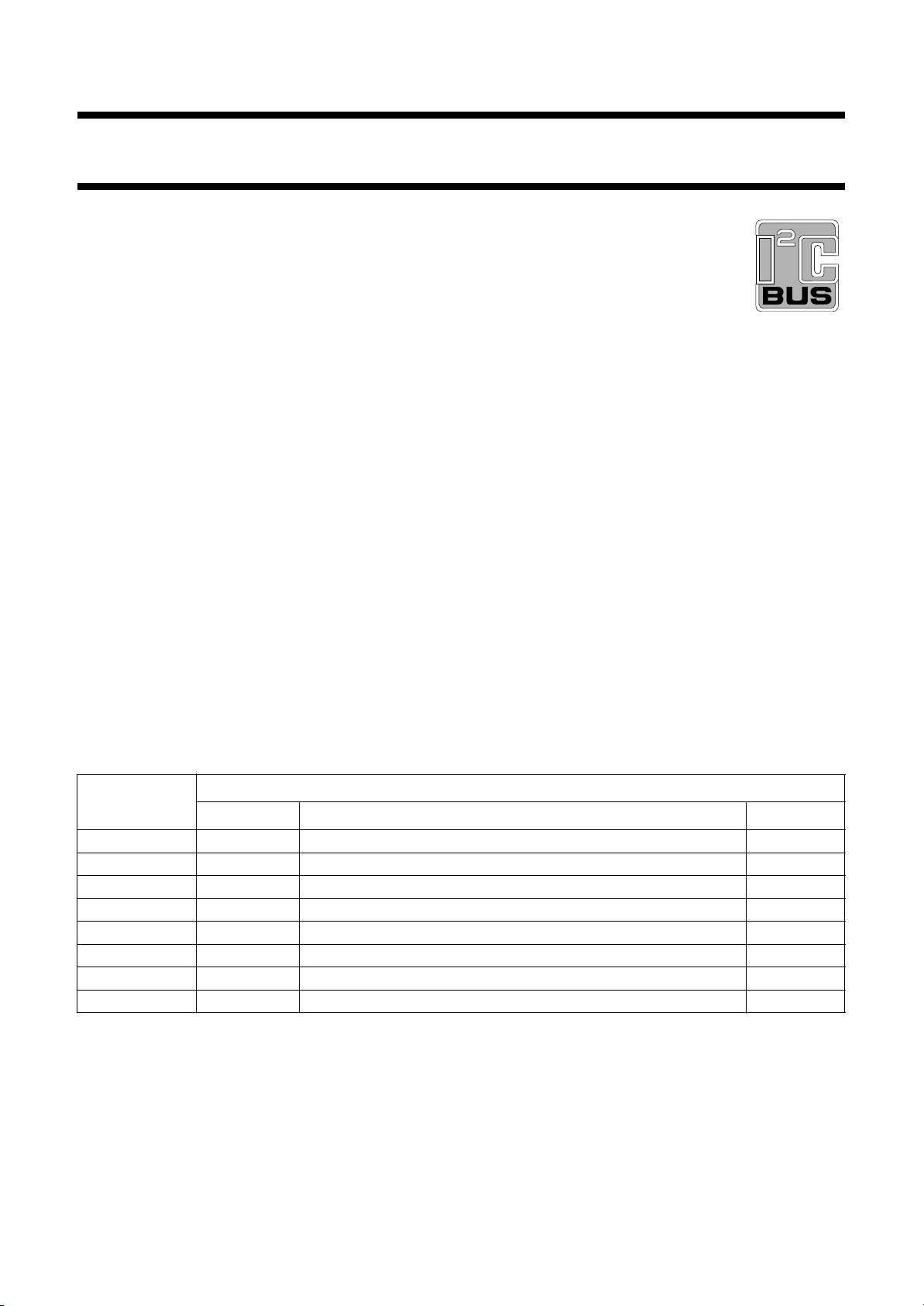
ORDERING INFORMATION
TYPE NUMBER
NAME DESCRIPTION VERSION
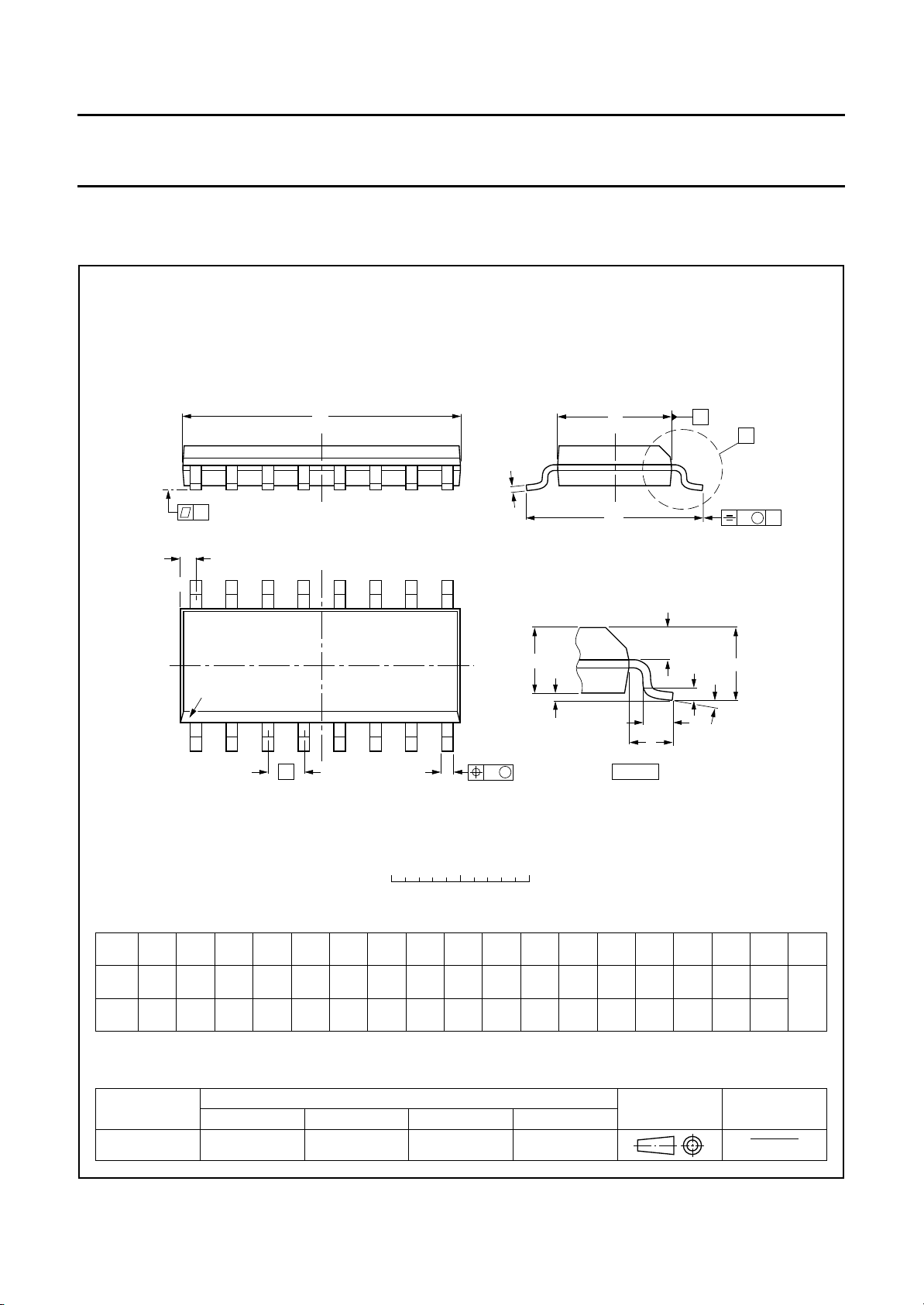
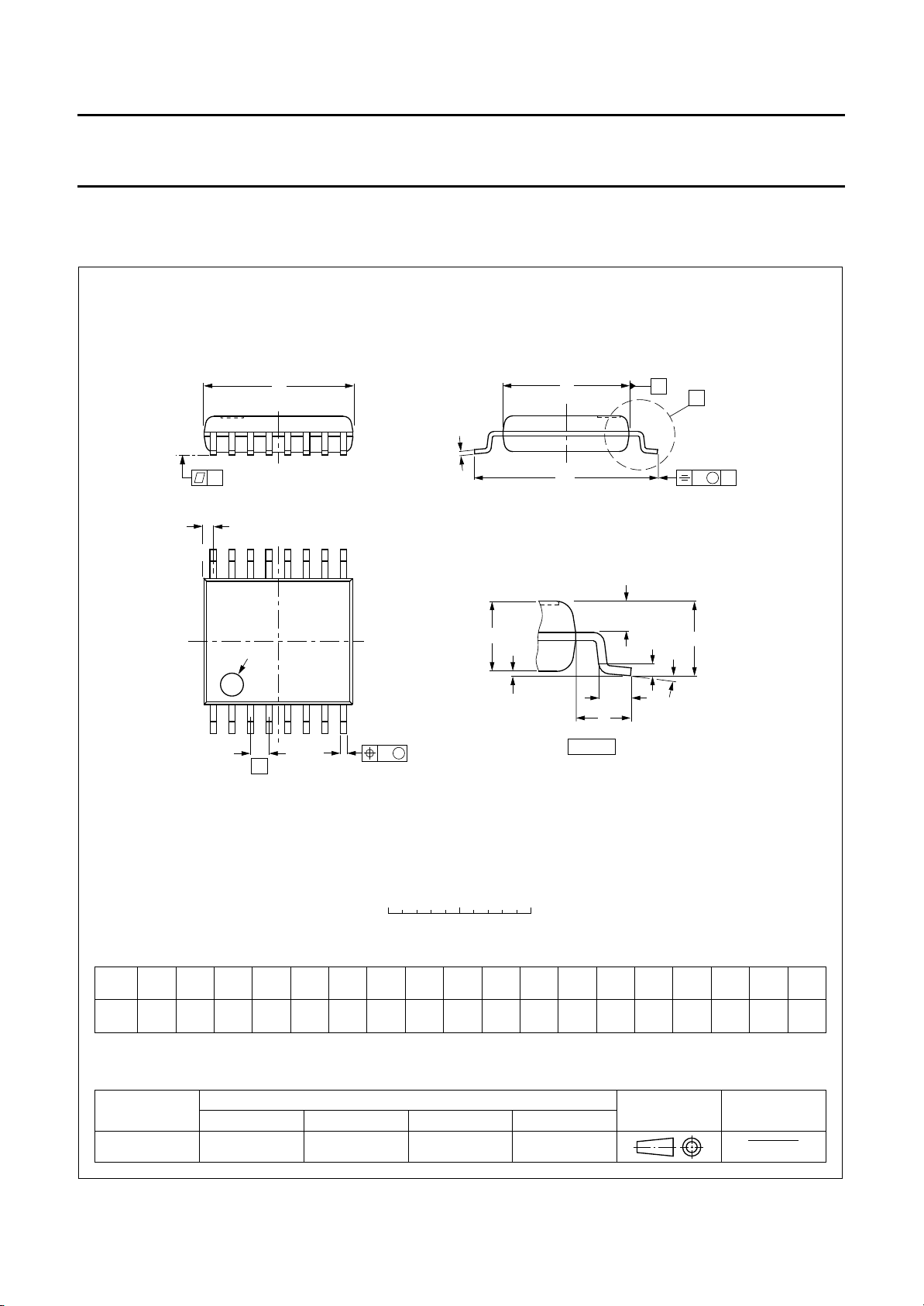
TSA5526M SSOP16 plastic shrink small outline package; 16 leads; body width 4.4 mm SOT369-1
TSA5526T SO16 plastic small outline package; 16 leads; body width 3.9 mm SOT109-1
TSA5527M SSOP16 plastic shrink small outline package; 16 leads; body width 4.4 mm SOT369-1
TSA5527T SO16 plastic small outline package; 16 leads; body width 3.9 mm SOT109-1
TSA5526AM SSOP16 plastic shrink small outline package; 16 leads; body width 4.4 mm SOT369-1
TSA5526AT SO16 plastic small outline package; 16 leads; body width 3.9 mm SOT109-1
TSA5527AM SSOP16 plastic shrink small outline package; 16 leads; body width 4.4 mm SOT369-1
TSA5527AT SO16 plastic small outline package; 16 leads; body width 3.9 mm SOT109-1
1996 Sep 24 2
PACKAGE
Page 3
Philips Semiconductors Product specification
1.3 GHz universal bus-controlled
TSA5526; TSA5527
TV synthesizers
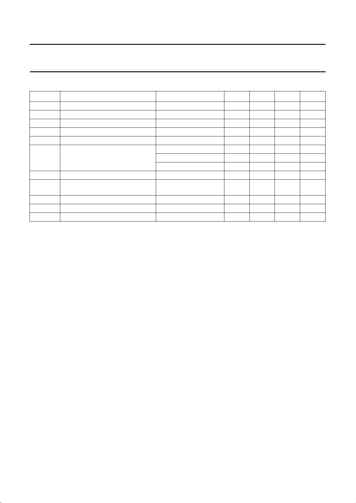
QUICK REFERENCE DATA
SYMBOL PARAMETER CONDITIONS MIN. TYP. MAX. UNIT
V
CC1
V
CC2
I
CC1
I
CC2
f
RF
V
i(RF)
f
xtal
I
o(PNP)
P
tot
T
stg
T
amb
supply voltage (+5 V) 4.5 − 5.5 V
band switch supply voltage (12 V) V
CC1
12 13.5 V
supply current − 20 25 mA
band switch supply current note 1 − 50 55 mA
RF input frequency 64 − 1300 MHz
RF input voltage fi= 80 to 150 MHz −25 − 3 dBm
= 150 to 1000 MHz −28 − 3 dBm
f
i
f
= 1000 to 1300 MHz −15 − 3 dBm
i
crystal oscillator input frequency 3.2 4.0 4.48 MHz
PNP band switch buffers output
note 2 4 − 50 mA
current
total power dissipation note 3 − 250 400 mW
storage temperature −40 − +150 °C
operating ambient temperature −20 − +85 °C
Notes
1. One band switch buffer ON, I
= 40 mA.
o
2. One band switch buffer ON, Io= 40 mA; two buffers ON, maximum sum of Io=50mA.
3. The power dissipation is calculated as follows:
P
V
D
CC1ICC1VCC2ICC2Io
–()I
V
o
CE satPNP()
V33 2⁄()
2
27⁄+×+×+×=
kΩ.
1996 Sep 24 3
Page 4
Philips Semiconductors Product specification
1.3 GHz universal bus-controlled
TV synthesizers
GENERAL DESCRIPTION
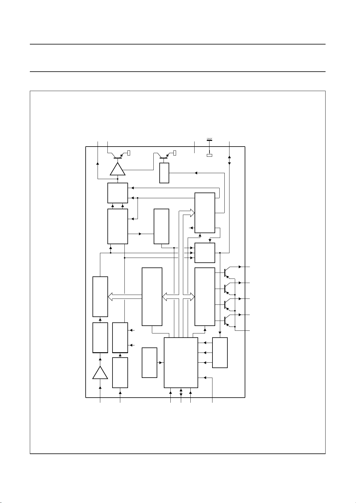
The device is a single-chip PLL frequency synthesizer
designed for TV and VCR tuning systems. The circuit
consists of a divide-by-eight prescaler with its own
preamplifier, a 15-bit programmable divider, a crystal
oscillator and its programmable reference divider and a
phase/frequency detector combined with a charge-pump
which drives the tuning amplifier and the 33 V output.
Four high-current PNP band switch buffers are provided
for band switching. Two PNP buffers can be switched on
simultaneously. The sum of the collector currents is limited
to 50 mA.
Depending on the reference divider ratio (512, 640 or
1024), the phase comparator operates at 3.90625 kHz,
6.25 kHz or 7.8125 kHz using a 4 MHz crystal.
The device can be controlled in accordance with the
2
C-bus format or the 3-wire bus format depending on the
I
voltage applied to the SW input (see Table 2). In the 3-wire
bus mode (SW = HIGH) pin 12 is the LOCK output.
The lock output is LOW when the PLL loop is locked. In the
I2C-bus mode (SW = LOW) the LOCK detector bit FL is set
to logic 1 when the loop is locked and is read on the SDA
line (status byte) during a read operation. The ADC input
is available on pin 12 for AFC control in the I2C-bus mode
only. The ADC code is read during a read operation on the
I2C-bus. In the test mode pin 12 is used as a test output for
f
and1⁄2f
ref
(see Table 6).
When the automatic charge-pump current switch mode is
activated, depending on the device given in Table 6, and
when the loop is phase-locked, the charge-pump current
value is automatically switched to LOW.
in the I2C-bus mode and the 3-wire bus mode
div
TSA5526; TSA5527
This action is taken to improve the carrier-to-noise ratio.
The status of this feature can be read in the ACPS flag
during a read operation on the I
2
C-bus format (SW = LOW)
I
Five serial bytes (including address byte) are required to
address the device, select the VCO frequency, program
the four PNP band switch buffers, set the charge-pump
current and the reference divider ratio.
The device has three independent I2C-bus addresses
which can be selected by applying a specific voltage on the
CE input (see Table 5). The general address C2 is always
valid. When the I2C-bus format is fully used, TSA5526 and
TSA5527 are equal.
3-wire bus format (SW = V
Data is transmitted to the device during a HIGH level on
the CE input (enable line pin 15). The device is compatible
with 18-bit and 19-bit data formats. The first four bits are
used to program the PNP band switch buffers and the
remaining bits are used to control the programmable
divider. A 27-bit data format may also be used to set the
charge-pump current, the reference divider ratio and for
test purposes. The differences between TSA5526 and
TSA5527 are given in Table 1.
When the 27-bit format is used, the TSA5526 and
TSA5527 are equal and the reference divider is controlled
by the RSA and RSB bits (see Table 7 and
Figs 3, 4 and 5).
2
C-bus (see Table 8).
or open-circuit)
CC1
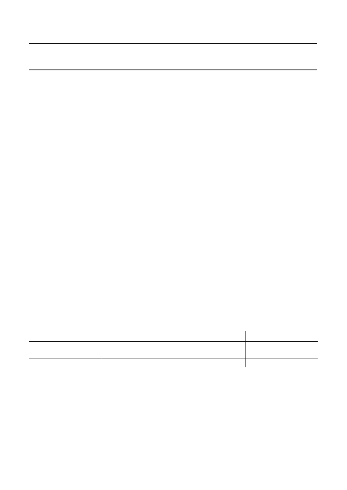
Table 1 Differences between TSA5526 and TSA5527
TYPE NUMBER DATA WORD REFERENCE DIVIDER FREQUENCY STEP (kHz)
TSA5526 18-bit 512
TSA5526 19-bit 1024
TSA5527 19-bit 640
Notes
1. The selection of the reference divider is given by an automatic identification of the data word length.
2. The reference divider is set to 640 at power-on reset.
1996 Sep 24 4
(1)
(2)
(1)
62.5
31.25
50
Page 5
Philips Semiconductors Product specification
1.3 GHz universal bus-controlled
TV synthesizers
BLOCK DIAGRAM
tune
CP
V
9
10
AMP
CP
PUMP
CHARGE
PHASE
DIGITAL
COMPARATOR
T2,T1,T0
LOGIC
IN-LOCK
DETECTOR
lock
CC1
V
3
OS
RSA,RSB
EE
V
2
REGISTER
7-BIT CONTROL
LOCK/
12
T2,T1,T0
TSA5526; TSA5527
ADC
MBE327
div
ref
f
f
15-BIT
DIVIDER
PROGRAMMABLE
DIVIDER
DIVIDE-BY-8
PRESCALER
1
RF
handbook, full pagewidth
512/640/1024
XTAL
OSCILLATOR
16
XTAL
REGISTER
15-BIT FREQUENCY
RSA RSB
RESET
POWER-ON
2
I C/3-WIRE BUS
14
13
SCL
SDA
GATE
REGISTER
4-BIT BAND SWITCH
TRANSCEIVER
15
CE
11
5-LEVEL
SW
ADC
5
6
7
8
4
TSA5526
TSA5527
BS4
BS3
BS2
BS1
CC2
V
Fig.1 Block diagram.
1996 Sep 24 5
Page 6
Philips Semiconductors Product specification
1.3 GHz universal bus-controlled
TV synthesizers
PINNING
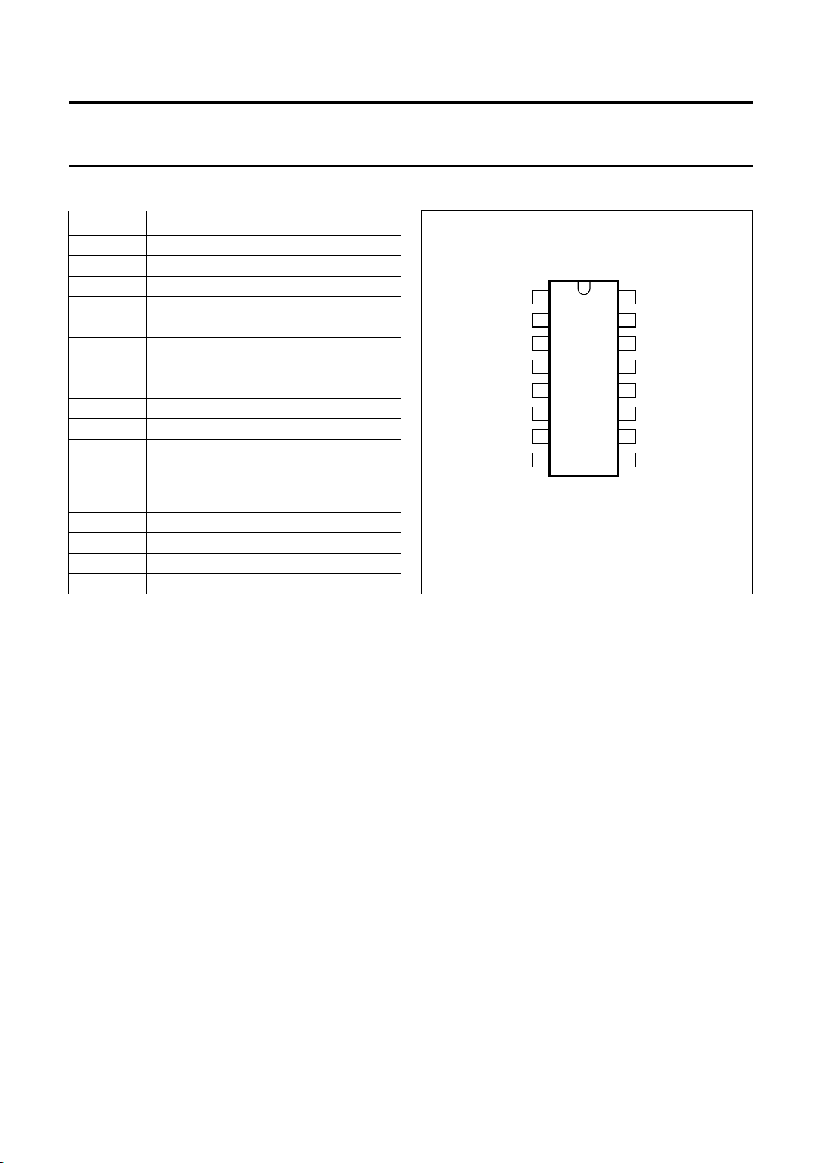
SYMBOL PIN DESCRIPTION
RF 1 RF signal input
V
EE
V
CC1
V
CC2
BS4 5 PNP band switch buffer output 4
BS3 6 PNP band switch buffer output 3
BS2 7 PNP band switch buffer output 2
BS1 8 PNP band switch buffer output 1
CP 9 charge-pump output
V
tune
SW 11 bus format selection input, I
LOCK/ADC 12 lock detector output (3-wire bus/
SCL 13 serial clock input
SDA 14 serial data input/output
CE 15 chip enable/address selection input
XTAL 16 crystal oscillator input
2 ground
3 supply voltage (+5 V)
4 band switch supply voltage (+12 V)
10 tuning voltage output
2
C-bus
or 3-wire
2
ADC input (I
C-bus)
handbook, halfpage
TSA5526; TSA5527
RF
1
V
2
EE
V
3
CC1
V
4
CC2
BS4
BS3
BS2
BS1
Fig.2 Pin configuration.
5
6
7
8
TSA5526
TSA5527
MBE326
XTAL
16
15
CE
14
SDA
SCL
13
12
LOCK/ADC
11
SW
V
10
9
CP
tune
FUNCTIONAL DESCRIPTION
The device is controlled via the I2C-bus or the 3-wire bus
depending on the voltage applied to the SW input (pin 11).
A HIGH level on the SW input enables the 3-wire bus
inputs which are CE (Chip Enable), SDA (serial data input)
and SCL (serial clock input). A LOW level on the SW input
enables the I2C-bus inputs which are AS (Address
Selection input), SDA (serial data input/output) and SCL
(serial clock input). The bus format selection is given in
Table 2.
2
C-bus mode (SW = LOW); see Table 3
I
W
RITE MODE (R/W = 0)
Data bytes can be sent to the device after the address
transmission (first byte). Four data bytes are required to
fully program the device. The bus transceiver has an
auto-increment facility which permits the programming of
the device within one single transmission
(address + 4 data bytes).
The device can also be partially programmed providing
that the first data byte following the address is Divider
Byte 1 (DB1) or the Control Byte (CB). The bits in the data
bytes are defined in Table 3.
The first bit of the first data byte transmitted indicates
whether frequency data (first bit = logic 0) or control and
band switch data (first bit = logic 1) will follow. Until an
2
I
C-bus STOP command is sent by the controller,
additional data bytes can be entered without the need to
readdress the device. The frequency register is loaded
after the 8th clock pulse of the second Divider Byte (DB2),
the control register is loaded after the 8th clock pulse of the
Control Byte (CB) and the band switch register is loaded
after the 8th clock pulse of the Band switch Byte (BB).
2
C-BUS ADDRESS SELECTION
I
The module address contains programmable address bits
(MA1 and MA0) which offer the possibility of having
several synthesizers (up to 3) in one system by applying a
specific voltage to the CE input.
The relationship between MA1 and MA0 and the input
voltage applied to the CE input is given in Table 5.
1996 Sep 24 6
Page 7
Philips Semiconductors Product specification
1.3 GHz universal bus-controlled
TSA5526; TSA5527
TV synthesizers
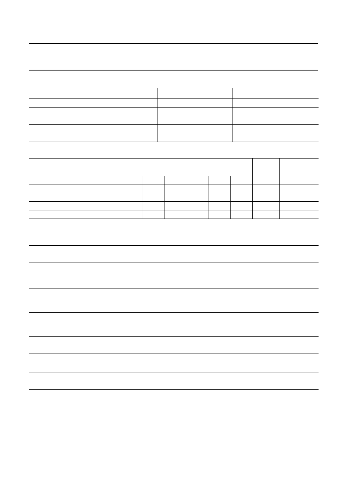
Table 2 Bus format selection
PIN NAME 3-WIRE BUS MODE I
11 SW OPEN or HIGH LOW
12 LOCK/ADC LOCK/TEST output ADC input/TEST output
13 SCL clock input SCL input
14 SDA data input SDA input/output
15 CE chip enable input address selection input
2
Table 3 I
C-bus data format
BYTE MSB DATA BYTE LSB
Address Byte (ADB) 1 1000MA1MA0R/W=0 A
Divider Byte 1 (DB1) 0 N14 N13 N12 N11 N10 N9 N8 A
Divider Byte 2 (DB2) N7 N6 N5 N4 N3 N2 N1 N0 A
Control Byte (CB) 1 CP T2 T1 T0 RSA RSB OS A
Band switch Byte (BB) X X X X BS4 BS3 BS2 BS1 A
2
C-BUS MODE
SLAVE
ANSWER
Table 4 Description of Table 3
SYMBOL DESCRIPTION
A acknowledge
MA1 and MA0 programmable address bits (see Table 5)
14
N14 to N0 programmable divider bits; N = N14 × 2
+ N13 × 213+...+N1×2+N0
CP charge-pump current; CP = 0 = 60 µA; CP = 1 = 280 µA (default)
T2 to T0 test bits (see Table 6); for normal operation T2 = 0, T1 = 0 and T0 = 1 (default)
RSA and RSB reference divider ratio select bits (see Table 7)
OS tuning amplifier control bit; for normal operation OS = 0 and tuning voltage is ON (default);
when OS = 1 tuning voltage is OFF (high impedance)
BS4 to BS1 PNP band switch buffers control bits; when BS
= 0 buffer n is OFF; when BSn= 1 buffer n
n
is ON
X don’t care
2
Table 5 I
C-bus address selection
VOLTAGE APPLIED TO THE CE INPUT (SW = LOW) MA1 MA0
0 V to 0.1V
CC1
00
Always valid 0 1
0.4V
0.9V
CC1
CC1
to 0.6V
to V
CC1
CC1
10
11
1996 Sep 24 7
Page 8
Philips Semiconductors Product specification
1.3 GHz universal bus-controlled
TSA5526; TSA5527
TV synthesizers
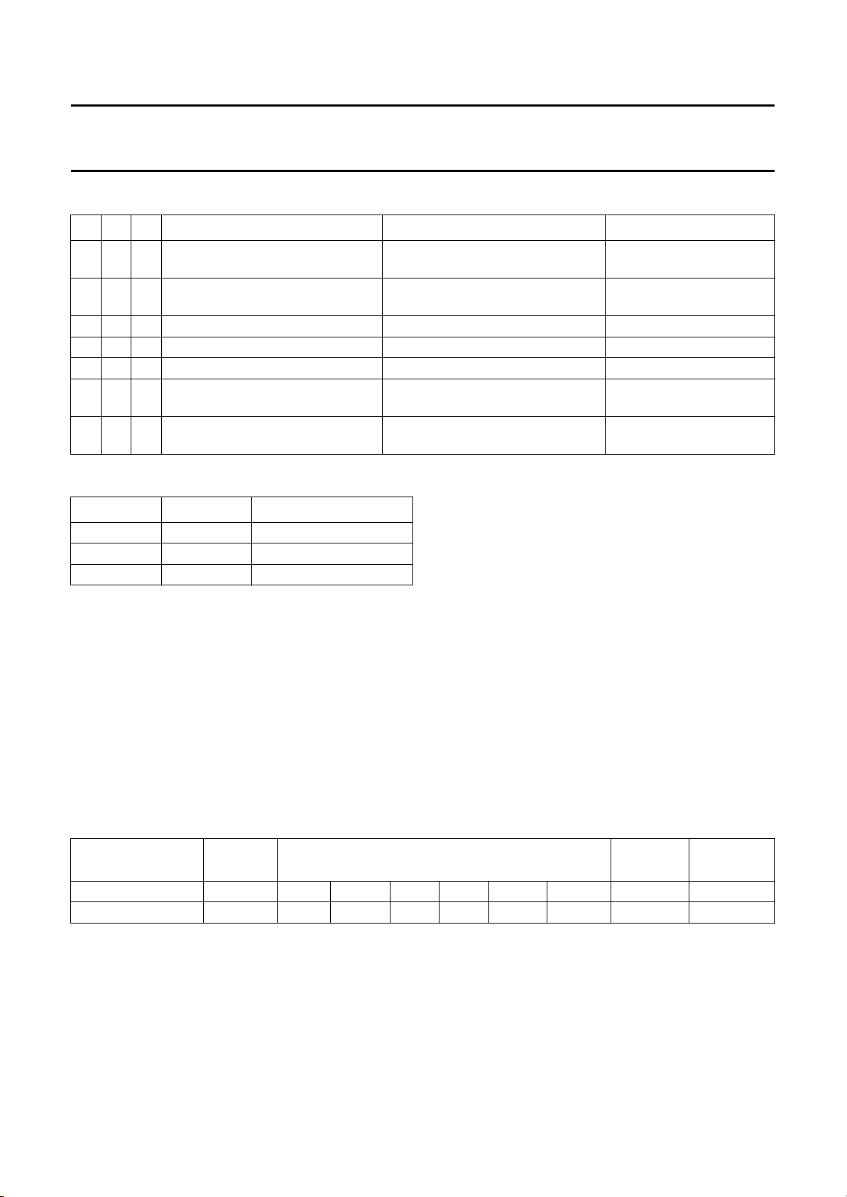
Table 6 Test bits
T2 T1 T0 TSA5526; TSA5527 TSA5526A; TSA5527A REMARKS
0 0 0 normal operation with automatic
charge-pump switch ON
0 0 1 normal operation with automatic
charge-pump switch OFF
0 1 X charge-pump is OFF charge-pump is OFF
1 1 0 charge-pump is sinking current charge-pump is sinking current
1 1 1 charge-pump is sourcing current charge-pump is sourcing current
100f
101
is available at LOCK output f
ref
1
⁄2f
is available at LOCK output
div
Table 7 Ratio select bits
RSA RSB REFERENCE DIVIDER
X 0 640
0 1 1024
1 1 512
automatic charge-pump switch OFF
automatic charge-pump switch ON status at POR
is available at LOCK output the ADC cannot be used
ref
when test mode is active
1
⁄2f
is available at LOCK output the ADC cannot be used
div
when test mode is active
The device will then release the data line to allow the
microcontroller to generate a stop condition. The POR flag
is set to logic 1 at power-on. The flag is reset when an
end-of-data is detected by the device (end of a read
sequence). Control of the loop is made possible with the
in-lock flag (FL) which indicates when the loop is locked
(FL = logic 1).
EAD MODE (R/W = LOGIC 1); see Table 8
R
Data can be read from the device by setting the R/W bit to
logic 1. After the slave address has been recognized, the
device generates an acknowledge pulse and the first data
byte (status byte) is transferred on the SDA line (MSB
first). Data is valid on the SDA line during a HIGH level of
the SCL clock signal. A second data byte can be read from
the device if the microcontroller generates an
acknowledge on the SDA line (master acknowledge).
End of transmission will occur if no master acknowledge
The Automatic Charge-Pump Switch flag (ACPS) is LOW
when the automatic charge-pump switch mode is ON and
the loop is locked. In other conditions ACPS = logic 1.
When ACPS = logic 0, the charge-pump current is forced
to the LOW value.
A built-in ADC is available at pin 12 (I2C-bus only).
This converter can be used to apply AFC information to the
microcontroller from the IF section of the television.
The relationship between the bits A2 to A0 is given in
Table 9.
occurs.
Table 8 Read data format
BYTE MSB DATA BYTE LSB
ANSWER
Address Byte (ADB) 1 1 0 0 0 MA1 MA0 R/W = 1 A
Status Byte (SB) POR
(2)
FL
(3)
ACPS
(4)
11A2
(5)
A1
(5)
A0
(5)
Notes
1. A = acknowledge.
2. POR = power-on reset flag (POR = logic 1 at power-on).
3. FL = in-lock flag (FL = logic 1 when the loop is locked).
4. ACPS = automatic charge-pump switch flag (active ACPS = logic 0; non-active ACPS = logic 1).
5. A2 to A0 = digital outputs of the 5-level ADC.
SLAVE
(1)
−
1996 Sep 24 8
Page 9
Philips Semiconductors Product specification
1.3 GHz universal bus-controlled
TV synthesizers
Table 9 ADC levels
VOLTAGE APPLIED
AT ADC INPUT
CC1
CC1
CC1
CC1
to V
to 0.6V
to 0.45V
to 0.3V
CC1
0.6V
0.45V
0.3V
0.15V
0 to 0.15V
(1)
CC1
CC1
CC1
CC1
Note
1. Accuracy is ±0.03V
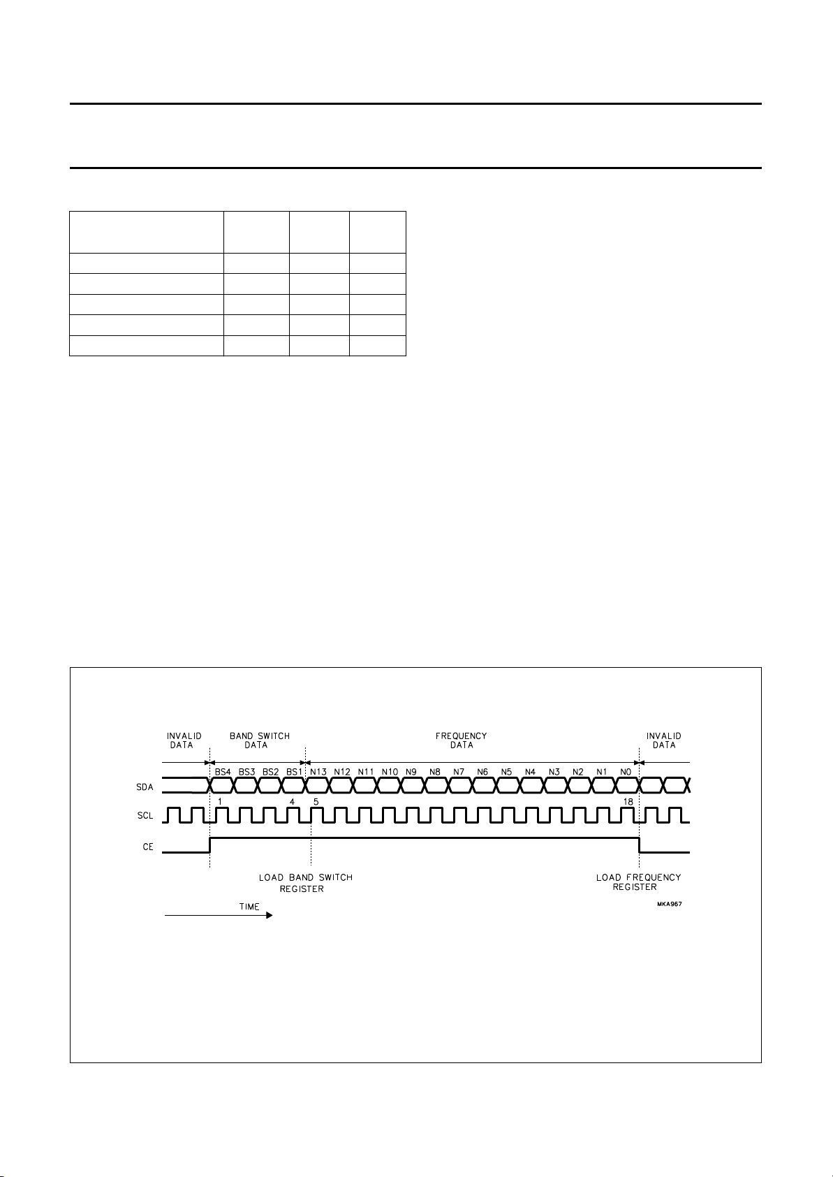
CC1
3-wire bus mode (SW = open-circuit or V
see Figs 3, 4 and 5
During a HIGH level on the CE input, the data is clocked
into the data register at the HIGH-to-LOW transition of the
clock pulse. The first four bits control the band switch
buffers and are loaded into the internal band switch
register on the 5th rising edge of the clock pulse.
The frequency bits are loaded into the frequency register
at the HIGH-to-LOW transition of the chip enable line when
an 18-bit or 19-bit data word is transmitted.
At power-on the charge-pump current is set to 280 µA, the
tuning voltage output is disabled (V
A2 A1 A0
100
011
010
001
000
.
);
CC1
= 33 V in
tune
TSA5526; TSA5527
application; see Fig.12), the test bits T2, T1 and T0 are set
to the 0 0 1 state in the normal mode with ACPS OFF for
TSA55226; TSA5527 and ACPS ON for TSA5526A;
TSA5527A. RSB is set to logic 1 (TSA5526) or logic 0
(TSA5527). When an 18-bit data word is transmitted, the
most significant bit of the divider N14 is internally set to
logic 0 and bit RSA is set to logic 1. When a 19-bit data
word is transmitted, bit RSA is set to logic 0.
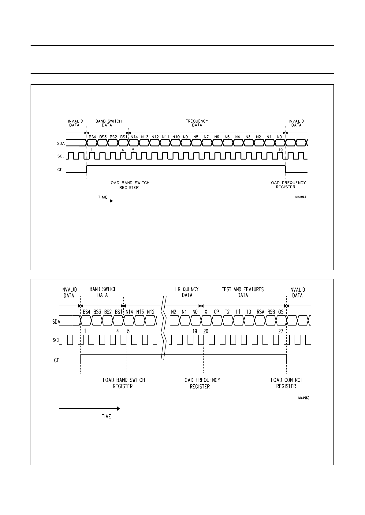
When a 27-bit word is transmitted, the frequency bits are
loaded into the frequency register on the 20th rising edge
of the clock pulse and the control bits at the HIGH-to-LOW
transition of the chip enable line. In this mode, the
reference divider is given by the RSA and RSB bits
(see Table 7). The test bits T2, T1 and T0, the
charge-pump bit CP, the ratio select bit RSB and the
OS bit can only be selected or changed with a 27-bit
transmission. They remain programmed if an 18-bit or a
19-bit transmission occurs. Only RSA is controlled by the
transmission length when the 18-bit or 19-bit format is
used.
A data word of less than 18 bits will not affect the
frequency register of the device. The definition of the bits
is unchanged compared to the I2C-bus mode.
The power-on detection threshold voltage V
V
= 2 V at room temperature. Below this threshold, the
CC1
device is reset to the power-on state previously described.
is fixed to
POR
For TSA5526 bit RSB =logic 1 at power-on; the reference divider is 512 or 1024.
For TSA5527 bit RSB =logic 0 at power-on; the reference divider is 640.
For TSA5526 and TSA5527 the value of RSB can also be programmed by using the 27-bit data format. When returning to the normal mode, bit RSB
remains as programmed with the 27-bit data word.
1996 Sep 24 9
Fig.3 Normal mode; 18-bit data format (RSA = 1).
Page 10
Philips Semiconductors Product specification
1.3 GHz universal bus-controlled
TSA5526; TSA5527
TV synthesizers
For TSA5526 bit RSB =1 at power-on; the reference divider is 512 or 1024.
For TSA5527 bit RSB = 0 at power-on; the reference divider is 640.
For TSA5526/TSA5527 the value of RSB can also be programmed by using the 27-bit data format. When returning to the normal mode, bit RSB remains
as programmed with the 27-bit data word.
Fig.4 Normal mode; 19-bit data format (RSA = 0).
For TSA5526 bit RSB = 1 at power-on; the reference divider is 512 or 1024.
For TSA5527 bit RSB = 0 at power-on; the reference divider is 640.
For TSA5526/TSA5527 the value of RSB can also be programmed by using the 27-bit data format. When returning to the normal mode, bit RSB remains
as programmed with the 27-bit data word.
1996 Sep 24 10
Fig.5 Test and features mode; 27-bit data format.
Page 11
Philips Semiconductors Product specification
1.3 GHz universal bus-controlled
TSA5526; TSA5527
TV synthesizers
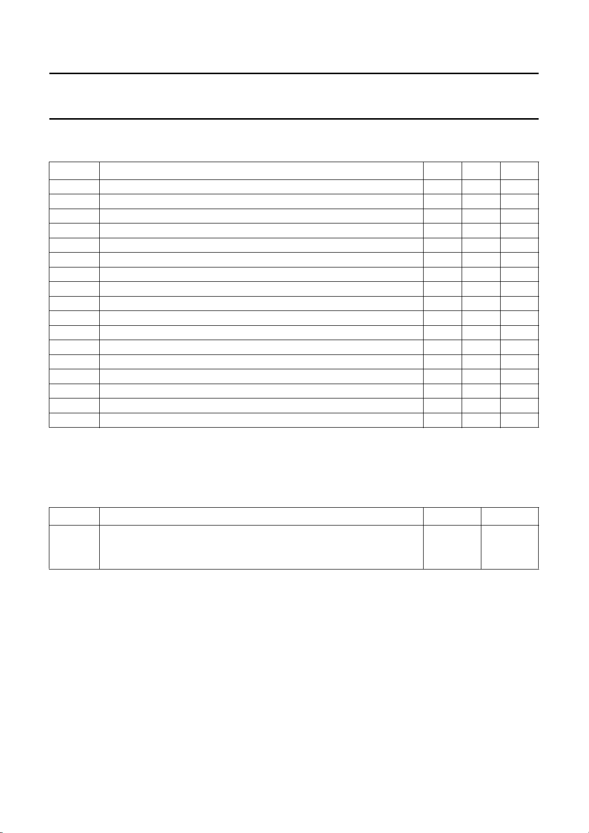
LIMITING VALUES
In accordance with the Absolute Maximum Rating System (IEC 134).
SYMBOL PARAMETER MIN. MAX. UNIT
V
CC1
V
CC2
V
i(RF)
V
o(BSn)
I
o(BSn)
V
o(CP)
V
o(tune)
V
i(SW)
V
o(LOCK)
V
i(SCL)
V
i/o(SDA)
I
o(SDA)
V
i(CE)
V
i(xtal)
T
stg
T
j
t
sc
supply voltage; +5 V (pin 3) −0.3 +6.0 V
band switch supply voltage; +12 V (pin 4) −0.3 +16 V
prescaler input voltage (pin 1) −0.3 V
band switch buffers output voltage (pins 5 to 8) −0.3 V
CC1
CC2
V
V
band switch buffers output current −1 +50 mA
charge-pump output voltage (pin 9) −0.3 V
CC1
V
output tuning voltage (pin 10) −0.3 +35 V
input switching voltage (pin 11) −0.3 V
lock output voltage (pin 12) −0.3 V
CC1
CC1
V
V
serial clock input voltage (pin 13) −0.3 +6.0 V
serial data input/output voltage (pin 14) −0.3 +6.0 V
serial data output current −1 +10 mA
chip enable input voltage (pin 15) −0.3 +6.0 V
crystal oscillator input voltage (pin 16) −0.3 V
CC1
V
storage temperature −40 +150 °C
maximum junction temperature − +150 °C
short-circuit time; every pin except pin 4 to pin 3 and every pin to pin 2; note 1 − 10 s
Note
1. Short-circuit between V
rating at V
CC1
.
CC1
and V
is allowed provided the voltage applied to V
CC2
is less than the 6 V maximum
CC2
THERMAL CHARACTERISTICS
SYMBOL P ARAMETER V ALUE UNIT
R
th j-a
thermal resistance from junction to ambient in free air
SO16 110 K/W
SSOP16 142 K/W
HANDLING
Inputs and outputs are protected against electrostatic discharge in normal handling. However, to be totally safe, it is
desirable to take normal precautions appropriate to handling bipolar devices. Every pin withstands the ESD test in
accordance with
“MIL-STD-883C
” category B (2000 V). Every pin withstands the ESD test in accordance with Philips
Semiconductors Machine Model 0 Ω, 200 pF (200 V).
1996 Sep 24 11
Page 12
Philips Semiconductors Product specification
1.3 GHz universal bus-controlled
TSA5526; TSA5527
TV synthesizers
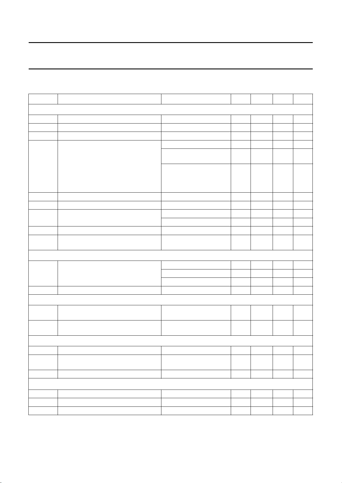
CHARACTERISTICS
V
= 4.5 to 5.5 V; V
CC1
CC2=VCC1
SYMBOL PARAMETER CONDITIONS MIN. TYP. MAX. UNIT
Supplies
V
V
I
CC1
I
CC2
V
f
RF
CC1
CC2
POR
supply voltage 4.5 − 5.5 V
band switch buffers supply voltage V
supply current at power-on − 20 25 mA
band switch buffers supply current at power-on − 0.5 1.0 mA
supply voltage below which POR is active 1.5 2.0 − V
RF input frequency 64 − 1300 MHz
DR divider ratio 15-bit frequency word 256 − 32767
f
Z
xtal
xtal
crystal oscillator input frequency R
crystal oscillator input impedance
(absolute value)
to 13.2 V; T
= −20 to +85 °C; unless otherwise specified.
amb
one band switch buffer is
source
=40mA
ON; I
two band switch buffers are
ON;
=40mA+5mA
I
source
(any combination)
14-bit frequency word 256 − 16383
=25to300Ω 3.2 4 4.48 MHz
xtal
fi= 4 MHz 600 1200 −Ω
− 13.5 V
CC1
− 50 55 mA
− 56 62 mA
Prescaler (see Figs 6 and 7)
V
Z
i(RF)
i(RF)
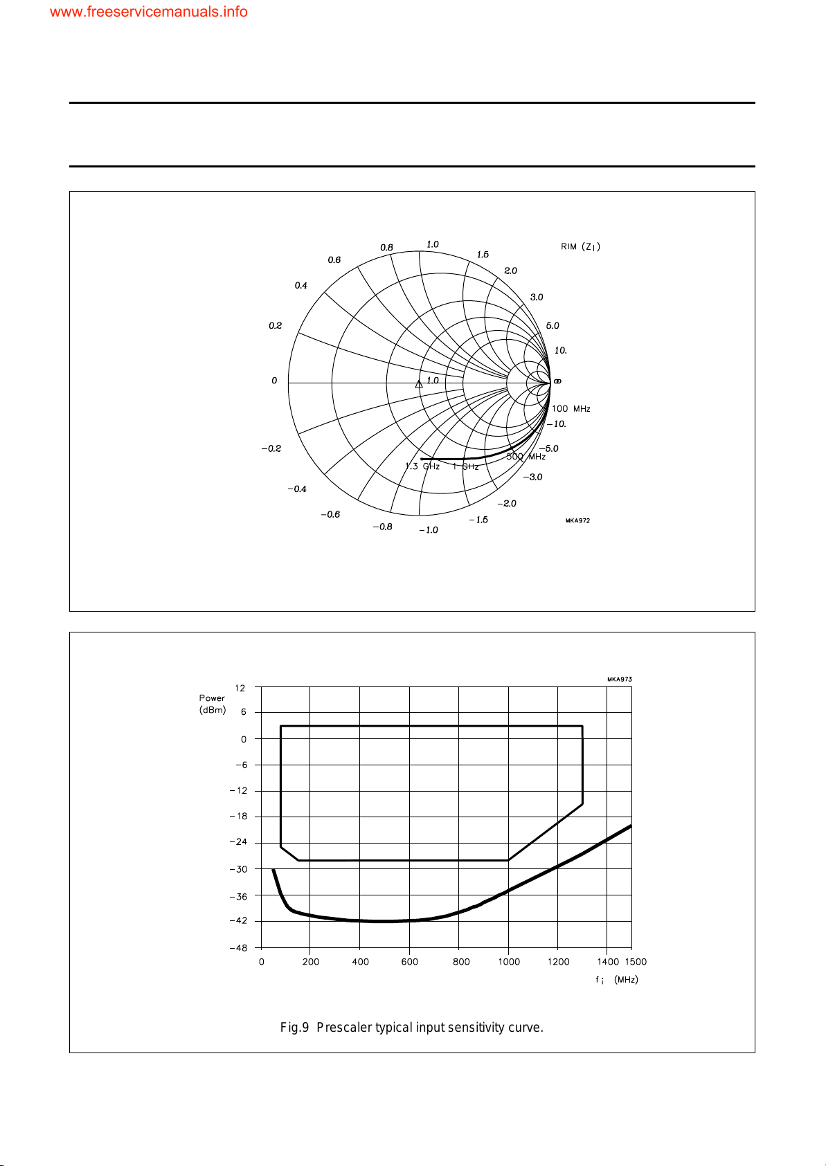
RF input level fi= 80 to 150 MHz −25 − 3 dBm
= 150 to 1000 MHz −28 − 3 dBm
f
i
= 1000 to 1300 MHz −15 − 3 dBm
f
i
input impedance see Fig.8
PNP band switch buffers outputs (pins 5 to 8)
I
LO
output leakage current V
CC2
= 13.5 V;
Vo=0V
V
o(sat)
output saturation voltage I
= 40 mA;
source
V
o(sat)=VCC2
LOCK output (PNP collector output) 3 wire bus mode (pin 12)
I
o(ool)
V
osat(ool)
V
o(LOCK)
ADC input (I
V
i(ADC)
I
IH(ADC)
I
IL(ADC)
output current when out-of-lock V
output saturation voltage when
out-of-lock
= 5.5 V; Vo= 5.5 V −− 100 µA
CC1
I
= 200 µA;
source
V
o(sat)=VCC1
lock output voltage − 0.01 0.4 V
2
C-bus mode) pin 12
ADC input voltage see Table 9 0 − V
HIGH level input current V
LOW level input current V
ADC=VCC1
=0V −10 −−µA
ADC
− V
− V
−10 −−µA
− 0.2 0.4 V
o
− 0.4 0.8 V
o
V
CC1
−− 10 µA
1996 Sep 24 12
Page 13
Philips Semiconductors Product specification
1.3 GHz universal bus-controlled
TSA5526; TSA5527
TV synthesizers
SYMBOL PARAMETER CONDITIONS MIN. TYP. MAX. UNIT
SW input (bus format switch)
V
IL
V
IH
I
IH
I
IL
CE input (chip enable/address selection)
V
IL
V
IH
I
IH
I
IL
SCL and SDA inputs
V
IL
V
IH
I
IH
I
IL
f
clk
SDA outputs (I
I
LO
V
o
Charge-pump output CP
|I
ICPH
|I
ICPL
V
CP
I
LI(off)
Tuning voltage output V
I
LO(off)
V
o
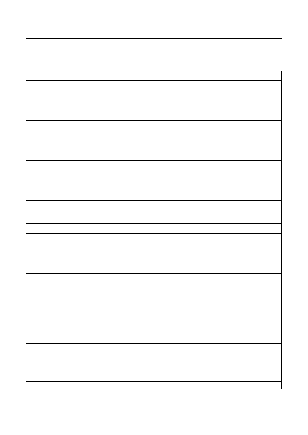
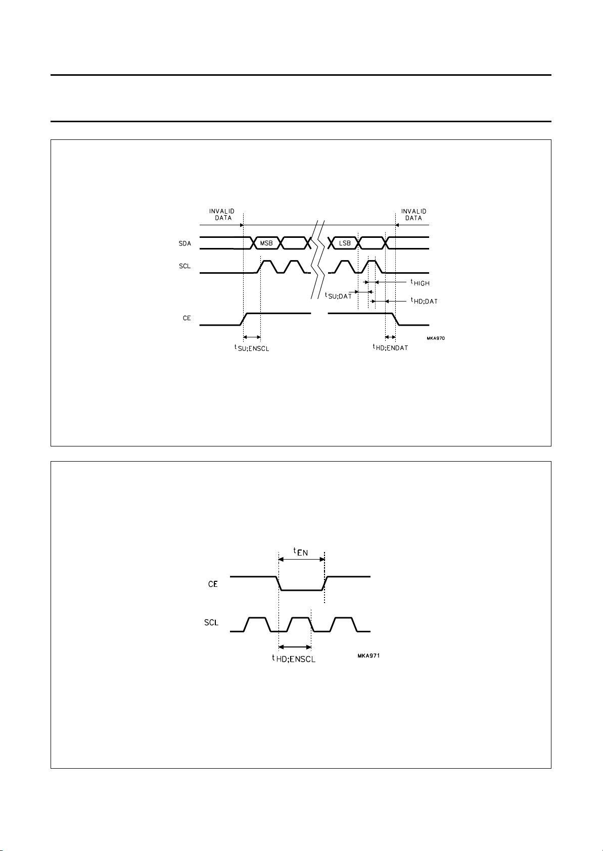
3-wire bus timing (see Figs 6 and 7)
t
HIGH
t
SU;DAT
t
HD;DAT
t
SU;ENSCL
t
HD;ENDAT
t
EN
t
HD;ENSCL
LOW level input voltage 0 − 1.5 V
HIGH level input voltage 3 − V
HIGH level input current VSW=V
CC1
−− 10 µA
CC1
V
LOW level input current VSW=0V −100 −−µA
LOW level input voltage 0 − 1.5 V
HIGH level input voltage 3 − 5.5 V
HIGH level input current VCE= 5.5 V −− 10 µA
LOW level input current VCE=0V −10 −−µA
LOW level input voltage 0 − 1.5 V
HIGH level input voltage 3.0 − 5.5 V
HIGH level input current V
LOW level input current V
BUS
V
BUS
BUS
V
BUS
= 5.5 V; V
= 5.5 V; V
= 1.5 V; V
=0V; V
CC1
=0V −− 10 µA
CC1
= 5.5 V −− 10 µA
CC1
=0V −− 10 µA
CC1
= 5.5 V −10 −−µA
clock frequency − 100 400 kHz
2
C-bus mode)
output leakage current V
output voltage I
= 5.5 V −− 10 µA
SDA
=3mA −− 0.4 V
sink
| HIGH charge-pump current CP = 1 − 280 −µA
| LOW charge-pump current CP = 0 − 60 −µA
output voltage in-lock; T
=25°C − 1.95 − V
amb
off-state leakage current T2 = 0; T1 = 1 −15 −0.5 +15 nA
tune
leakage current when switched-off OS = 1; V
output voltage when the loop is closed OS = 0; T2 = 0; T1 = 0;
=33V −− 10 µA
tune
0.2 − 32.7 V
T0 = 1; RL=27kΩ;
V
=33V
tune
clock high time 2 −−µs
data set-up time 2 −−µs
data hold time 2 −−µs
enable to clock set-up time 10 −−µs
enable to data hold time 2 −−µs
enable between two transmissions 10 −−µs
enable to clock active edge hold time 6 −−µs
1996 Sep 24 13
Page 14
Philips Semiconductors Product specification
1.3 GHz universal bus-controlled
TV synthesizers
TSA5526; TSA5527
Fig.6 Timing diagram for 3-wire bus; SDA, SCL and CE.
1996 Sep 24 14
Fig.7 Timing diagram for 3-wire bus; CE and SCL.
Page 15
Philips Semiconductors Product specification
BBBBBBBBBBBBBBBBBBBBBBBBBB
B
B
B
B
B
B
B
B
B
B
B
B
B
B
B
B
B
BBBBBBBBBBBBBBBBBBBBBBBBBB
1.3 GHz universal bus-controlled
TV synthesizers
TSA5526; TSA5527
Fig.8 Prescaler Smith chart of typical input impedance at pin 1.
BBBBBBBBBBBBBBBBBBBBBBBBB
BBBBBBBBBBBBBBBBBBBBBBBBB
BBBBBBBBBBBBBBBBBBBBBBBBB
BBBBBBBBBBBBBBBBBBBBBBBBB
BBBBBBBBBBBBBBBBBBBBBBBBB
BBBBBBBBBBBBBBBBBBBBBBBBB
BBBBBBBBBBBBBBBBBBBBBBBBB
BBBBBBBBBBBBBBBBBBBBBBBBB
BBBBBBBBBBBBBBBBBBBBBBBBB
BBBBBBBBBBBBBBBBBBBBBBBBB
BBBBBBBBBBBBBBBBBBBBBBBBB
BBBBBBBBBBBBBBBBBBBBBBBBB
BBBBBBBBBBBBBBBBBBBBBBBBB
BBBBBBBBBBBBBBBBBBBBBBBBB
BBBBBBBBBBBBBBBBBBBBBBBBB
BBBBBBBBBBBBBBBBBBBBBBBBB
BBBBBBBBBBBBBBBBBBBBBBBBB
Fig.9 Prescaler typical input sensitivity curve.
1996 Sep 24 15
Page 16
Philips Semiconductors Product specification
1.3 GHz universal bus-controlled
TV synthesizers
INTERNAL PIN CONFIGURATION
handbook, full pagewidth
V
CC1
1
RF
V
EE
2
V
EE
3
V
CC1
4
V
CC2
V
CC2
5
BS4
V
ref
internal
reference
voltage
to address
selection
TSA5526; TSA5527
V
CC1
16
XTAL
V
EE
V
CC1
15
CE
V
EE
V
CC1
14
SDA
BS3
BS2
BS1
V
ACK
2
V
EE
V
CC2
(I C BUS)
TSA5526
6
V
EE
V
CC2
7
V
EE
V
CC2
8
TSA5527
command
down
EE
V
CC1
13
SCL
V
EE
V
CC1
12
LOCK/ADC
V
EE
V
CC1
11
SW
V
EE
10
V
tune
V
EE
V
CC1
9
CP
1996 Sep 24 16
V
EE
up
V
EE
MGD635
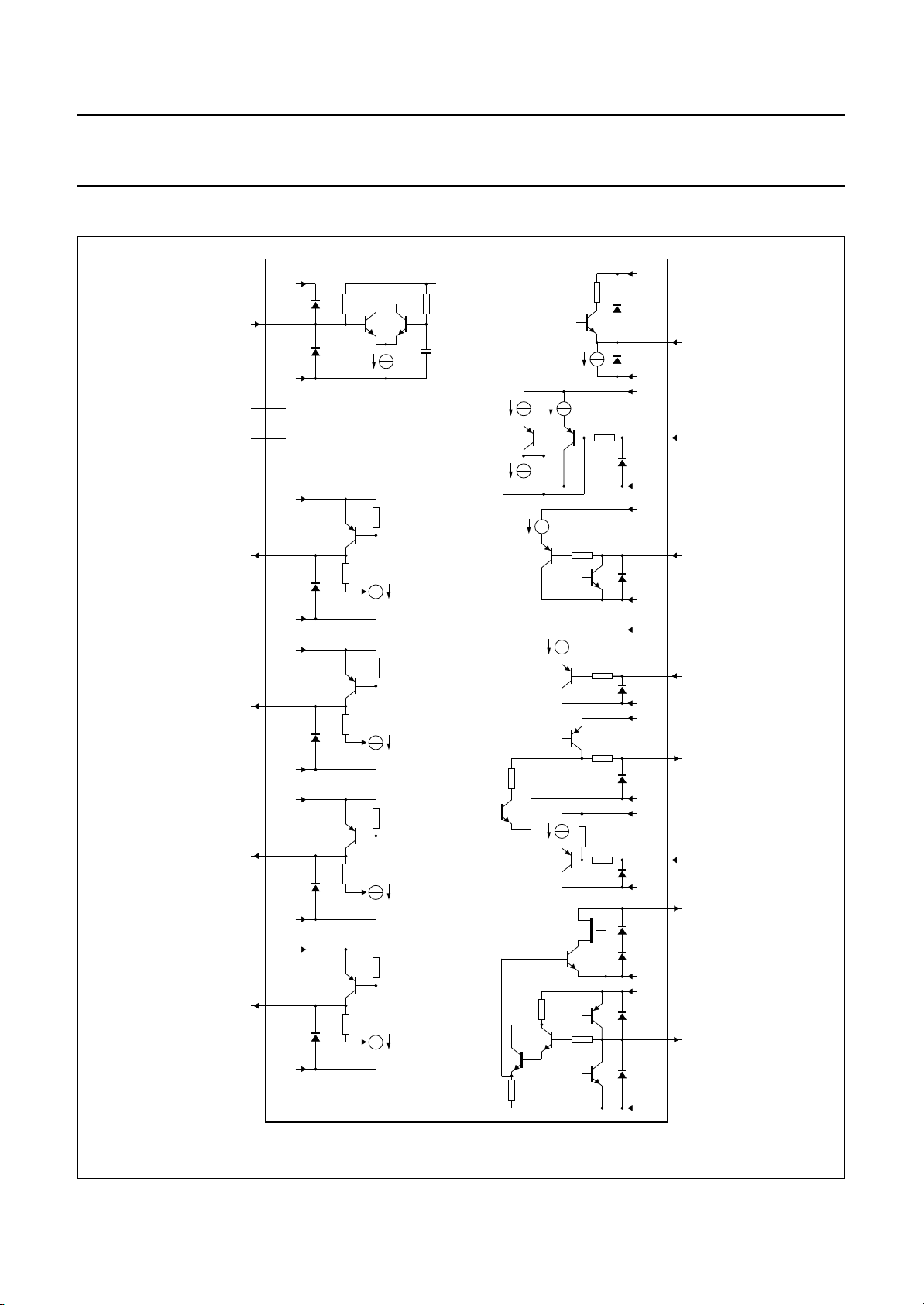
Fig.10 Internal pin configuration.
Page 17
Philips Semiconductors Product specification
1.3 GHz universal bus-controlled
TSA5526; TSA5527
TV synthesizers
APPLICATION INFORMATION
Tuning amplifier
The tuning amplifier is capable of driving the varicap
voltage without an external transistor. The tuning voltage
output must be connected to an external load of 27 kΩ
which is connected to the tuning voltage supply rail.
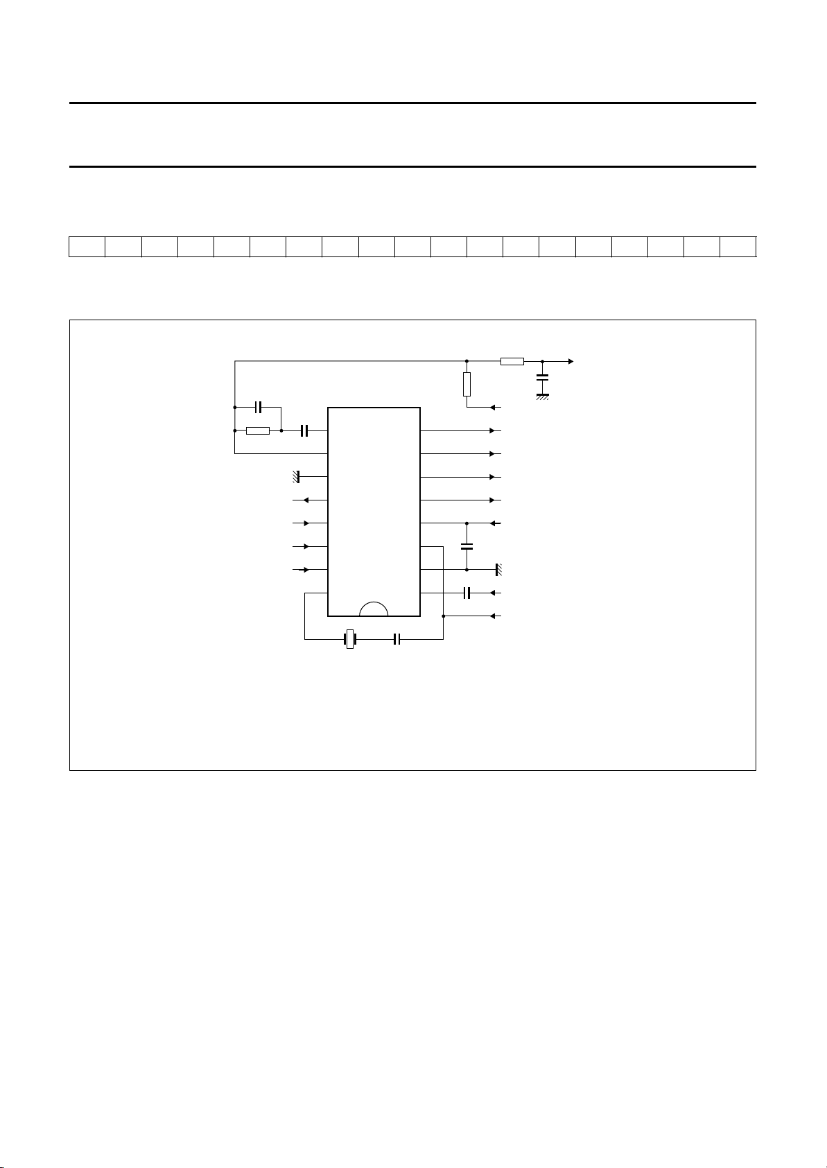
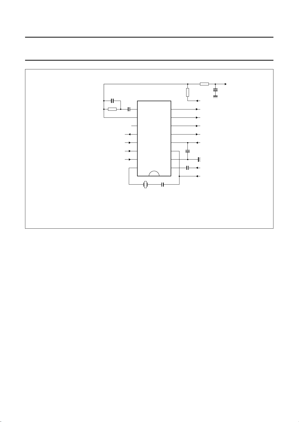
Figs 11 and 12 show a possible loop filter. The component
values depend on the oscillator characteristics and the
selected reference frequency.
2
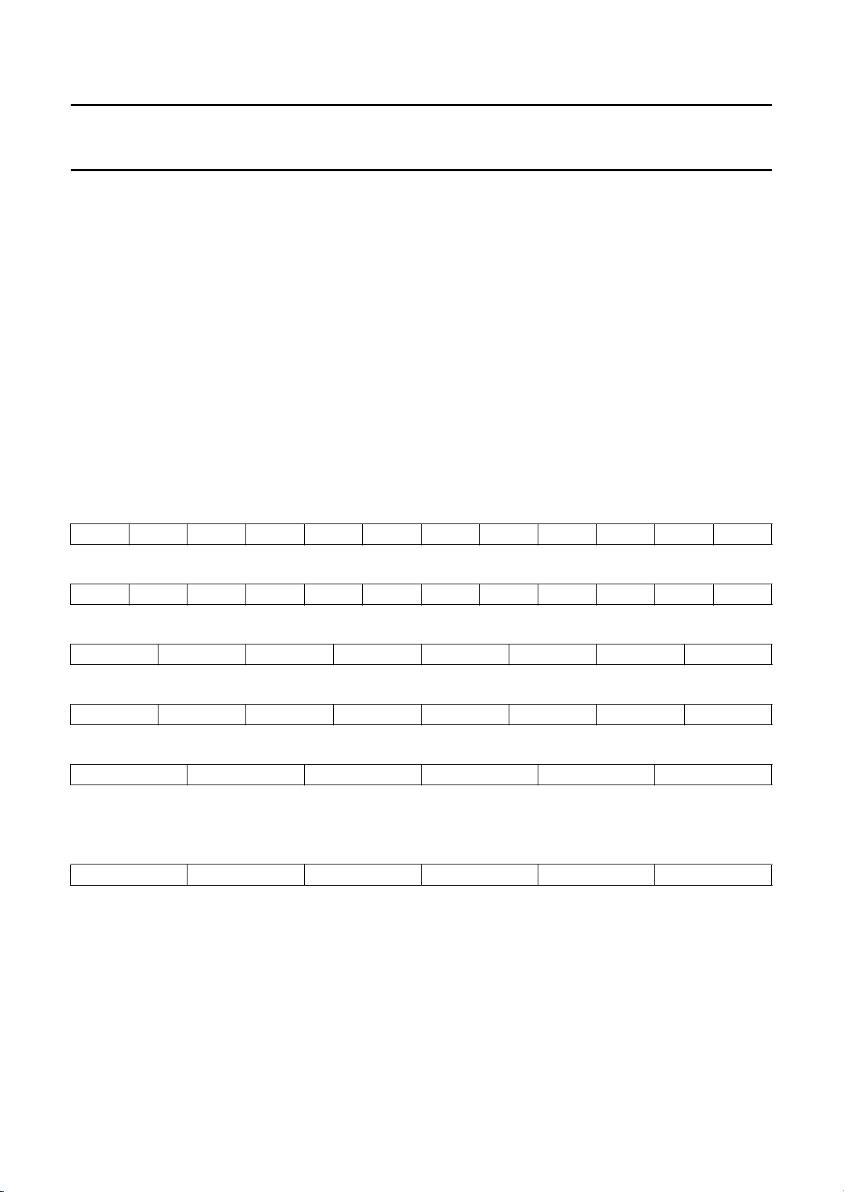
Examples of I
Tables 10 to 14 show the various sequences where f
S = START, A = acknowledge and P = STOP. The sequence is as follows:
START + address byte + divider byte 1 + divider byte 2 + control byte + band switch byte + STOP.
For the complete sequence see Table 10 (sequence 1) or Table 11 (sequence 2).
Table 10 Complete sequence 1
SC2A06A40ACEA08A P
C-bus sequences (SW = LOW)
osc
Crystal oscillator
The crystal oscillator uses a 4 MHz crystal connected in
series with an 18 pF capacitor thereby operating in the
series resonance mode. Connecting the oscillator to the
supply voltage is preferred but it can, however, also be
connected to ground.
= 100 MHz, BS4 = ON, ICP= 280 µA, N = 512, f
xtal
= 4 MHz,
Table 11 Complete sequence 2
SC2ACEA08A06A40A P
Table 12 Divider bytes only sequence
SC2A06A40A P
Table 13 Control and band switch bytes only sequence
SC2ACEA08AP
Table 14 Control byte only sequence
SC2ACEA P
Other sequences are not allowed in the write mode.
Table 15 One status byte acquisition
SC3AXX
Notes
1. XX = the read status byte.
2. X = no acknowledge from the master means end of sequence.
(1)
(2)
X
P
1996 Sep 24 17
Page 18
Philips Semiconductors Product specification
1.3 GHz universal bus-controlled
TSA5526; TSA5527
TV synthesizers
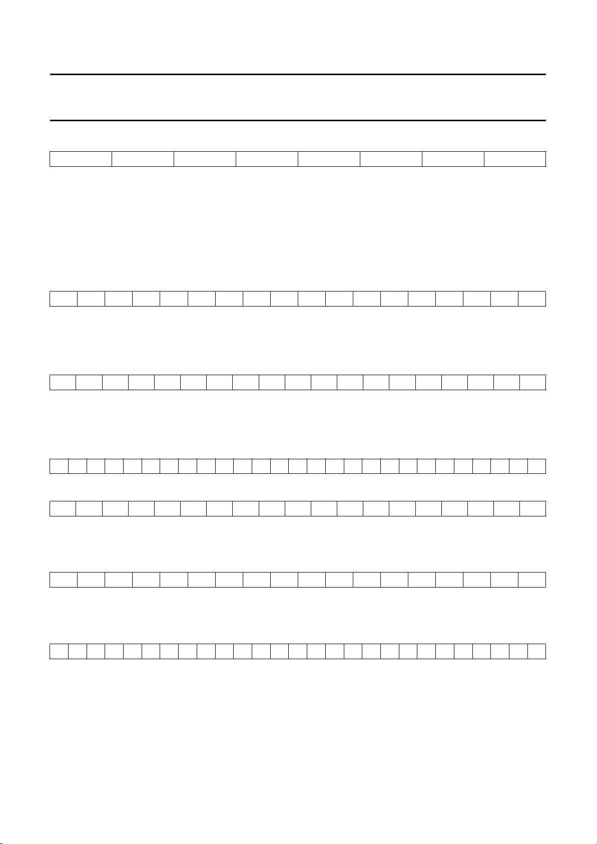
Table 16 Two status byte acquisition
SC3AXX
(1)
AXX
Notes
1. XX = the read status byte.
2. X = no acknowledge from the master means end of sequence.
2
Other I
C-bus addresses may be selected by applying an appropriate voltage to the CE input.
Examples of 3-wire bus sequences (TSA5526; SW = OPEN)
Table 17 18-bit sequence (f
= 800 MHz, BS4 = ON)
osc
100011001000000000
The reference divider is automatically set to 512 unless RSB has been programmed to 0 during a 27-bit sequence
(see Table 19).
Table 18 19-bit sequence (f
= 650 MHz, BS3 = ON)
osc
0100101000101000000
(1)
(2)
X
P
The reference divider is automatically set to 1024 unless RSB has been programmed to 0 during a 27-bit sequence
(see Table 19).
Table 19 27-bit sequence (f
= 750 MHz, BS1 = ON, N = 640, Icp=60µA, no test function)
osc
000101110101001100010001000
Table 20 19-bit sequence
0001010111011100000
This sequence will program f
to 600 MHz in 50 kHz steps. ICP remains at 60 µA.
osc
Table 21 18-bit sequence
000110111011100000
This sequence will program f
Table 22 27-bit sequence (f
to 600 MHz in 50 kHz steps. ICP remains at 60 µA.
osc
= 650 MHz, BS1 = ON)
osc
000110100010100000011001010
This sequence sets RSA to 0, RSB to 1 and CP to 1. After this sequence I
= 280 µA, N = 1024 (19-bit transmission)
CP
and N = 512 (18-bit transmission), RSB = 1.
1996 Sep 24 18
Page 19
Philips Semiconductors Product specification
1.3 GHz universal bus-controlled
TSA5526; TSA5527
TV synthesizers
Example of 3-wire bus sequence (TSA5527; SW = OPEN)
Table 23 19-bit sequence (f
0100011011010110000
N = 640 unless RSB has been programmed to 0 during a 27-bit sequence.
handbook, full pagewidth
= 700 MHz, BS3 = ON)
osc
2.2 nF
100 nF
22 kΩ
SCL
SDA
AS
CP SWITCH
V
SW
LOCK
SCL
SDA
CE
XTAL
tune
TSA552X
22 kΩ
27
kΩ
33 V
BS1
BS2
BS3
BS4LOCK
V
CC2
V
CC1
V
EE
RF
(1)
18 pF4 MHz
1 nF
MLC887
10 nF
HIGH
MID
LOW
12 V
(2)
RF
5 V
nF
V
tune
33
(1) Connection to ground is also allowed.
(2) Capacitor prevents parasitic oscillation on the V
CC2
line.
Fig.11 Typical I2C-bus application.
1996 Sep 24 19
Page 20
Philips Semiconductors Product specification
1.3 GHz universal bus-controlled
TV synthesizers
handbook, full pagewidth
2.2 nF
100 nF
22 kΩ
CLOCK
DATA
ENABLE
TSA5526; TSA5527
22 kΩ
27
kΩ
33 V
CP SWITCH
V
tune
SW
LOCK
TSA552X
SCL
SDA
CE
XTAL
BS1
BS2
BS3
BS4LOCK
V
CC2
V
CC1
V
EE
RF
(1)
18 pF4 MHz
1 nF
MLC888
10 nF
HIGH
MID
LOW
12 V
(2)
RF
5 V
33
nF
V
tune
(1) Connection to ground is also allowed.
(2) Capacitor prevents parasitic oscillation on the V
line.
CC2
Fig.12 Typical 3-wire bus application.
1996 Sep 24 20
Page 21
Philips Semiconductors Product specification
1.3 GHz universal bus-controlled
TV synthesizers
PACKAGE OUTLINES
SO16: plastic small outline package; 16 leads; body width 3.9 mm
D
c
y
Z
16
9
TSA5526; TSA5527
E
H
E
A
X
v M
SOT109-1
A
pin 1 index
4.0
3.8
0.16
0.15
8
b
p
scale
eHELLpQZywv θ
1.27
0.050
1
e
0 2.5 5 mm
DIMENSIONS (inch dimensions are derived from the original mm dimensions)
mm
A
max.
1.75
0.069
A1A2A
0.25
1.45
0.10
1.25
0.0098
0.057
0.0039
0.049
0.25
0.01
b
3
p
0.49
0.25
0.36
0.19
0.0098
0.019
0.0075
0.014
UNIT
inches
Note
1. Plastic or metal protrusions of 0.15 mm maximum per side are not included.
(1)E(1) (1)
cD
10.0
9.8
0.39
0.38
w M
6.2
5.8
0.24
0.23
A
2
1.05
0.041
Q
A
1
detail X
1.0
0.7
0.4
0.6
0.028
0.039
0.020
0.016
(A )
L
p
L
0.25 0.1
0.25
0.01
0.01 0.004
A
3
θ
0.7
0.3
0.028
0.012
o
8
o
0
OUTLINE
VERSION
SOT109-1
1996 Sep 24 21
REFERENCES
IEC JEDEC EIAJ
076E07S MS-012AC
EUROPEAN
PROJECTION
ISSUE DATE
91-08-13
95-01-23
Page 22
Philips Semiconductors Product specification
1.3 GHz universal bus-controlled
TV synthesizers
SSOP16: plastic shrink small outline package; 16 leads; body width 4.4 mm
16
D
c
y
Z
9
E
H
E
TSA5526; TSA5527
SOT369-1
A
X
v M
A
pin 1 index
18
w M
b
b
0.32
0.20
p
p
cD
0.25
5.30
0.13
5.10
0 2.5 5 mm
scale
(1)E(1)
eHELLpQZywv θ
4.5
0.65
4.3
e
DIMENSIONS (mm are the original dimensions)
mm
A
max.
1.5
0.15
0.00
1
A2A
1.4
1.2
3
0.25
UNIT A
Note
1. Plastic or metal protrusions of 0.20 mm maximum per side are not included.
Q
A
2
6.6
6.2
L
0.65
0.45
(A )
L
p
A
1
detail X
0.75
1.0
0.45
3
A
θ
0.130.2 0.1
0.48
0.18
(1)
o
10
o
0
OUTLINE
VERSION
SOT369-1
1996 Sep 24 22
REFERENCES
IEC JEDEC EIAJ
EUROPEAN
PROJECTION
ISSUE DATE
94-04-20
95-02-04
Page 23

Philips Semiconductors Product specification
1.3 GHz universal bus-controlled
TV synthesizers
SOLDERING
Introduction
There is no soldering method that is ideal for all IC
packages. Wave soldering is often preferred when
through-hole and surface mounted components are mixed
on one printed-circuit board. However, wave soldering is
not always suitable for surface mounted ICs, or for
printed-circuits with high population densities. In these
situations reflow soldering is often used.
This text gives a very brief insight to a complex technology.
A more in-depth account of soldering ICs can be found in
our
“IC Package Databook”
Reflow soldering
Reflow soldering techniques are suitable for all SO
packages.
Reflow soldering requires solder paste (a suspension of
fine solder particles, flux and binding agent) to be applied
to the printed-circuit board by screen printing, stencilling or
pressure-syringe dispensing before package placement.
Several techniques exist for reflowing; for example,
thermal conduction by heated belt. Dwell times vary
between 50 and 300 seconds depending on heating
method. Typical reflow temperatures range from
215 to 250 °C.
Preheating is necessary to dry the paste and evaporate
the binding agent. Preheating duration: 45 minutes at
45 °C.
(order code 9398 652 90011).
TSA5526; TSA5527
Wave soldering
Wave soldering techniques can be used for all SO
packages if the following conditions are observed:
• A double-wave (a turbulent wave with high upward
pressure followed by a smooth laminar wave) soldering
technique should be used.
• The longitudinal axis of the package footprint must be
parallel to the solder flow.
• The package footprint must incorporate solder thieves at
the downstream end.
During placement and before soldering, the package must
be fixed with a droplet of adhesive. The adhesive can be
applied by screen printing, pin transfer or syringe
dispensing. The package can be soldered after the
adhesive is cured.
Maximum permissible solder temperature is 260 °C, and
maximum duration of package immersion in solder is
10 seconds, if cooled to less than 150 °C within
6 seconds. Typical dwell time is 4 seconds at 250 °C.
A mildly-activated flux will eliminate the need for removal
of corrosive residues in most applications.
Repairing soldered joints
Fix the component by first soldering two diagonallyopposite end leads. Use only a low voltage soldering iron
(less than 24 V) applied to the flat part of the lead. Contact
time must be limited to 10 seconds at up to 300 °C. When
using a dedicated tool, all other leads can be soldered in
one operation within 2 to 5 seconds between
270 and 320 °C.
1996 Sep 24 23
Page 24
Philips Semiconductors Product specification
1.3 GHz universal bus-controlled
TSA5526; TSA5527
TV synthesizers
DEFINITIONS
Data sheet status
Objective specification This data sheet contains target or goal specifications for product development.
Preliminary specification This data sheet contains preliminary data; supplementary data may be published later.
Product specification This data sheet contains final product specifications.
Limiting values
Limiting values given are in accordance with the Absolute Maximum Rating System (IEC 134). Stress above one or
more of the limiting values may cause permanent damage to the device. These are stress ratings only and operation
of the device at these or at any other conditions above those given in the Characteristics sections of the specification
is not implied. Exposure to limiting values for extended periods may affect device reliability.
Application information
Where application information is given, it is advisory and does not form part of the specification.
LIFE SUPPORT APPLICATIONS
These products are not designed for use in life support appliances, devices, or systems where malfunction of these
products can reasonably be expected to result in personal injury. Philips customers using or selling these products for
use in such applications do so at their own risk and agree to fully indemnify Philips for any damages resulting from such
improper use or sale.
PURCHASE OF PHILIPS I
Purchase of Philips I
components in the I2C system provided the system conforms to the I2C specification defined by
Philips. This specification can be ordered using the code 9398 393 40011.
2
C COMPONENTS
2
C components conveys a license under the Philips’ I2C patent to use the
1996 Sep 24 24
 Loading...