

Page 1

TSA1204
DUAL-CHANNEL, 12-BIT, 20MSPS, 120mW A/D CONVERTER
■ 0.5Msps to 20Msps sampling frequency
■ Adaptive power consumption: 120mW @
20Msps, 95mW@10Msps
■ Single supply voltage: 2.5V
Independent supply for CMOS output stage
with 2.5V/3.3V capability
■ ENOB=11.2 @ Nyquist
■ SFDR= -81.5 dBc @ Nyquist
■ 1GHz analog bandwidth Track-and-Hold
■ Common clocking between channels
■ Dual simultaneous Sample and Hold inputs
■ Multiplexed outputs
■ Built-in reference voltage with external bias
capability.
DESCRIPTION
The TSA1204 is a new generati on of high speed,
dual-channel Analog to Digital converter pro-
cessed in a mainstream 0.25µm CMOS techno logy yielding high performances and very low power
consumption.
The TSA1204 is specifically designed for applications requiring very low noise floor, high SFDR
and good isolation b etween channels. It is based
on a pipeline structure and digital error correction
to provide excellent static linearity and over 11.2
effective bits at Fs=20Msps, and Fin=10MHz.
For each channel, a voltage reference is integrated to simplify the design and minimize external
components. It is nevertheless possible to use the
circuit with external references.
Each ADC outputs are multiplexed in a common
bus with small number of pins. A tri-state capability is available for the outputs, allowing chip s election. The inputs of t he ADC must be differentially
driven.
The TSA1204 is available in extended (-40 to
+85°C) temperature range, in a small 48 pins
TQFP package.
APPLICATIONS
■ Medical imaging and ultrasound
■ 3G base station
■ I/Q signal processing applications
■ High speed data acquisition system
■ Portable in st ru me nta t ion
PIN CONNECTIONS (top view)
REFPI
REFMI
INCMI
index
corner
AGND
AGND
AGND
AVCCB
AGND
AGND
INBQ
AGND
48 44 43 42 41 40 39 38
46 45
47
1
2
INI
3
4
INIB
5
6
IPOL
7
8
INQ
9
10
11
12
13 14 15 16 17 18 19 20 21 22
REFPQ
INCMQ
REFMQ
AVCC
AVCC
TSA1204
AGND
AVCC
GNDBE
VCCBI
VCCBI
OEB
SELECT
CLK
DGND
DVCC
BLOCK DIAGRAM
SELECT
CLK
Timing
12
12
GND
VINI
VINBI
VINCMI
common mode
VREFPI
VREFMI
Polar.
IPO L
VREFPQ
VREFMQ
VINCMQ
common mo de
VINQ
VINBQ
PACKAGE
+2.5V/3.3V
AD 12
I channel
REF I
REF Q
AD 12
Q channel
DGND
M
U
X
VCCBE
D0(LSB)
23 24
DVCC
12
D1
37
GNDBI
OEB
36
35
34
33
32
31
30
29
28
27
26
25
Buffers
GNDBE
D2
D3
D4
D5
D6
D7
D8
D9
D10
D11(MSB)
VCCBE
GNDBE
VCCBE
12
D0
TO
D11
ORDER CODE
Part Number
TSA1204IF -40°C to +85°C TQFP48 Tray SA120 4I
TSA1204IFT -40°C to +85°C TQFP48 Tape & Reel SA1204I
EVAL1204/BA Evaluation board
February 2003
Temperature
Range
Package Conditioning Marking
7 × 7 mm TQFP48
1/20
Page 2
TSA1204
CONDITIONS
AVCC = DVCC = VCCB = 2.5V , Fs= 20Msps, Fin=10.5MHz, Vin@ -1dBFS, VREFP=1.0V, VREFM=0V
Tamb = 25°C (unless otherwise specified)
DYNAMIC CHARACTERISTICS
Symbol Parameter Test conditions Min Typ Max Unit
SFDR Spurious Free Dynamic Range -81.5 -71.0 dBc
SNR Signal to Noise Ratio 66.9 68.5 dB
THD Total Harmonics Distortion -80 -70 dBc
SINAD Signal to Noise and Distortion Ratio 64.8 68 dB
ENOB Effective Number of Bits 10.6 11.2 bits
TIMING CHARACTERISTICS
Symbol Parameter Test conditions Min Typ Max Unit
FS Sampling Frequency 0.5 20 MHz
DC Clock Duty Cycle 45 50 55 %
TC1 Clock pulse width (high) 22.5 25 ns
TC2 Clock pulse width (low) 22.5 25 ns
Tod Data Output Delay (Clock edge to Data Valid) 10pF load capacitance 9 ns
Tpd I Data Pipeline delay for I channel 7 cycles
Tpd Q Data Pipeline delay for Q channel 7.5 cycles
Ton Falling edge of OEB to digital output valid data 1 ns
Toff Rising edge of OEB to digital output tri-state 1 ns
2/20
Page 3
TIMING DIAGRAM
Simultaneous sampling
on I/Q channels
N+3
N+4
N+5
N+6
N+12
TSA1204
N+13
I
Q
CLK
SELECT
OEB
DATA
OUTPUT
sample N-9
I channel
N-1
N
sample N-8
I channel
samp le N-7
Q channel
N+1
N+2
sample N-6
Q channel
PIN CONNECTIONS (top view)
index
corner
AGND
INI
AGND
INIB
AGND
IPOL
AVCCB
AGND
AGND
INBQ
AGND
INQ
Tpd I + Tod
CLOCK AND SELECT CONNECTED TOGETHER
REFPI
REFMI
INCMI
AVCC
47
48 44 43 42 41 4 0 39 38
46 45
1
2
3
4
5
6
7
8
9
10
11
12
13 14 15 16 17 18 19 20 21 22
REFPQ
INCMQ
REFMQ
TSA1204
AGND
VCCBI
AVCC
OEB
DGND
AVCC
DVCC
N+7
sample N+1
I channel
VCCBI
SELECT
CLK
N+8
sample N
Q channe l
GNDBE
VCCBE
DGND
N+9
Tod
sample N+1
Q channel
sample N+2
I channel
D0(LSB)
D1
37
23 24
DVCC
GNDBI
D2
36
D3
35
D4
34
D5
33
32
D6
31
D7
D8
30
D9
29
D10
28
D11(MSB)
27
26
VCCBE
GNDBE
25
N+10
sample N+2
Q channel
sample N+3
I chan n el
N+11
3/20
Page 4
TSA1204
PIN DESCRIPTION
Pin No Name Description Observation Pin No Name Description Observation
1 AGND Analog ground 0V 25 GNDBE Digital buffer ground 0V
2 INI I channel analog input 26 VCCBE Digital Buffer power supply 2.5V/3.3V
3 AGND Analog ground 0V 27 D11(MSB) Most Sign ificant Bi t output CMOS output (2.5V/3.3V)
4 INBI I channel inverted analog input 28 D10 Digital output CMOS output (2.5V/3.3V)
5 AGND Analog ground 0V 29 D9 Digital output CMOS output (2.5V/3.3V)
6 IPOL Analog bias current i nput 30 D8 Digital output CMOS output (2.5 V/3.3V)
7 AVCC Analog power supply 2.5V 31 D7 Digital output CMOS output (2.5V/3.3V)
8 AGND Analog ground 0V 32 D6 Digital output CMOS output (2.5V/3.3V)
9 INQ Q channel analog input 33 D5 Digital output CMOS output (2.5V/3.3V)
10 AGND Analog ground 0V 34 D4 Digital output CMOS output (2.5V/3.3V)
11 INBQ Q channel inverted analog input 35 D3 Digital output CMOS output (2.5V/3.3V)
12 AGND Analog ground 0V 36 D2 Digital output CMOS output (2.5V/3.3V)
13 REFPQ Q channel top reference voltage 37 D1 Digital output CMOS output (2.5V/3.3V)
14 REFMQ Q channel bottom reference
15 INCMQ Q channel input common mode 39 VCCBE Digital Buffer power supply 2.5V/3.3V - See Application
16 AGND Analog ground 0V 40 GNDBE Digital buffer ground 0V
17 AVCC Analog power supply 2.5V 41 VCCBI Digital Buffer power supply 2.5V
18 DVCC Digital power supply 2.5V 42 DVCC Digital Buffer power s upply 2.5V
19 DGND Digital ground 0V 43 OEB Output Enable inpu t 2.5V/3.3V CMO S input
20 CLK Clock input 2.5V CMOS input 44 AVCC Analog power su pply 2.5V
21 SELECT Channel select ion 2.5V CMOS inp ut 45 AVCC Analog power supp ly 2.5V
22 DGND Digital ground 0V 46 INCMI I channel input common mode
23 DVCC Digital power supply 2.5V 47 REFMI I channel bottom reference voltage 0V
24 GNDBI Digital buffer ground 0V 48 REFPI I channel top reference voltage
voltage
0V 38 D0(LSB) Least Significant Bit output CMOS output (2.5V/3.3V)
Note
ABSOLUTE MAXIMUM RATINGS
Symbol Parameter Values Unit
AVCC
DVCC
VCCBE
VCCBI
Analog Supply voltage
Digital Supply voltage
Digital buffer Supply voltage
Digital buffer Supply voltage
IDout Digital output current -100 to 100 mA
Tstg Storage temperature +150 °C
ESD
HBM: Human Body Model
CDM: Charged Device Model
Latch-up
1). All voltages values, except differential voltage, are with respect to network ground terminal. The magnitude of input and output voltages must not exceed -0.3V or VCC
2). ElectroStatic Discharge pulse (ESD pulse) simulating a human body discharge of 100 pF through 1.5kΩ
3). Discharge to Ground of a device that has been previously charged.
4). Corporate ST Microelectronics procedure number 0018695
Class
4)
OPERATING CONDITIONS
Symbol Parameter Min Typ Max Unit
AVCC Analog Supply voltage 2.25 2.5 2.7 V
DVCC Digital Supply voltage 2.25 2.5 2.7 V
VCCBE External Digital buffer Supply voltage 1.8 2.5 3.5 V
VCCBI Internal Digital buffer Supply voltage 2.25 2.5 2.7 V
1)
1)
1)
1)
2)
3)
0 to 3.3 V
0 to 3.3 V
0 to 3.6 V
0 to 3.3 V
2
1.5
kV
A
4/20
Page 5
TSA1204
Symbol Parameter Min Typ Max Unit
VREFPI
VREFPQ
VREFMI
VREFMQ
INCMI
INCMQ
1)
Condition V RefP-VRe fM>0.3V
Forced top voltage reference
Forced bottom reference voltage
Forced input common mode voltage 0.2 1 V
ELECTRICAL CHARACTERISTICS
AVCC = DVCC = VCCB = 2.5V, Fs= 20Msps, Fin=2MHz, Vin@ -1dBFS, VREFP=1.0V, VREFM=0V
Tamb = 25°C (unless otherwise specified)
ANALOG INPUTS
Symbol Parameter Test conditions Min Typ Max Unit
VIN-VINB Full scale refere nce voltag e Differential inputs mandatory 1.1 2.0 2.8 Vpp
Cin Input capacitance 7.0 pF
Req Equivalent input resistor 3 K
BW Analog Input Bandwidth Vin@Full Scale, Fs=20Msps 1000 MHz
ERB Effective Resolution Bandwidth 70 MHz
1)
1)
0.96 1.4 V
0 0.4 V
Ω
DIGITAL INPUTS AND OUTPUTS
Symbol Parameter Test conditions Min Typ Max Unit
Clock and Select inputs
VIL Logic "0" voltage 0 0.8 V
VIH Logic "1" voltage 2.0 2.5 V
OEB input
VIL Logic "0" voltage 0
VIH Logic "1" voltage
0.75 x
VCCBE
VCCBE V
Digital Outputs
VOL
VOH
Logic "0" voltage
Logic "1" voltage
Iol=10µA
Ioh=10µA 0.9 x
VCCBE
VCCBE V
IOZ High Impedance leakage current OEB set to VIH -1.7 1.7 µA
C
Output Load Capacitance 15 pF
L
0.25 x
VCCBE
0.1 x
0
VCCBE
V
V
5/20
Page 6
TSA1204
ELECTRICAL CHARACTERISTICS
AVCC = DVCC = VCCB = 2.5V, Fs= 20Msps, Fin=2MHz, Vin@ -1dBFS, VREFP= 1.0V, VREFM=0V
Tamb = 25°C (unless otherwise specified)
REFERENCE VOLTAGE
Symbol Parameter Test conditions Min Typ Max Unit
VREFPI
VREFPQ
VINCMI
VINCMQ
POWER CONSUMPTION
Symbol Parameter Min Typ Max Unit
Top internal reference voltage 0.807 0.89 0.963 V
Input common mode voltage 0.40 0.46 0.52 V
ICCA Analog Supply current 40 49.5 mA
ICCD Digital Supply Current 2 3 mA
ICCBE Digital Buffer Supply Current (10pF load) 6.2 9 mA
ICCBI Digital Buffer Supply Current 73 221
Pd Power consumption in normal operation mode 120 155 mW
Rthja Thermal resistance (TQFP48) 80 °C/W
ACCURACY
Symbol Parameter Min Typ Max Unit
OE Offset Error -1.8 -0.5 1.8 LSB
GE Gain Error -0.1 0 0.1 %
DNL Differential Non Linearity -0.93 ±0.4 +0.93 LSB
INL Integral Non Linearity -1.8 ±0.8 +1.8 LSB
Mono tonicity and no missing codes Guaranteed
A
µ
MATCHING BETWEEN CHANNELS
Symbol Parameter Min Typ Max Unit
GM Gain match 0.033 0.1 %
OM Offset match 0.4 2.5 LSB
PHM Phase match 1 dg
XTLK Crosstalk rejection 87 dB
6/20
Page 7

TSA1204
DEFINITIONS OF SPECIFIED PARAMETERS
STATIC PARAMETERS
Static measurements are performed through
method of histograms on a 2MHz input signal,
sampled at 20Msps, which is high e nough to fully
characterize the test frequency response. The
input level is +1dBFS to saturate the signal.
Differen tial N on Li n e ari ty (DNL)
The average de viation of any output code width
from the ideal code width of 1 LSB.
Integral Non linearity (INL)
An ideal c onverter pres ent s a transfer function as
being the straight line from the starting code to the
ending code. The INL is the deviation for each
transition from this ideal curve.
DYNAMIC PARAMETERS
Dynamic measurements are performed by
spectral analysis, applied to an input sine wave of
various frequencies and sampled at 20Msps.
The input level is -1dBFS to measure the linear
behavior of the converter. All the parameters are
given without correction for the full scale amplitude performance except the calculated ENOB
parameter.
Spurious Free Dynamic Range (SFDR)
The ratio between the power of the worst spurious
signal (not always an harmonic) and the amplitude
of fundamental tone (signal power) over the full
Nyquist band. It is expressed in dBc.
Total Harmonic Distortion (THD)
The ratio of the rm s sum of the first five harmo nic
distortion components to the rms value of the
fundamental line. It is expressed in dB.
Signal to Noise Ratio (SNR)
The ratio of the rms value of the fundamental
component to the rms sum of all other spectral
components in the Nyquist band (f
/2) excluding
s
DC, fundamental and the first five harmonics.
SNR is reported in dB.
Signal to Noise and Distortion Ratio (SINAD)
Similar ratio as for SNR but including the harmonic
distortion components in the noise figure (not DC
signal). It is expressed in dB.
From the SINAD, the Effective Number of Bits
(ENOB) can easily be deduced using the formula:
SINAD= 6.02 × ENOB + 1.76 dB.
When the applied signal is not Full Scale (FS), but
has an A
amplitude, the SINAD expression
0
becomes:
SINAD
SINAD
FS)
=SINAD
2Ao
=6.02 × ENOB + 1.76 dB + 20 log (2A0/
2Ao
Full Scale
+ 20 log (2A0/FS)
The ENOB is expressed in bits.
Analog Input Bandwidth
The maximum analog input frequency at which the
spectral response of a full power signal is reduced
by 3dB. Higher values can be achieved with
smaller input levels.
Effective Resolution Bandwidth (ERB)
The band of input signal frequencies that the ADC
is intended to convert without loosin g linearity i.e.
the maximum analog input frequency at which the
SINAD is decreased by 3dB or t he ENOB b y 1/2
bit.
Pipeline delay
Delay between the initial sample of the analog
input and the availability of the corresponding
digital data output, on the output bus. Also called
data latency. It is expressed as a num ber of clock
cycles.
7/20
Page 8

TSA1204
Static parameter: Integral Non Linearity
Fs=20MSPS; Icca=40m A ; Fin=2M Hz
0.8
0.6
0.4
0.2
0
-0.2
INL (LSBs)
-0.4
-0.6
-0.8
0 500 1000 1500 2000 2500 3000 3500 4000
Static parameter: Differential Non Linearity
Fs=20MSPS; Icca=40mA; Fin=2MHz
Output Code
0.4
0.3
0.2
0.1
0
-0.1
DNL (LSBs)
-0.2
-0.3
-0.4
0 500 1000 1500 2000 2500 3000 3500 4000
Linearity vs. Fs
Fin=5MHz; Rpol adjustment
100
90
80
70
60
50
ENOB I
SNR_Q
Dynamic parameters (dB)
40
10 15 20 25
ENOB Q
SINAD_Q
SNR_I
Fs (MHz)
SINAD_I
Output Code
12
11
10
9
8
ENOB (bits)
7
6
5
Distortion vs. Fs
Fin=5MHz; Rpol adjustment
-20
-30
-40
-50
SFDR_I
-60
-70
-80
-90
-100
-110
Dynamic parameters (dBc)
-120
10 15 20 25
SFDR_Q
Fs (MHz)
THD_I
THD_Q
8/20
Page 9

TSA1204
Linearity vs. Fin
Fs=20MSPS; Icca=40mA
100
90
80
SNR_Q
70
60
SNR_I
50
40
Dynamic parameters (dB)
30
0 1020304050
ENOB_Q
SINAD_Q
SINAD_I
Fin (MHz)
ENOB_I
Linearity vs. Tempera ture
Fs=20MSPS; Icca=40mA; Fin=2MHz
100
90
80
70
60
50
Dynamic parameters (dB)
40
-40 10 60
ENOB_I
ENOB_Q
SNR_I
SNR_Q
Temperature (°C)
SINAD_I
SINAD_Q
12
11.5
11
10.5
10
9.5
9
8.5
8
7.5
7
Distortion vs. Fin
Fs=20MSPS; Icca= 4 0mA
12
11
10
9
8
ENOB (bits)
7
6
5
-30
-40
-50
THD_Q
-60
-70
-80
-90
-100
-110
Dynamic parameters (dBc)
-120
0 1020304050
SFDR_I
SFDR_QTHD_I
Fin (MHz)
Distortion vs. Temperature
Fs=20MSPS; Icca=40mA; Fin=2MHz
120
110
100
90
80
ENOB (bits)
70
SFDR_I
-40 10 60
Dynamic parameters (dBc)
60
50
40
THD_I
Temperature (°C)
THD_QSFDR_Q
Linearity vs. AVCC
Fs=20MSPS; Icca=40mA; Fin=5MHz
100
95
90
85
80
75
70
65
60
55
Dynamic parameters (dB)
50
2.25 2.35 2.45 2.55 2.65
SNR_Q
SINAD_I
ENOB_Q
ENOB_I
SINAD_Q
SNR_I
AVCC (V)
Distortion vs. AVCC
Fs=20MSPS; Icca=40mA; Fin=5MHz
12
11
10
9
8
ENOB (bits)
7
6
-30
-40
-50
-60
-70
-80
-90
-100
-110
Dynamic Parameters (dBc)
-120
2.25 2.35 2.45 2.55 2.65
THD_Q
THD_I
SFDR_I
SFDR_Q
AVCC (V)
9/20
Page 10
TSA1204
Linearity vs. DVCC
Fs=20MSPS; Icca=40m A ; Fin=5M Hz
100
90
80
70
60
50
Dynamic parameter s (dB)
40
2.25 2.35 2.45 2.55 2.65
SNR_Q
ENOB_Q
SINAD_I
ENOB_I
SNR_I
SINAD_Q
DVCC (V)
Linearity vs. VCCBI
Fs=20MSPS; Icca=40mA; Fin=5MHz
90
85
80
75
70
65
60
55
Dynamic parameter s (dB)
50
2.25 2.35 2.45 2.55 2.65
ENOB_I
SNR_I
SINAD_I
ENOB_Q
SNR_Q
SINAD_Q
VCCBI (V)
12
11.5
11
10.5
10
9.5
9
8.5
8
Distortion vs. DVCC
Fs=20MSPS; Icca=40mA; Fin=5MHz
12
11
10
9
8
ENOB (bits)
7
6
-40
-50
-60
-70
-80
-90
THD_Q
-100
-110
Dynamic Parameters (dBc)
-120
2.25 2.35 2.45 2.55 2.65
THD_I
SFDR_Q
DVCC (V)
SFDR_I
Distortion vs. VCCBI
Fs=20MSPS; Icca=40mA; Fin=5MHz
-40
-50
-60
-70
-80
ENOB (bits)
-90
-100
-110
Dynamic Parameters (dBc)
-120
2.25 2.35 2.45 2.55 2.65
THD_Q
THD_I
SFDR_Q
VCCBI (V)
SFDR_I
Linearity vs. VCCBE
Fs=20MSPS; Icca=40mA; Fin=5MHz
90
85
80
75
70
65
60
55
Dynamic parameters (dB)
50
2.25 2.75 3.25
10/20
ENOB_I
ENOB_Q
SNR_I
SNR_Q
VCCBE (V)
SINAD_I
SINAD_Q
12
11.5
11
10.5
10
9.5
9
8.5
8
7.5
7
Distortion vs. VCCBE
Fs=20MSPS; Icca=40mA; Fin=5MHz
-40
-50
-60
-70
-80
ENOB (bits)
-90
-100
THD_Q
2.25 2.75 3.25
Dynamic Parameters (dBc)
-110
-120
SFDR_Q
SFDR_I
VCCBE (V)
THD_I
Page 11

TSA1204
Linearity vs. Duty Cycle
Fs=20MSPS; Icca=40mA; Fin=5MHz
100
90
80
70
60
50
ENOB_I
ENOB_Q
SNR_I S INAD _I
SNR_Q
Dynamic parameter s (dB)
40
45 47 49 51 53 55
Positive Duty Cycle (%)
SINAD_Q
12
11.5
11
10.5
10
9.5
9
8.5
8
7.5
7
Single-tone 8K FFT at 20Msps - I Channel
Fin=5MHz; Icca=40mA, Vin@-1dBFS
0
-20
-40
-60
-80
-100
-120
Power spectrum (dB)
-140
1234 6789105
Distortion vs. Duty Cycle
Fs=20MSPS; Icca=40mA; Fin=5MHz
-40
-50
-60
-70
-80
Dynamic parameters (dBc)
-90
-100
-110
-120
ENOB (bits)
Frequency (MHz)
SFDR_Q
SFDR_I
45 47 49 51 53 55
THD_Q
THD_I
Positi ve Du ty Cycle (%)
Dual-tone 8K FFT at 20Msps - I Channel
Fin1=9.7MHz; Fin2=10.7MHz; Icca=40mA, Vin1@-7dBFS; Vin2@-7dBFS; IMD=-76dBc
0
-20
-40
-60
-80
-100
-120
Power spectrum (dB)
-140
1234 6789105
Frequency (MHz)
11/20
Page 12

DETAILED INFORMATION
TSA1204 APPLICATION NOTE
The TSA1204 is a dual-channel, 12-bit resolution
analog to digital converter based on a pipeline
structure and the latest deep submicron CMOS
process to achieve the best performances in
terms of linearity and power consumption.
Each channel achieves 12-bit resolution through
the pipeline structure which consists of 12 internal
conversion stages in which the analog signal is
fed and sequentially converted into digital data. A
latency time of 7 clock periods is necessary to obtain the digitized data on the output bus.
The input signals are simultaneous ly sampled on
both channels on the rising edge of the clock. The
output data is valid on the rising edge of the clock
for I channel and on the falling edge of the clock
for Q channel. The digi tal dat a out f rom the different stages must be time delayed depending on
their order of conversion. Then a digital data correction completes the processing and ensures the
validity of the ending codes on the output bus.
The structure has been specifically designed to
accept differential signals only.
COMPLEMENTARY FUNCTIONS
Some functionalities have be en added in orde r to
simplify as much as possible the application
board. These operational modes are described as
followed.
Output Enable (OEB)
When set to low level (VIL), all digital outputs
remain active and are in low impedance state.
When set to high level (VIH), all digital outputs
buffers are in high impedance state while the
converter goes on sampling. When OEB is set to a
low level again, the data are then present on the
output with a very short Ton delay.
Therefore, this allows the chip select of the device.
The timing diagram summarizes this functionality.
In order to remain in the norm al operating mode ,
this pin should be grounded through a low value of
resistor.
SELECT
The digital data out from each ADC cores are multiplexed together to share the same output bus.
This prevents from increasing the number of pins
and enables to keep the same pack age as single
channel ADC like TSA1201.
The selection of the channel info rmation is done
through the "SELECT" pin. When set to high level
(VIH), the I channel data are present on the bus
D0-D11. When set to low level (VIL), the Q channel data are on the output bus D0-D11.
Connecting SELECT to CLK allows I and Q channels to be simultaneously present on D0-D11; I
channel on the rising edge of the clock and Q
channel on the falling edge of the clock . (see timing diagram page 2).
REFERENCES AND COMMON MODE
CONNECTION
VREFM must be always connected externally.
Internal reference and commo n mod e
In the default configuration, the ADC operates with
its own reference and common mode voltages
generated by its internal bandgap. VREFM pins
are connected externally to the Analog Ground
while VREFP (respectively INCM) are set to their
internal voltage of 0.89V (respectively 0.46V). It is
recommended to decoup le the V R EFP an d INC M
pins in order to minimize low and high frequency
noise (refer to Figure 1)
Figure 1 : Internal reference and common mode
setting
1.03V
VIN
TSA1204
VINB
VREFM
VREFP
INCM
330pF 4.7uF
10nF
0.57V
330pF 4.7uF
10nF
12/20
Page 13
TSA1204
External reference and common mode
Each of the voltages VREFM, VREFP and INCM
can be fixed externally to better fit to the
application needs (Refer to table’ OPERATING
CONDITIONS’ page 4 for min/max values).
The VREFP, VREFM voltages set the analog
dynamic at the input of the converter that has a full
scale amplitude of 2*(VREFP-VREFM). Using
internal VREFP, the dynamic range is 1.8V.
The best linearity and distortion performances are
achieved with a dynamic range ab ove 2Vpp and
by increasing the VREFM voltage instead of
lowering the VREFP one.
The INCM is the mid voltage of the analog input
signal.
It is possible to use an external reference vo ltage
device for specific applications requiring even
better linearity, accuracy or enhanced
temperature behavior.
Using the STMicroelectronics TS821or
TS4041-1.2 Vref leads to optimum performanc es
when configured as shown on Figure 2.
Figure 2 : External reference setting
1k
Ω
330pF 4.7uF
10nF
VCCA
VREFP
VIN
TSA1204
VINB
VREFM
TS821
TS4041
external
reference
DRIVING THE DIFFERENTIAL ANALOG
INPUTS
The TSA1204 has been designed to obtain
optimum performances when being differentially
driven. An RF transformer is a good way to
achieve such performances.
Figure 3 describes the schematics. The input
signal is fed to the primary of the transformer,
while the secondary drives both ADC inputs. The
common mode voltage of the ADC (INCM) is
connected to the center-tap of the secondary of
the transformer in order to bias the input signal
around this common voltage, internally set to
0.46V. It determines the DC component of the
analog signal. As being an high impedance inp ut,
it acts as an I /O and can be externally driven t o
adjust this DC component. The INCM is
decoupled to maintain a low noise level on this
node. Our evaluat ion board i s m ount ed with a 1:1
ADT1-1WT transformer from Minicircuits. You
might also use a higher impedance ratio (1:2 or
1:4) to reduce the driving requirement on the
analog signal source.
Each analog input c an drive a 1.4Vpp amplitude
input signal, so the resultant differential amplitude
is 2.8Vpp.
Figure 3 : Differential input configuration with
transformer
Analog source
50Ω
ADT1-1
1:1
330pF
33pF
10nF
VIN
VINB
TSA1204
I or Q ch.
INCM
470nF
Figure 4 represents the biasing of a differential
input signal in AC-coupled differential input
configuration. Both inputs VIN and VINB are
centered around t he common mode voltage, that
can be let internal or fixed externally.
Figure 4 : AC-coupled differential input
common
mode
50Ω
50Ω
10nF
33pF
10nF
100kΩ
100kΩ
INCM
VIN
TSA1204
VINB
Figure 5 shows a DC-coupled configuration with
forced VREFP and INCM to the 1V DC analog
input while VREFM is connected to ground; we
achieve a 2Vpp differential amplitude.
13/20
Page 14

TSA1204
Figure 5 : DC-coupled 2Vpp differential analog
input
analog
DC
analog
DC
VREF P-VREFM = 1 V
AC+DC
330pF
VIN
VINB
10nF
VREFP
TSA1204
VREFM
INCM
4.7uF
Clock input
The TSA1204 performa nce is very dependant on
your clock input accuracy, in terms of aperture
jitter; the use of low jitter crystal controlled
oscillator is recommended.
The duty cycle must be between 45% and 55%.
The clock power supplies must be separated from
the ADC output ones to avoid digital noise
modulation at the output.
It is recommended to always keep the circuit
clocked, even at the lowest specified sampling
frequency of 0.5Msps, bef ore applying the supply
voltages.
Power co nsumption
So as to optimize both performance and power
consumption of the TSA1204 according the
sampling frequency, a resistor is placed between
IPOL and the analo g Ground pins. The refore, the
total dissipation is adjustable from 10Msp s up to
20Msps.
The TSA1204 will com bine highest pe rformances
and lowest consumption at 20Msps when Rpol is
equal to 54kΩ.
At lower sampling frequency range, this value of
resistor may be adjusted in order to decrease the
analog current without any degradation of
dynamic performances.
The table below sums up the relevant data.
Figure 6 : Total power consumption optimization
depending on Rpol value
Fs (Msps) 10 20
kΩ)
Rpol (
Optimized
power (mW)
120 54
95 120
Layout precautions
To use the ADC circuits in the best manner at high
frequencies, some precautions have to be taken
for power supplies:
- First of all, the implementation of 4 separate
proper supplies and ground planes (analog,
digital, internal and external buffer ones) on the
PCB is recommended for high speed circuit
applications to provide low inductance and low
resistance common return.
The separation of the analog signal from the
digital part is mandatory to prevent noise from
coupling onto the input signal. The best
compromise is to conne ct from one part AGND,
DGND, GNDBI in a common point whereas
GNDBE must be isolated. Similarly, the power
supplies AVCC, DVCC and VCCBI must be
separated from the VCCBE one.
- Power supply bypass capacitors must be placed
as close as possible to the IC pins in order to
improve high frequency bypassing and reduce
harmonic distortion.
- Proper termination of all inputs and outputs must
be incorporated with output termination resistors;
then the amplifier load wi ll be only resistive and
the stability of the amplifier will be improved. All
leads must be wide and as short as possible
especially for the analog input in order to decrease
parasitic capacitance and inductance.
- To keep the capacitive loading as low as
possible at digital outputs, short lead lengths of
routing are essential to minimize currents when
the output changes. To minimize this output
capacitance, buffers or latches close to the output
pins will relax this constraint.
- Choose component sizes as small as possible
(SMD).
APPLICATION
Digital Interface application
Thanks to its wide external buffer power supply
range, the TSA1204 is perfectly suitable to plug in
to 2.5V low voltage DSP s or digital interfaces as
well as to 3.3V ones.
Med ic al Imaging a pplication
Driven by the demand of the applications requiring
nowadays either portability or high de gree of parallelism (or both), this product has been developed to satisfy medical imaging, and telecom infrastructures needs.
As a typical system diagram shows figure 7, a narrow input beam of acoustic energy is sent into a
living body via the transducer and the energy reflected back is analyzed.
14/20
Page 15

TSA1204
Figure 7 : Medical imaging application
HV TX amps
TX beam
former
Mux and
T/R
switches
ADC
TGC amplifier
RX beam
former
Processing
and dis play
The transducer is a p iezoele ctric ceram ic suc h as
zirconium titanate. The whole array can reach up
to 512 channels.
The TX beam former, amplified by the HV TX
amps, delivers up to 100V amplitude excitation
pulses with phase and amplitude shifts.
The mux and T/R s witch is a t wo wa y input signa l
transmitter/ output receiver.
To compensate for skin and tissues attenuation
effects, The Time Gain Com pensat ion (TGC) am plifier is an exponential amplifier that enables the
amplification of low voltage signals to the ADC input range. Differential output structure with low
noise and very high linearity are man datory factors.
These applications need high speed, low power
and high performance ADCs. 10-12 bit
resolution is necessary to lower the quantification
noise. As m ultiple c han nels are used, a dual converter is a must for room saving issues.
The input signal is in the range of 2 to 20MHz
(mainly 2 to 7MHz) and the application uses mostly a 4 over-sampling ratio for Spurious Free Dynamic Range (SFDR) optimization.
The next RX beam former and processing blocks
enable the anal ysis of the outputs channels versus the input beam.
EVAL1204/BA evaluation board
The EVAL1204/BA is a 4 layer board with high
decoupling and grounding level. The schematic of
the evaluation board is reported figure 11 and its
top overlay view figure 10. The characterization of
the board has been made with a fully ADC
devoted test bench as shown on Figure 8. The
analog signal must be filtered to be very pure.
The dataready signal is the acquisition clock of the
logic analyzer.
The ADC digital outputs are latched by the octal
buffers 74LCX573.
All characterization measurements have been
made with:
- SFSR=1dB for static parameters.
Figure 8 : Analog to Digital Converter characterization bench
HP8644
Sine Wave
Generator
Vin
HP8133
HP8644
ADC
evaluation
board
Pulse
Generator
Sine Wave
Generator
Data
Clk
Clk
Logic
Analyzer
PC
15/20
Page 16
TSA1204
Operating conditions of the evaluation board:
Find below the connections to the board for the
power supplies and other pins:
board
notation
AV AVCC
AG AGND
RPI REFPI 0.89 <1.4
RMI REFMI <0.4
CMI INCMI
RPQ REFPQ
RMQ REFMQ
CMQ INCMQ
DV DVCC
DG DGND
GB1 GNDBI
VB1 VCCBI
connection
internal
voltag e (V)
0.46 <1
0.89 <1.4
0.46 <1
external
voltage (V)
2.5
0
<0.4
2.5
0
0
2.5
Ground in g c on s i deration
So as to better reject noise on the board, connect
on the bottom overlay AG (AGND), DG(DGND),
GB1(GNDBI) together from one part, and
GB2(GNDBE) with GB3(GNDB3) from the other
part.
Mode select
So as to evaluate a single channel or the dual
ones, you have to connect on the board the
relevant position for the SELECT pin.
With the strap connected
- to the upper connectors, the I channel at the output is sele c ted.
- horizontally, the Q channel at the output is selected
- to the lower connectors, both channe ls are selected, relative to the clock edge.
Figure 9 : mode select
SELEC T
I channel
GB2 GNDBE
VB2 VCCBE
GB3 GNDB3
VB3 VCCB3 2.5
0
1.8/2.5/3.3
0
Care should be taken for the evaluation board as
the outputs of the converter are 2.5V/3.3V
(VCCB2) tolerant whereas the 74LCX573 external
buffers are operating up to 2.5V.
Single an d D iffere ntia l Inputs:
The ADC board comp onents are mounted to test
the TSA1204 with single analog input; the
ADT1-1WT transformer enables the differential
drive into the converter; in this configuration, the
resistors RSI6, RSI7, RSI8 for I channel (respectively RSQ6, RSQ7, RSQ8 for Q one) are connected as short circuits whereas RSI5, RSI9 (respectively RSQ5, RSQ9) are open circuits.
The other way is to test it via JI1 and JI1B
differential inputs. So, the resistances RSI5, RSI9
for I channel (respectively RSQ5, RSQ9 for Q one)
are connected as short circuits whereas RSI6,
RSI7, RSI8 (respectively RSQ6, RSQ7, RSQ8 for
Q one) are open circuits.
SELECT
Q channel
I/Q channels
DVCCDGNDCLK
schematic board
Consumption adjustment
Before any characterization, care should be taken
to adjust the Rpol (Raj1) and therefore Ipol value
in function of your sampling frequency.
16/20
Page 17
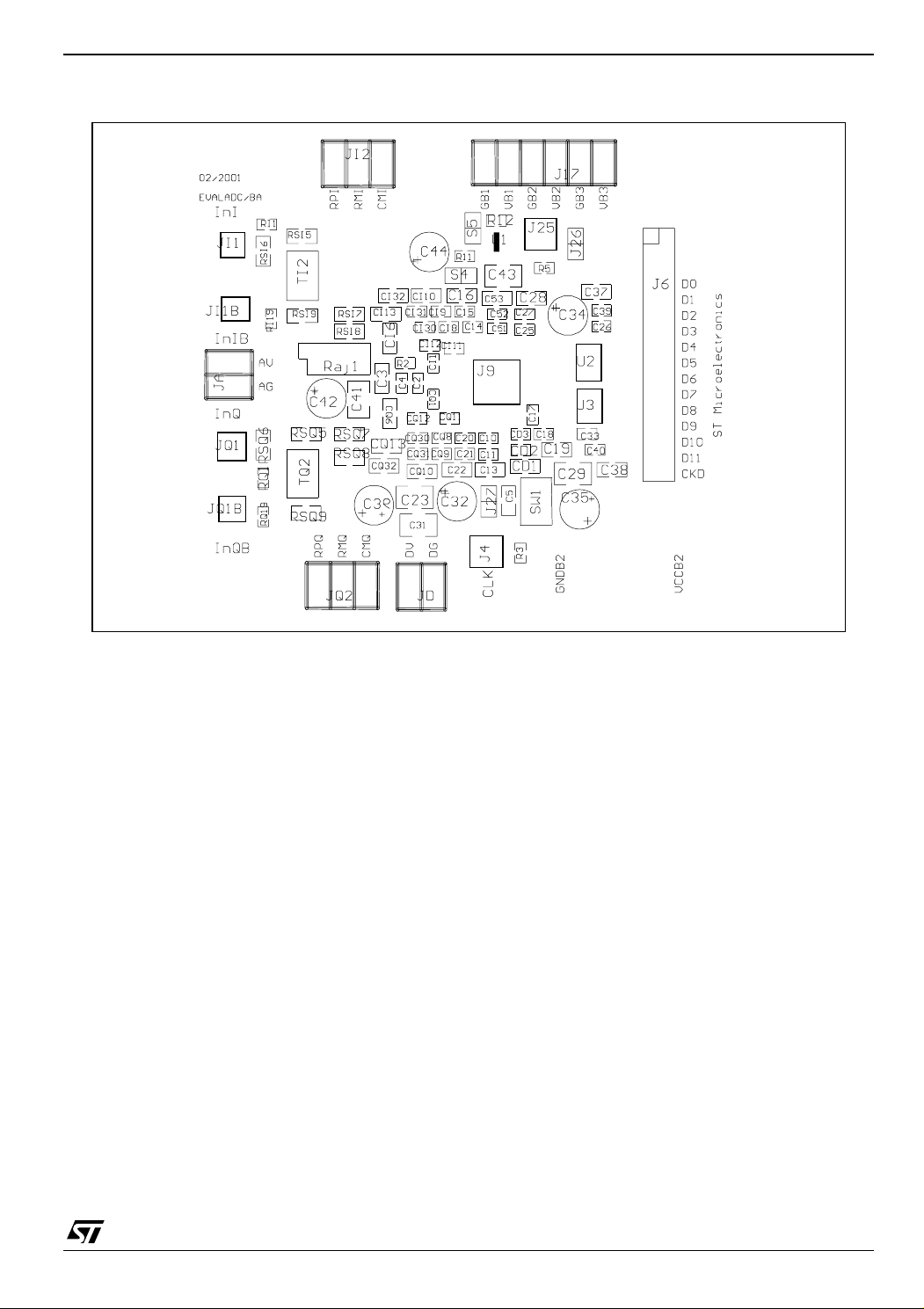
Figure 10 : Printed circuit of evaluation board.
TSA1204
17/20
Page 18
TSA1204
1
1
2
2
3
3
M
G
V
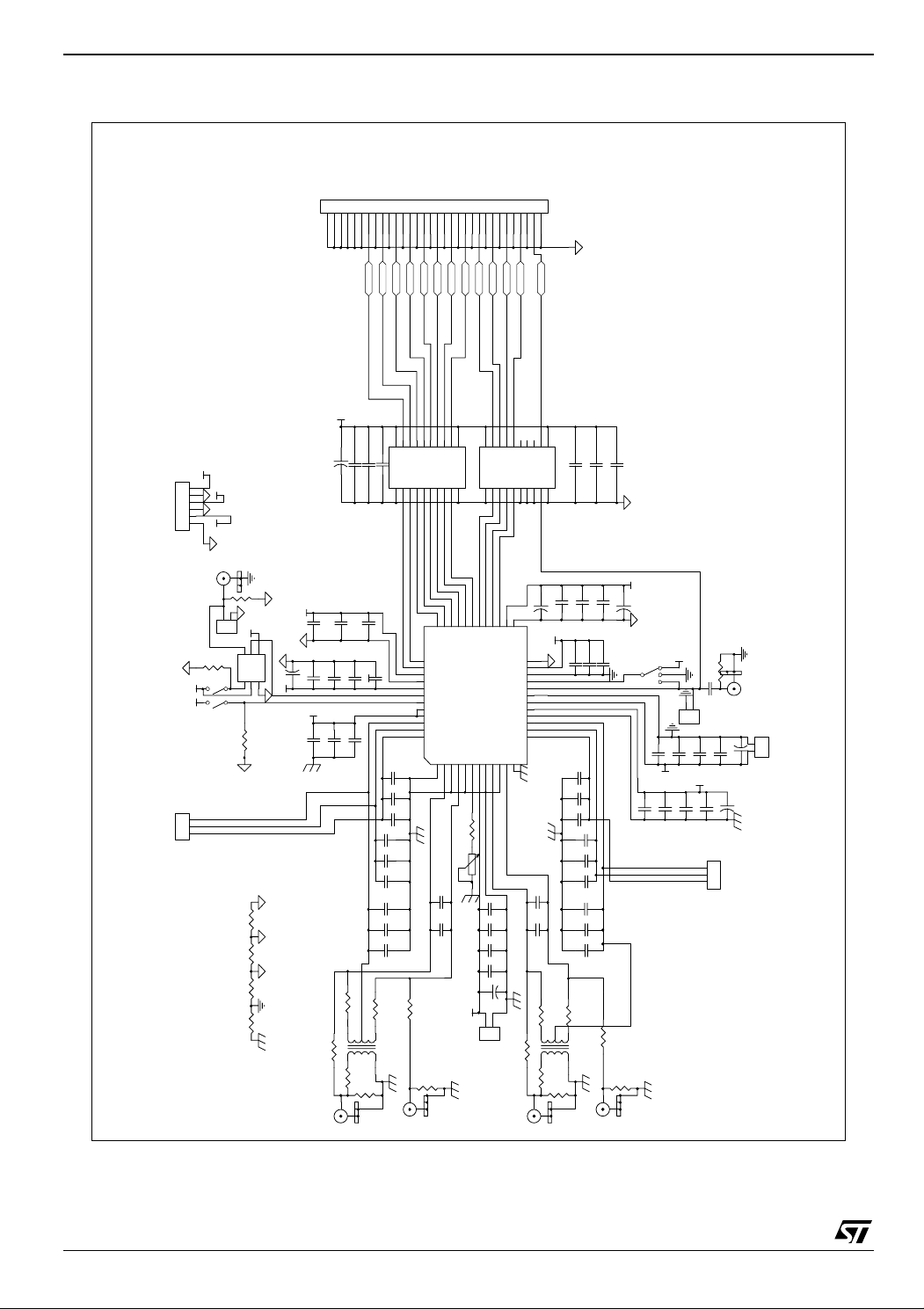
Figure 11 : TSA1204 Evaluation board schematic
D0 GND
D1 GND
D2 GND
D3 GND
D4 GND
D5 GND
D6 GND
D7 GND
D8 GND
D9 GND
D10 GND
D11 GND
CLK GND
J6
123456789
RS5 RS6 RS 7 RS 8 RS9
C C C
C C
C C
single input
differential input
Open Normal mode
Short High Impedance output mode
Switch S5
Open Normal mode
Short Test mode
VCCB3
VccB
GndB
VccB
VCCB2 Switch S4 OEB Mode
GndB
VccB
GndB
VCCB1
J17
BUFPOW
J25
CKDATA
R5
50
1
2
J26
CON2
VCCB2
S2
R12
47K
IN
U1
S5
SW-SPST
VCCB2
VCCB1
S4
SW-SPST
R11
INCM
REF
REFP
JI2
VREF I
R24
R23
R22
NM: non soudé analog input with transformer (default)
R21
VCCB2
C27
C28
470nF
D
47µF
Vcc
GNDS1
STG719
47K
0NM
0NM
0NM
0NM
C53 470nF
C43 10µF+C44
VCCB1
AVCC
C15 10nF
C16 470nF
RSI5
1011121314151617181920212223242526272829303132
D1D2D3D4D5
DO
VCCB3
20
47µF
+
C34
RSI7
0 NC
TI2
1
RSI6
C37 470nF
10nF
C52 10nF
C14 330pF
C39 10nF
C25
0
0
RI1
50
VCC
C26 330pF
OEB1D02D13D24D35D46D57D68D79GND
330pF
C51 330pF
CI11
330pF
CI12
10nF
CI13
470nF
CI30
330pF
CI31
10nF
CI32
470nF
CI8
330pF
CI9
10nF
CI10
470nF
RSI80RSI9
4326
T2-AT1-1WT
JI1B
InIB
Q019Q118Q217Q316Q415Q514Q613Q7
37
38
39
40
41
42
43
44
45
46
47
48
0 NC
RI19
50
D7D8D9
D6
12
11
20
LE
Q019Q118Q217Q316Q415Q514Q613Q7
VCC
U2
36
D1
D0(LSB)
VCCBE
GNDBE
VCCBI
VCCBI
OEB
AVCC
AVCC
INCMI
REFMI
REFPI
AGND1INI2AGND3INBI4AGND5IPOL6AVCC7AGND8INQ9AGND10INBQ11AGND
CI6
NM
CI1
33pF
74LCX573
OEB1D02D13D24D35D46D57D68D79GND
10
D929D830D731D632D533D434D335D2
8-14bits ADCJ9ADC D UAL 12B
R2
1K
Raj1
C2
C4
C3
C41
AVCC
JA
VCC
U3
27
28
26
D10
D11(MSB)
47K
330pF
10nF
470nF
10µF
C42
47µF
+
ANALOG IC
GND
D10
D11
CLK
12
11
LE
C33 330pF
C40 10nF
C38 470nF
74LCX573
10
CD2 10nF
330pF
10nF
470nF
JQ1B
330pF
10nF
470nF
330pF
10nF
470nF
InQB
VCCB2
47µF
+
C19 470nF
C35
DVCC
SW1
CD3 330pF
C10 330pF
C20 330pF
C21 10nF
RSQ9
0 NC
RQ19
50
R3
50
C5
J4
CLK
100nF
1
2
J27
CON2
C11 10nF
C13 470nF
AVCC
DVCC
C22 470nF
C23 10µF+C36
JQ2
C31 10µF+C32
47µF
INCM
REFM
REFP
VREF Q
JD
DIGITAL
ND
CC
47µF
10µF
+
C17 330pF
C29
24
23
22
21
20
19
18
17
16
15
14
13
CQ6
CQ1
RSQ70RSQ8
0 NC
TQ2
1
RSQ6
C18 10nF
DVcc
CD1 470nF
CQ11
CQ12
CQ13
CQ30
CQ31
CQ32
NM
CQ8
33pF
CQ9
CQ10
0
4326
T2-AT1-1WT
0
RQ1
50
25
VCCBE
GNDBE
GNDBI
DVCC
DGND
SELECT
CLK
DGND
DVCC
AVCC
AGND
INCMQ
REFMQ
REFPQ
12
RSQ5
18/20
Page 19
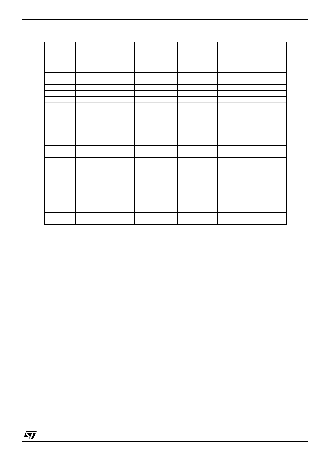
Figure 12 : Printed circuit board - List of components
Name Footprint Name Footprint Name Footprint Name Part Footprint
Part
Type
0
RSQ6
RSQ7
RSQ8
RSI6 0 805 CQ12 10nF 603 C25 330pF 603 U3 74LCX573 TSSOP20
RSI7 0 805 CQ9 10nF 603 CI1 33pF 603 U1 STG719 SOT23-6
RSI8
R3
R5
RQ19
RI1
RQ1
RI19 47 603 C11 10nF 603 C32 47µF RB.1 JD DIGITAL connector
RSI9 0NC 805 CI9 10nF 603 C37 470nF 805 JI1 InI SMA
RSQ5
RSQ9
RSI5
R24
R23
R21 0NC 805 C51 330pF 603 CI32 470nF 805 S4 SW-SPST connector
R22 0NC 805 C2 330pF 603 C13 470nF 805 TI2 T2-AT1-1WT ADT
R2
R12
R11
Raj1
C23
C41 10µF 1210 C14 330pF 603 CD1 470nF 805 NC: non soldered
C29 10µF 1210 CI30 330pF 603 C1 9 470nF 805
805 CD2 10nF 603 C26 330pF 603 CQ6 NC 805
0
805 C40 10nF 603 C20 330pF 603 CI6 NC 805
0
805 C39 10nF 603 C33 330pF 603 U2 74LCX573 TSSOP20
0
805 C52 10nF 603 CQ1 33pF 603 JA ANALOGIC connector
47
603 C18 10nF 603 C34 47µF RB.1 J17 BUFPOW connector
47
603 C21 10nF 603 C42 47µF RB.1 J25 CKDATA SMA
47
603 C4 10nF 603 C35 47µF RB.1 J4 CLK SMA
47
603 C15 10nF 603 C44 47µF RB.1 J27 CON2 SIP2
47
603 C27 10nF 603 C36 47µF RB.1 J26 CON2 SIP2
0NC
805 CI12 10nF 603 CQ10 470nF 805 JI1B InIB SMA
0NC
805 CI31 10nF 603 C28 470nF 805 JQ1 InQ SMA
0NC
805 CQ31 10nF 603 CI10 470nF 805 JQ1B InQB SMA
0NC
805 CQ30 330pF 603 CQ32 470nF 805 SW1 SWITCH connector
0NC
805 CI11 330pF 603 CQ13 470nF 805 S5 SW-SPST connector
1K
603 C17 330pF 603 C53 470nF 805 TQ2 T2-AT1-1WT ADT
47K
603 CD3 330pF 603 C16 470nF 805 JI2 VREFI connector
47K
603 C10 330pF 603 C3 470nF 805 JQ2 VREFQ connector
200K
VR5
trimmer
10µF
1210 CI8 330pF 603 C38 470nF 805
Part
Type
CQ8 330pF 603 C22 470nF 805 J6 32Pin
CQ11 330pF 603 CI13 470nF 805
Part
Type
TSA1204
Type
IDC-32
connector
19/20
Page 20

TSA1204
PACKAGE MECHANICAL DATA
48 PINS - PLASTIC PACKAGE
48 37
1
e
36
E3
E1
A
A2
A1
0,10 mm
.004 inch
SEATING PLANE
B
E
12
13 24
D3
25
c
D1
D
L1
L
0,25 mm
.010 inch
K
Millimeters Inches
Dim.
Min. Typ. Max. Min. Typ. Max.
A 1.60 0.063
A1 0.05 0.15 0.002 0.006
A2 1.35 1.40 1.45 0.053 0.055 0.057
B 0.17 0.22 0.27 0.007 0.009 0.011
C 0.09 0.20 0.004 0.008
D 9.00 0.354
D1 7.00 0.276
D3 5.50 0.216
e 0.50 0.0197
E 9.00 0.354
E1 7.00 0.276
E3 5.50 0.216
L 0.45 0.60 0.75 0.018 0.024 0.030
L1 1.00 0.039
K 0° (min.), 7° (max.)
Information furnished is bel ieved to be accurate and reliable. However, STMicroe lectronics assumes no responsibility for the
consequences of use of such information nor for any infringement of patents or other rights of third parties which may result from
its use. No li cense is granted by implication or otherwise unde r any patent or patent rights of STMicroelectronics. Specifications
mentioned in this publication ar e subject to change without notice. This publication supersedes and replaces all information
previously supplied. S TMicroelectronics products are not authorized for use as critica l components in life suppo rt devices or
systems without express written approval of STMicroelectronics.
The ST logo is a registered trademark of STMicroelectronics
GAGE PLANE
20/20
© 2003 STM icroelectronics - Pr inted in Ital y - All Rights Reserved
STMicr o el ectronics GROUP OF COMPANIES
Australi a - Brazil - Canada - Chin a - F i nl and - France - Germany - Hong Kong - Ind i a - Is rael - Ital y - J apan - Malaysia
Malta - Mor occo - Singapore - Spain - Sweden - Swi t zerland - U ni ted Kingdom - United Sta tes
http://www.st.com
 Loading...